2BWDK-DRR01Dr.AI Ring
INTOWELL BIOMEDICAL TECHNOLOGY, INC.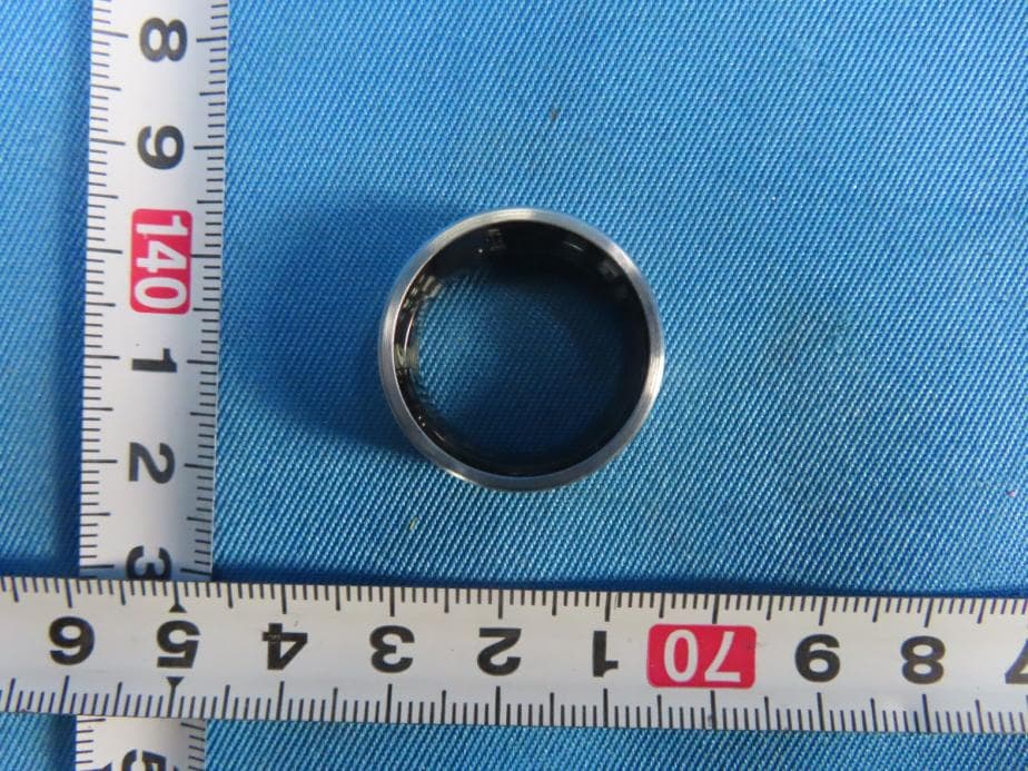
Click to zoom
Application Details
- Equipment Class
- DTS - Digital Transmission System
- Date of Grant
- Aug 11, 2026
- Application Purpose
- Original Equipment
- Equipment Note
- Dr.AI Ring
- Frequency Range
- 2402.00000000 - 2480.00000000
- Country
- Taiwan
Documents & Files
Document Text
Text extracted from the exhibit documents filed with the FCC. Open a document above to read the original.
Users Manual
Dr.AIRingUserGuide ThankyouforchoosingDr.AIRing. Toensurethebestpossibleexperience,pleasereadthisguidecarefully beforeusingthering,thecompanionapp,oranyotherDr.AI-related services.Failuretofollowtheinstructionsinthisguidemayresultin productdamage,malfunction,orpersonalinjury. 1.PackageContents Yourpackageincludesatleastthefollowingitems: Dr.AIRing×1 Dr.AIRingChargingCase×1 USBChargingCable×1 ※Ifyoudiscoveranymissingcomponents,defects,orabnormalities, pleasecontactuswithintwoweeksofpurchase. 2.ProductSpecifications ProductName:Dr.AIRing Model:DRR01 Finishes:RoseTwilight/GlacialSnowlight RingDimensions:Width7.9mm;Thickness2.8mm RingWeight:Approx.4–6g RingSizes(U.S.Standard):Sizes6–14 ExteriorMaterial:Titaniumsteel InteriorMaterial:Hypoallergenic,non-metalseamlesslining On-DeviceDataStorage:Approx.1week Battery:Rechargeablelithiumbattery(notuser-replaceable) BatteryLife:Approx.5–7days(variesbyringsize,sleeppatterns,and activitylevel) ChargingMethod:Dr.AIRingchargingcaseonly ChargingTime:Approx.30–120minutes Connectivity:BluetoothLowEnergy(BLE) FirmwareUpdates:AutomaticviatheDr.AIRingapp AppAvailability:iPhoneAppStoreandmajorAndroidappstores Privacy&Security:Encrypteddatatransmissionwithsecurepairing betweenringandapp WaterResistance:Upto50m/164ft DropResistance:Withstandsdropsfrom1m/3.3ftorequivalent impact OperatingTemperature:−10°Cto49°C(14°Fto120.2°F) ChargingTemperature:0°Cto45°C(32°Fto113°F);room temperaturerecommended ChargingCaseInput:USBType-C;usea5V/≥1Apoweradapter PowerAdapter:UseBSMI-certifiedadapterscompliantwithCNS 15598-1andrelatedstandards 3.ChargingtheRing 1.ConnecttheChargingCase InsertthesuppliedUSBType-Ccableintothechargingcase, thenconnecttheUSBType-Aendtoacompliantpowersource. 2.PlacetheRingCorrectly Aligntheringwiththeindicatorsinsidethechargingcase. Ensuretheraisedsensorinsidetheringalignswiththecenter chargingcontact. Brieflypressthebuttononthebackofthechargingcaseto activatecharging. 3.ChargingIndicatorLights Pressthebuttonforapproximatelyonesecond: Flashinggreen:Charginginprogress Solidgreen:Fullycharged Flashingred:Charging,butchargingcasebatteryislow ImportantNotes Theringdoesnotbeginchargingautomatically—youmustpress thechargingcasebutton. Chargeonlybetween0°Cand45°C(roomtemperature recommended). Usecertifiedpoweradaptersonly. Avoidcharginginexcessivelyhotorcoldenvironments. Afterfirmwareupdates,batteryreadingsmaybetemporarily inaccurate—fullyrechargetorecalibrate. 4.CheckingChargingCaseBatteryLevel Pressandholdthebuttonforapproximatelytwoseconds: Red:Below30% Orange:30%–70% Green:70%–100% 5.BatteryCalibration&ChargingTime Tocalibratethebattery: Placetheringinthechargingcaseandpressthebuttontostart charging. Continuecharginguntil100%isdisplayedandforatleast60 minutestotal. Afullydepletedringrequiresapproximately120minutesto recharge. Notes Withoutexternalpower,thechargingcasewillchargetheringto approximately95%topreservebatterylongevity. Toreach100%,connectthechargingcasetoanexternalpower sourceduringcharging. 4.InstallingtheDr.AIRingApp 1.Search“Dr.AIRing”intheAppStoreorAndroidappstore andinstalltheapp. 2.Opentheapp,registeranewaccount,confirmyour activationemail,login,andcompleteyourbasicprofile. 5.PairingtheRing 1.Placetheringinthechargingcaseandpressthebuttonto wakeit. 2.EnsureBluetoothisenabledonyoursmartphone. 3.OpentheDr.AIRingappandselectthedevicematchingyour ringsizeandmodeltocompletepairing. 4.ReplacingYourRing:Toswitchtoadifferentring,goto "More"→"Device"andselect"SetUpaNewRing."Thenewring willoverwritethesettingsofthecurrentone. 5.TransferringOwnership:Ifyouaregivingtheringtosomeone else,werecommendgoingto"More"→"Device"andselecting "FactoryReset."Thisensuresallinternaldataandpersonal settingsarecleared. 6.Long-termStorage:Ifyoudonotplantousetheringfora longtime,fullychargeitfirst,thengoto"More"→"Device"and select"PowerOff"tosavebattery.Toreactivatethering,simply placeitonthechargingdock;itwillturnbackononceitstarts charging. 6.WearingtheRing Rotatetheringsotheraisedinnersensorrestsagainstthefingerpad. Properalignmentimprovesmeasurementaccuracy. 7.Support&Assistance Forquestionsaboutsetup,usage,orserviceissues,pleasevisit: Officialwebsite:https://www.draiai.com Oremail:[email protected] 8.SafetyInformation Dr.AIservicesarenotintendedforthediagnosis,treatment,cure,or preventionofanydiseaseormedicalcondition.Allinformationand recommendationsprovidedbyDr.AIareforgeneralreference purposesonlyanddonotreplaceevaluation,judgment,ortreatment byqualifiedmedicalprofessionals. Ifyouhaveanyquestionsregardingthehealthinformationprovided byDr.AI,oranyadjustmentrecommendationsbasedonyoursleepor activitydata,youmustconsultaqualifiedhealthcareprofessional.Do notdelay,disregard,orsubstituteprofessionalmedicalcarebasedon anycontentprovidedbyDr.AI. Dr.AIshallbearnoresponsibilityorliabilitywhatsoeverforanyhealth issuesthatmayariseasaresultofusinginformationor recommendationsprovidedthroughDr.AI-relatedservices.Ifyou choosetomakeanyadjustmentsbasedonDr.AIsleeporactivity recommendations,youacknowledgeandagreethatyouvoluntarily assumeallrisksarisingtherefrom.. Youmustcarefullymonitoryourphysicalconditionandresponses.For example,ifchangesinsleeporactivitypatternsresultinunexpected, recurring,orpersistentpain,fatigue,oranyformofdiscomfort,you arestronglyadvisedtoconsultaphysicianbeforecontinuingor implementingfurtheradjustments. Additionally,ifduetopersonalhealthconditionsorrarephysiological differencesyourbodilyfunctionsorresponsesdiffersignificantlyfrom generalpopulationaverages,informationorguidanceprovidedby Dr.AIservicesmaybemisleading.Insuchcases,youmustconsulta qualifiedhealthcareprofessionalbeforereferencingoradoptingany Dr.AI-providedinformationorrecommendations. Whenliftingheavyobjectsorperformingphysicalmovement,ensure thattheringoranyotherDr.AIRingproductsarenotcaught, pinched,ortrappedbyfixedstructuresorheavyobjects,inorderto preventinjuryordamage. Ifyourfingershowsredness,itching,swelling,orothersi…
Text truncated - open the document above for the full version.
External Photos
FCCID:2BWDK-DRR01 FCCID:2BWDK-DRR01 FCCID:2BWDK-DRR01 FCCID:2BWDK-DRR01 FCCID:2BWDK-DRR01 FCCID:2BWDK-DRR01 FCCID:2BWDK-DRR01 FCCID:2BWDK-DRR01 FCCID:2BWDK-DRR01
ID Label/Location Info
LabelandLabelLocation Theproductistoosmalltobeengraved. TheFCCIDandMIClogoistypedontheusermanualandontheproductpackag. Packagphoto:
Internal Photos
FCCID:2BWDK-DRR01 FCCID:2BWDK-DRR01 FCCID:2BWDK-DRR01
RF Exposure Info
Page 1 of 2 RF EXPOSURE EVALUATION FCC ID: 2BWDK-DRR01 Product Name : Dr.AI Ring Model Name : DRR01 Bluetooth Version : BT5.2 BLE Operating frequency : 2402-2480MHz Numbers of Channel : 40 channels For DTS Antenna Type : Chip Antenna Antenna Gain : 2.28 dBi Type of Modulation : GFSK Power supply : Input:5V, 1A Li-ion Battery :170724 Voltage: 3.7V Capacity:16.5 mAh Hardware Version : SR30_V1.0 Software Version : V03.00.06 Page 2 of 2 Standard Requirement According to § 15.247(i) and § 1.1307b(1), systems operating under the provisions of this section shall be operated in a manner that ensures that the public is not exposed to radio frequency energy levels in excess of the Commission’s guidelines. See KDB 447498 D01 General RF Exposure Guidance v06, section 4. 3. 1. The 1-g and 10-g SAR test exclusion thresholds for 100MHz to 6GHz at test separation distances ≤ 50mm are determined by: [ (max. power of channel, including tune-up tolerance, mW)/(min. test separation distance, mm)]*[ √f(GHz)] ≤3.0 for 1-g SAR and ≤7.5 for 10-g SAR extremity SAR, where ⚫ f(GHz) is the RF channel transmit frequency in GHz ⚫ Power and distance are rounded to the nearest mW and mm before calculation ⚫ The result is rounded to one decimal place for comparison. The test exclusions are applicable only when the minimum test separation distance is ≤ 50mm and for transmission frequencies between 100MHz and 6GHz. When the minimum test separation distance is <5mm, a distance of 5mm is applied to determine SAR test exclusion. Routine SAR evaluation refers to that specifically required by § 2.1093, using measurements or computer simulation. When routine SAR evaluation is not required, portable transmitters with output power greater than the applicable low threshold require SAR evaluation to quality for TCB approval. Channel (MHz) Maximum output power (dBm) Tune up tolerance (dBm) Max Tune Up Power (mW) Distance (mm) Calculation results Limit Operating Mode 2480 -2.22 -2.22±1 0.755092 5 0.237824 3 BLE According to KDB 447498, no stand-alone required for BT antenna, and no simultaneous SAR measurement is required. Signature Simon Pu Manager Date: 2025-04-16
Test Report
Page 1 of 60 FCC TEST REPORT FCC ID: 2BWDK-DRR01 Product : Dr.AI Ring Model Name : DRR01 Brand : Dr.AI Report No. : PTC26012314703E-FC01 Prepared for INTOWELL BIOMEDICAL TECHNOLOGY, INC. 4 F., No. 88, Changan W. Rd., Datong Dist., Taipei City 10351 Taiwan Prepared by Precise Testing & Certification Co., Ltd Building 1, No. 6, Tongxin Road, Dongcheng Street, Dongguan, Guangdong, China Report No.: PTC26012314703E-FC01 Page 2 of 60 1 TEST RESULT CERTIFICATION Applicant’s name : INTOWELL BIOMEDICAL TECHNOLOGY, INC. Address : 4 F., No. 88, Changan W. Rd., Datong Dist., Taipei City 10351 Taiwan Manufacture's name : INTOWELL BIOMEDICAL TECHNOLOGY, INC. Address : 4 F., No. 88, Changan W. Rd., Datong Dist., Taipei City 10351 Taiwan Product name : Dr.AI Ring Model name : DRR01 Standards : FCC CFR47 Part 15 Section 15.247 Test procedure : ANSI C63.10-2020 Test Date : Mar. 18, 2026 to Apr. 17, 2026 Date of Issue : Apr. 17, 2026 Test Result : Pass This device described above has been tested by PTC, and the test results show that the equipment under test (EUT) is in compliance with the FCC requirements. And it is applicable only to the tested sample identified in the report. This report shall not be reproduced except in full, without the written approval of PTC, this document may be altered or revised by PTC, personal only, and shall be noted in the revision of the document. Test Engineer: Jack zhou / Engineer Technical Manager: Simon Pu / Manager Report No.: PTC26012314703E-FC01 Page 3 of 60 Contents Page 1 TEST RESULT CERTIFICATION .............................................................................................................................. 2 2 TEST SUMMARY ......................................................................................................................................................... 5 2.1 TEST SITE ........................................................................................................................................................... 6 3 GENERAL INFORMATION ..................................................................................................................................... 7 3.1 GENERAL DESCRIPTION OF E.U.T. .................................................................................................................... 7 3.2 CHANNEL LIST .................................................................................................................................................... 8 4 EQUIPMENT DURING TEST .................................................................................................................................. 9 4.1 EQUIPMENTS LIST ............................................................................................................................................ 9 4.2 MEASUREMENT UNCERTAINTY ......................................................................................................................... 11 4.3 DESCRIPTION OF SUPPORT UNITS ................................................................................................................... 12 5 CONDUCTED EMISSION ......................................................................................................................................... 13 5.1 E.U.T. OPERATION ........................................................................................................................................... 13 5.2 EUT SETUP ...................................................................................................................................................... 13 5.3 TEST SET-UP (BLOCK DIAGRAM OF CONFIGURATION) .................................................................................. 14 5.4 MEASUREMENT PROCEDURE ........................................................................................................................... 14 5.5 CONDUCTED EMISSION LIMIT ........................................................................................................................... 14 5.6 MEASUREMENT DESCRIPTION .......................................................................................................................... 14 5.7 CONDUCTED EMISSION TEST RESULT ............................................................................................................. 14 6 RADIATED SPURIOUS EMISSIONS ..................................................................................................................... 17 6.1 EUT OPERATION .............................................................................................................................................. 17 6.2 TEST SETUP ..................................................................................................................................................... 18 6.3 SPECTRUM ANALYZER SETUP .......................................................................................................................... 19 6.4 TEST PROCEDURE ............................................................................................................................................ 20 6.5 SUMMARY OF TEST RESULTS .......................................................................................................................... 22 7 CONDUCT BAND EDGE AND SPURIOUS EMISSIONS MEASUREMENT ................................................... 30 7.1 TEST PROCEDURE ............................................................................................................................................ 30 7.2 TEST SETUP ..................................................................................................................................................... 30 7.3 TEST RESULT ................................................................................................................................................... 31 Report No.: PTC26012314703E-FC01 Page 4 of 60 8 6DB BANDWIDTH MEASUREMENT ..…
Text truncated - open the document above for the full version.
Test Report
承 認 書 SPECIFICATION FOR APPROVAL 客戶名稱 CUSTOMER : 客戶料號 CUSTOMER’S P/N : 料號 PART NUMBER : WAN1608H245H08 規格 DESCRIPTION : Chip Antenna 1608 MH-Ant 2.45G Type H08 版本 VERSION : V1.0 日期 ISSUE DATE : 2021/03/03 客 戶 承 認 CUSTOMER APPROVED 工 程 部 R&D CENTER 承 認 APPROVAL 確 認 CHECKED 製 作 DRAWN Ray Tennyson Snow 萬誠科技股份有限公司 OneWave Electronic Co., Ltd. 112台北市北投區立功街151號1樓 1F, No. 151, Li Gong Street, Beitou District, Taipei City 112, Taiwan 電話: (02) 2898-2220 TEL: +886 2 2898-2220 傳真: (02) 2898-5055 FAX: +886 2 2898-5055 ONEWAVE TECHNOLOGY CO., LTD. 2/12 1608 Chip antenna For Bluetooth / WLAN Applications Dimension (mm) L 1.70 ± 0.20 W 0.93 ± 0.20 T 0.75 ± 0.20 P/N: WAN1608H245H08 ONEWAVE TECHNOLOGY CO., LTD. 3/12 Part Number Information WAN 1608 H 245 H 08 A B C D E F A Product Series Antenna B Dimension L x W 1.6X0.8mm (+-0.2mm) C Material High K material D Working Frequency 2.4 ~ 2.5GHz E Feeding mode Monopole & Single Feeding F Antenna type Type = 08 1. Electrical Specification Remark : Bandwidth & Peak Gain was measured under evaluation board of next page Specification Part Number WAN1608H245H08 Central Frequency 2450 MHz Bandwidth 120 (Min.) MHz Return Loss -10(Max) dB Peak Gain 2.28 dBi Impedance 50 Ohm Operating Temperature -40~+110 °C Maximum Power 4 W Resistance to Soldering Heats 10 ( @ 260°C) sec. Polarization Linear Azimuth Beamwidth Omni-directional Termination Cu / Sn (Leadless) ONEWAVE TECHNOLOGY CO., LTD. 4/12 2. Recommended PCB Pattern 1. Evaluation Board Dimension (若淨空區夠大,建議在天線尾段加Trace,效能更佳) Unit : mm 2. Evaluation Board Dimension (若淨空區夠大,建議在天線尾段加Trace,效能更佳) 3. Evaluation Board Dimension ONEWAVE TECHNOLOGY CO., LTD. 5/12 Suggested Matching Circuit 重要資訊 : 匹配元件建議使用精準度高的電感±0.1~0.3nH、電容±0.1pF 1. Layout Dimensions in Clearance area(Size=5.5*4mm) 50 ohm transmission Line Matching Circuit 2. Layout Dimensions in Clearance area(Size=5.5*4mm) 50 ohm transmission Line Matching Circuit 1~10nH None 0Ω 1.5pF ONEWAVE TECHNOLOGY CO., LTD. 6/12 3. Layout Dimensions in Clearance area(Size=5*3mm) 50 ohm transmission Line Matching Circuit FootPrint (Unit : mm) ONEWAVE TECHNOLOGY CO., LTD. 7/12 3. Measurement Results Return Loss ONEWAVE TECHNOLOGY CO., LTD. 8/12 Radiation Pattern Efficiency Peak Gain Directivity 2400MHz 50.65 % 1.80 dBi 3.95 dBi 2450MHz 53.27 % 2.28 dBi 4.42 dBi 2500MHz 50.32 % 1.77 dBi 4.15 dBi Chamber Coordinate System Y Z X ONEWAVE TECHNOLOGY CO., LTD. 9/12 4.Reliability and Test Condictions ITEM REQUIREMENTS TEST CONDITION Solderability 1. Wetting shall exceed 90% coverage 2. No visible mechanical damage Pre-heating temperature:150°C/60sec. Solder temperature:230±5°C Duration:4±1sec. Solder:Sn-Ag3.0-Cu0.5 Flux for lead free: rosin Solder heat Resistance 1. No visible mechanical damage 2. Central Freq. change :within ± 6% 10 ± 0.5 sec. 60 sec . . T E M P ( °C ) 150 °C 2 6 0 °C Pre-heating temperature:150°C/60sec. Solder temperature:260±5°C Duration:10±0.5sec. Solder:Sn-Ag3.0-Cu0.5 Flux for lead free: rosin Component Adhesion (Push test) 1. No visible mechanical damage The device should be reflow soldered(230±5°C for 10sec.) to a tinned copper substrate A dynometer force gauge should be applied the side of the component. The device must with-ST-F 0.5 Kg without failure of the termination attached to component. Component Adhesion (Pull test) 1. No visible mechanical damage Insert 10cm wire into the remaining open eye bend ,the ends of even wire lengths upward and wind together. Terminal shall not be remarkably damaged. Thermal shock 1. No visible mechanical damage 2. Central Freq. change :within ±6% Phase Temperature(°C) Time(min) 1 +110±5°C 30±3 2 Room Temperature Within 3sec 3 -40±2°C 30±3 4 Room Temperature Within 3sec +110°C=>30±3min -40°C=>30±3min Test cycle:10 cycles The chip shall be stabilized at normal condition for 2~3 hours before measuring. Resistance to High Temperature 1. No visible mechanical damage 2. Central Freq. change :within ±6% 3. No disconnection or short circuit. Temperature: +110±5°C Duration: 1000±12hrs The chip shall be stabilized at normal condition for 2~3 hours before measuring. Resistance to Low Temperature 1. No visible mechanical damage 2. Central Freq. change :within ±6% 3. No disconnection or short circuit. Temperature:-40±5°C Duration: 1000±12hrs The chip shall be stabilized at normal condition for 2~3 hours before measuring. Humidity 1. No visible mechanical damage 2. Central Freq. change :within ±6% 3. No disconnection or short circuit. Temperature: 40±2°C Humidity: 90% to 95% RH Duration: 1000±12hrs The chip shall be stabilized at normal condition for 2~3 hours before measuring. 4±1 sec. 60sec TEMP (°C) 150°C 230°C ONEWAVE TECHNOLOGY CO., LTD. 10/12 5.Soldering and Mounting Mildly activated rosin fluxes are preferred. The minimum amount of solder can lead to damage from the stresses caused by the difference in coefficients of expansion between solder, chip and substrate. The terminations are suitable for all wave and re-flow soldering systems. If hand soldering cannot be avoided, the preferred technique is the utilization of hot air soldering tools. Recommended temperature profiles for re-flow soldering in Figure 1. Products attachment with a soldering iron is discouraged due to the inherent process control limitations. In the event that a soldering iron must be employed the following precautions are recommended. ‧Preheat circuit and products to 150°C ‧Never contact the ceramic with the iron tip ‧Use a 20 watt soldering iron with tip diameter of 1.0mm ‧280°C tip temperature (max) ‧1.0mm tip diameter (max) ‧Limit soldering time to 3 sec. SOLDERING COOLING NATURAL PRE-HEATING TEMPERATURE(°C) 60~120 s 10s max. 30~60s 250~260 230 180 150 TIME(sec.) Reflow Soldering SOLDERING COOLING NATURAL PRE-HEATING TEMPERATURE(°C) within 3s Gradual cooling 150 TIME(sec.) Iron Soldering Over 60s 350 300 ONEWAVE TECHNOLOGY CO., LTD. 11/12 6.Packaging Information ◆ Tape Specification: W Ao Bo Ko P F E D D1 Po P2 t 8.0 ±0.30 1.10± 0.05 1.90 ±0.10 1.10± 0.10 4.00 ±0.05…
Text truncated - open the document above for the full version.
Test Setup Photos
FCCID:2BWDK-DRR01 ConductedEmissions RadiatedSpuriousEmissions From30MHz-1000MHz FCCID:2BWDK-DRR01 TestfrequencyfromAbove1GHz
Contact Information
Applicant
sean ku(CTO)
[email protected]Fax: +886 0225582326-155
Technical Contact
Genix Networks Inc.Yi Cheng Hsieh
Suite 800, 251 S. Lake Ave. Pasadena, CA 91101 · Pasadena, California · United States
Test Firm
Precise Testing & Certification Co., LTD.Yang Juan
Technical Specifications
| # | Rule Parts | Frequency Range | Power Output |
|---|---|---|---|
| 1 | 15C | 2.40 GHz - 2.48 GHz | 600.00 µW |