2BWHV-LUNETTEV2Lunette
Calm and Sense Technologies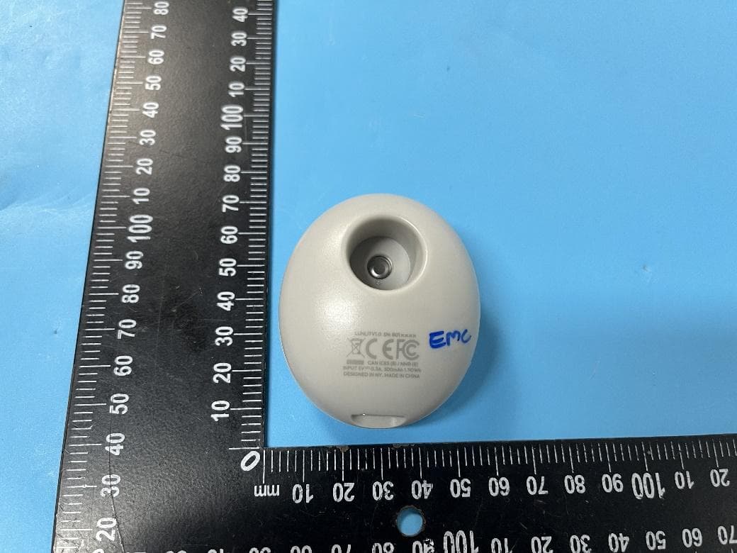
Click to zoom
Application Details
- Equipment Class
- DTS - Digital Transmission System
- Date of Grant
- Aug 20, 2026
- Application Purpose
- Original Equipment
- Equipment Note
- Lunette
- Frequency Range
- 2402.00000000 - 2480.00000000
- Company
- Calm and Sense Technologies
- Country
- United States
Documents & Files
Document Text
Text extracted from the exhibit documents filed with the FCC. Open a document above to read the original.
Users Manual
QUICK START GUIDE WHAT’S IN THE BOX everything you need. lunette scent capsules charging cable LIGHTS & STATUS SUNSET • breathing BLUE • breathing AMBER • breathing RED • blinking GREEN • solid session in progress ready to connect fully charged charging battery low your lunette talks in color. GETTING STARTED three simple steps. remove the cap. pop the capsule into the bottom of your Lunette. PUT IT WHERE YOU FEEL IT. rest it on your chest or hold it in your palm. whatever feels best. PRESS ONCE. BREATHE. inhale as the light and vibration rise. exhale as they fade. POP IN A CAPSULE CONNECT TO THE APP make lunette yours. scan below to personalize your experience, update your device, and discover new scents. the app is optional. your lunette works on its own. CARE & MAINTENANCE keep your lunette at its best. charge with the included USB-C cable. CHARGING wipe with a soft, slightly damp cloth. never immerse in water. CLEANING store in a cool, dry place away from direct sunlight. STORAGE recap capsules between uses to keep the scent fresh. CAPSULES SAFETY & TROUBLESHOOTING just in case. designed and tested for use with your lunette device. USE ONLY LUNETTE CAPSULES small parts may present a choking hazard. KEEP AWAY FROM KIDS & PETS do not ingest capsule contents. FOR EXTERNAL USE ONLY do not use if the housing, USB-C port, or capsule is damaged. STOP USE IF DAMAGED charge for 15 minutes. if there is no light, hold the button for 10 seconds. WON’T TURN ON? make sure capsule is fully seated & contains fragrance. NO MIST? visit getlunette.com/support NEED MORE HELP? open the lunette app and follow the pairing instructions. WON’T CONNECT? This device complies with part 15 of the FCC Rules. Operation is subject to the following two conditions: (1) this device may not cause harmful interference, and (2) this device must accept any interference received, including interference that may cause undesired operation. CAUTION: The grantee is not responsible for any changes or modifications not expressly approved by the party responsible for compliance. Such modifications could void the user’s authority to operate the equipment. NOTE: This equipment has been tested and found to comply with the limits for a Class B digital device, pursuant to part 15 of the FCC Rules. These limits are designed to provide reasonable protection against harmful interference in a residential installation. This equipment generates, uses, and can radiate radio frequency energy, and if not installed and used in accordance with the instructions, may cause harmful interference to radio communications. However, there is no guarantee that interference will not occur in a particular installation. If this equipment does cause harmful interference to radio or television reception, which can be determined by turning the equipment off and on, the user is encouraged to try to correct the interference by one or more of the following measures: – Reorient or relocate the receiving antenna. – Increase the separation between the equipment and receiver. – Connect the equipment into an outlet on a circuit different from that to which the receiver is connected. – Consult the dealer or an experienced radio/TV technician for help. FCC COMPLIANCE STATEMENT This device contains license-exempt transmitter(s)/receiver(s) that comply with Innovation, Science and Economic Development Canada license-exempt RSS(s). Operation is subject to the following two conditions: (1) This device may not cause interference. (2) This device must accept any interference, including interference that may cause undesired operation of the device. L’émetteur/récepteur exempt de licence contenu dans le présent appareil est conforme aux CNR d’Innovation, Sciences et Développement économique Canada applicables aux appareils radio exempts de licence. L’exploitation est autorisée aux deux conditions suivantes : 1) L’appareil ne doit pas produire de brouillage; 2) L’appareil doit accepter tout brouillage radioélectrique subi, même si le brouillage est susceptible d’en compromettre le fonctionnement. CANADIAN COMPLIANCE STATEMENT PRODUCT NAME: PRODUCT MODEL: FCC ID: IC: LUNETTE LUNETTE-V2 2BWHV-LUNETTEV2 35778-LUNETTEV2 CALM AND SENSE TECHNOLOGIES, INC. scan the code or visit getlunette.com email [email protected] follow @getlunette ANY QUESTIONS? New York, NY 10036 DESIGNED IN NY, MADE IN CHINA
Attestation Statements
Calm and Sense Technologies 106 Playa Rienta Way Palm Beach Gardens, FL 33418 Date: 07/14/26 Federal Communications Commission Authorization and Evaluation Division 7435 Oakland Mills Road Columbia, MD 21046 FCC ID: 2BWHV-LUNETTEV2 Attestation Statements Part 2.911(d)(5)(i) Filing To whom it may concern, Calm and Sense Technologies, certifies that the equipment for which authorization is sought is not “covered” equipment prohibited from receiving an equipment authorization pursuant to the section 2.903 of the FCC rules. Calm and Sense Technologies certifies that the equipment for which authorization is sought does not include cybersecurity or anti-virus software produced or provided by Kaspersky Lab, Inc. or any of its successors and assignees, including equipment with integrated Kaspersky Lab, Inc. (or any of its successors and assignees) cybersecurity or anti-virus software pursuant to DA-24-886 and KDB 986446 D01 Covered Equipment Guidance section B(2a). Device is inherently compliant based on hardware limitations or software controls. or A Software Bill of Materials (SBOM) is provided to the TCB for review, and The end-user or third parties cannot install additional software on this device. Sincerely, Signature: Daniel Shuter Founder
Attestation Statements
Calm and Sense Technologies 106 Playa Rienta Way Palm Beach Gardens, FL 33418 Date: 07/14/26 Federal Communications Commission Authorization and Evaluation Division 7435 Oakland Mills Road Columbia, MD 21046 FCC ID: 2BWHV-LUNETTEV2 Attestation Statements Part 2.911(d)(5)(ii) Filing To whom it may concern, Calm and Sense Technologies certifies that, as of the date of the filing of the application, Calm and Sense Technologies is not identified on the Covered List (as a specifically named entity or any of its subsidiaries or affiliates) as an entity producing “covered” equipment. Sincerely, Signature: Daniel Shuter Founder
Attestation Statements
Calm and Sense Technologies 106 Playa Rienta Way Palm Beach Gardens, FL 33418 Date: 07/14/26 Federal Communications Commission Authorization and Evaluation Division 7435 Oakland Mills Road Columbia, MD 21046 FCC ID: 2BWHV-LUNETTEV2 FRN: 0038507091 US Agent – Attestation Statement / Part 2.911(d)(7) To whom it may concern, Calm and Sense Technologies (“the applicant”) certifies that, as of the date of the filing of the application, Calm and Sense Technologies is our designated U.S. agent for service of process for the above referenced FCC ID. Calm and Sense Technologies accepts to maintain an agent for no less than one year after the grantee has terminated all marketing and importation or the conclusion of any Commission-related proceeding involving the equipment. Calm and Sense Technologies accepts, as of the date of the filing of the application, the obligation of the designated U.S. agent for service of process for the above referenced FCC ID. Designated U.S. Agent Information: Name: Calm and Sense Technologies FRN: 0038507091 Address: 106 Playa Rienta Way, Palm Beach Gardens, FL 33418 Contact Person: Daniel Shuter Tel.: (561) 324-5485 Email: [email protected] Sincerely, Company: Calm and Sense Technologies Designated Agent: Calm and Sense Technologies Company Representative: Daniel Shuter Designated Agent Representative: Daniel Shuter Signature: Signature:
Cover Letter(s)
Calm and Sense Technologies 106 Playa Rienta Way Palm Beach Gardens, FL 33418 Date: 07/14/26 Federal Communications Commission Authorization and Evaluation Division 7435 Oakland Mills Road Columbia, MD 21046 FCC ID: 2BWHV-LUNETTEV2 Confidentiality Request To whom it may concern, Pursuant to Sections 0.457 and 0.459 of the Commission’s Rules, we hereby request confidential treatment of the information accompanying this application as outlined below: ☒Block Diagram ☐Tune-Up Information ☒Operational Description ☐Security Information ☒Schematics ☐Software Defined Radio (SDR) Information ☒Parts List The above materials contain trade secrets and proprietary information not customarily released to the public. The public disclosure of these matters might be harmful to the applicant and provide unjustified benefits to its competitors. The applicant understands that pursuant to Rule 0.457, disclosure of this application and all accompanying documentation will not be made before the date of the Grant for this application. Sincerely, Signature: Daniel Shuter Founder
Cover Letter(s)
Calm and Sense Technologies 106 Playa Rienta Way Palm Beach Gardens, FL 33418 Date: 07/14/26 Federal Communications Commission Authorization and Evaluation Division 7435 Oakland Mills Road Columbia, MD 21046 FCC ID: 2BWHV-LUNETTEV2 Declaration of Authorization To whom it may concern, I, the undersigned, hereby authorize, Jandy So, of Waltek Testing Group (Shenzhen) Co., Ltd., (WALTEK) to act on our behalf in all manners relating to application for equipment authorization, including signing of all documents relating to these matters. Any and all acts carried out by Jandy So, of Waltek Testing Group (Shenzhen) Co., Ltd., (WALTEK) on our behalf shall have the same effects as acts of our own. I, the undersigned, hereby certify that we are not subject to a denial of federal benefits, that includes FCC benefits, pursuant to Section 5301 of the Anti-Drug Abuse Act of 1988, 21 U.S.C 853(a). This authorization is valid until further written notice from the applicant. Sincerely, Signature: Daniel Shuter Founder
External Photos
ReferenceNo.:WTX26X05125506WPage2of14 WaltekTestingGroup(Shenzhen)Co.,Ltd. Http://www.waltek.com.cn EXHIBIT2-EUTEXTERNALPHOTOGRAPHS EUTView1 EUTView2 ReferenceNo.:WTX26X05125506WPage3of14 WaltekTestingGroup(Shenzhen)Co.,Ltd. Http://www.waltek.com.cn EUTView3 EUTView4 ReferenceNo.:WTX26X05125506WPage4of14 WaltekTestingGroup(Shenzhen)Co.,Ltd. Http://www.waltek.com.cn EUTView5 EUTView6 ReferenceNo.:WTX26X05125506WPage5of14 WaltekTestingGroup(Shenzhen)Co.,Ltd. Http://www.waltek.com.cn EUTView7
ID Label/Location Info
ReferenceNo.:WTX26X05125506WPage1of14 WaltekTestingGroup(Shenzhen)Co.,Ltd. Http://www.waltek.com.cn ANNEX EXHIBIT1-PRODUCTLABELING ProposedFCCIDLabelFormat ProductLabelPackagingLabel ProposedLabelLocationonEUT FCCIDLabel Location
Internal Photos
ReferenceNo.:WTX26X05125506WPage6of14 WaltekTestingGroup(Shenzhen)Co.,Ltd. Http://www.waltek.com.cn EXHIBIT3-EUTINTERNALPHOTOGRAPHS EUTHousingand BoardView1 EUTHousingand BoardView2 ReferenceNo.:WTX26X05125506WPage7of14 WaltekTestingGroup(Shenzhen)Co.,Ltd. Http://www.waltek.com.cn EUTHousingand BoardView3 Solder Board-Component View1 ReferenceNo.:WTX26X05125506WPage8of14 WaltekTestingGroup(Shenzhen)Co.,Ltd. Http://www.waltek.com.cn Solder Board-Component View2 Solder Board-Component View3 ReferenceNo.:WTX26X05125506WPage9of14 WaltekTestingGroup(Shenzhen)Co.,Ltd. Http://www.waltek.com.cn Solder Board-Component View4 Solder Board-Component View5 ReferenceNo.:WTX26X05125506WPage10of14 WaltekTestingGroup(Shenzhen)Co.,Ltd. Http://www.waltek.com.cn AntennaView LEAntenna
RF Exposure Info
WaltekTestingGroup(Shenzhen)Co.,Ltd. Http://www.waltek.com.cn RFEXPOSUREREPORT ReferenceNo.......................:WTX26X05125506W002 FCCID....................................:2BWHV-LUNETTEV2 Applicant...............................:CalmandSenseTechnologies Address.................................:106PlayaRientaWay,PalmBeachGardens,FL33418 Manufacturer........................:ThesameasApplicant Address ................................. :ThesameasApplicant ProductName......................:Lunette ModelNo... ............................ :LUNETTE-V2 Standards..............................: FCCRulePart1.1307 KDB447498D04 DateofReceiptsample ..... :2026-05-09 DateofTest...........................:2026-05-09to2026-06-04 DateofIssue ........................ :2026-06-04 ReportFormNo................... : WTX_Part1_1307W Result.....................................:Pass Remarks: Theresultsshowninthistestreportreferonlytothesample(s)tested,thistestreportcannotbe reproduced,exceptinfull,withoutpriorwrittenpermissionofthecompany.Thereportwouldbeinvalidwithout specificstampoftestinstituteandthesignaturesofapprover. PreparedBy: WaltekTestingGroup(Shenzhen)Co.,Ltd. Address:1/F.,Room101,Building1,HongweiIndustrialPark,Liuxian2ndRoad, Block70Bao'anDistrict,Shenzhen,Guangdong,China Tel.:+86-755-33663308Fax.:+86-755-33663309Email:[email protected] Testedby:Approvedby: MikeShi/ProjectEngineerJasonSu/Manager WaltekTestingGroup(Shenzhen)Co.,Ltd. Http://www.waltek.com.cn 1GeneralInformation GeneralDescriptionofEUT ProductName:Lunette TradeName/ ModelNo.:LUNETTE-V2 AddingModel(s):/ RatedVoltage: ChargingPort:DC5V Battery:DC3.7V BatteryCapacity:300mAh PowerAdapter:/ EquipmentType:Portabledevice TechnicalCharacteristicsofEUT BluetoothVersion:V5.0(LEmode) FrequencyRange:2402-2480MHz RFOutputPower:-3.35dBm(Conducted) DataRate:1Mbps Modulation:GFSK QuantityofChannels:40 ChannelSeparation:2MHz TypeofAntenna:CeramicsAntenna AntennaGain:2.12dBi 2TestFacility Addressofthetestlaboratory Laboratory:WaltekTestingGroup(Shenzhen)Co.,Ltd. Address:1/F.,Room101,Building1,HongweiIndustrialPark,Liuxian2ndRoad,Block70Bao'anDistrict, Shenzhen,Guangdong,China FCC–RegistrationNo.:125990 WaltekTestingGroup(Shenzhen)Co.,Ltd.EMCLaboratoryhasbeenregisteredandfullydescribedina reportfiledwiththeFCC(FederalCommunicationsCommission).TheacceptanceletterfromtheFCCismain tainedinourfiles.TheDesignationNumberisCN5010,andTestFirmRegistrationNumberis125990. IndustryCanada(IC)RegistrationNo.:11464A The3mSemi-anechoicchamberofWaltekTestingGroup(Shenzhen)Co.,Ltd.hasbeenregisteredby CertificationandEngineeringBureauofIndustryCanadaforradioequipmenttestingwithRegistrationNo.: 11464AandtheCABidentifierisCN0057. WaltekTestingGroup(Shenzhen)Co.,Ltd. Http://www.waltek.com.cn 3RFExposureExemption Accordingto§1.1307(b)(3)andKDB447498D04InterimGeneralRFExposureGuidancev01,system operatingundertheprovisionsofthissectionshallbeoperatinginamannerthatthepublicisnotexposedto radiofrequencyenergylevelinexcesslimitformaximumpermissibleexposure. OptionA:FCCRulePart1.1307(b)(3)(i)(A):Theavailablemaximumtime-averagedpowerisnomorethan 1mW,regardlessofseparationdistance. OptionB:FCCRulePart1.1307(b)(3)(i)(B):Theavailablemaximumtime-averagedpoweroreffective radiatedpower(ERP),whicheverisgreater,islessthanorequaltothethresholdP th (mW)describedinthe followingformula.P th isgivenby: OptionC:FCCRulePart1.1307(b)(3)(i)(C):Theminimumseparationdistance(Rinmeters)fromthebodyof anearbypersonforthefrequency(finMHz)atwhichthesourceoperates,theERP(watts)isnomorethanthe calculatedvalueprescribedforthatfrequency.Rmustbeatleastλ/2π,whereλisthefree-spaceoperating wavelengthinmeters. SingleRFSourcesSubjecttoRoutineEnvironmentalEvaluation RFSourcefrequency(MHz)ThresholdERP(watts) 0.3-1.341,920R 2 1.34-303,450R 2 /f 2 30-3003.83R 2 300-1,5000.0128R 2 f 1,500-100,00019.2R 2 WaltekTestingGroup(Shenzhen)Co.,Ltd. Http://www.waltek.com.cn ForMultipleRFsources:FCCRulePart1.1307(b)(3)(ii): (A)Theavailablemaximumtime-averagedpowerofeachsourceisnomorethan1mWandthereisa separationdistanceoftwocentimetersbetweenanyportionofaradiatingstructureoperatingandthe nearestportionofanyotherradiatingstructureinthesamedevice,exceptifthesumofmultiplesourcesis lessthan1mWduringthetime-averagingperiod,inwhichcasetheymaybetreatedasasinglesource (separationisnotrequired). (B)InthecaseoffixedRFsourcesoperatinginthesametime-averagingperiod,orofmultiplemobileor portableRFsourceswithinadeviceoperatinginthesametimeaveragingperiod,ifthesumofthe fractionalcontributionstotheapplicablethresholdsislessthanorequalto1asindicatedinthefollowing equation. 4CalculatedResult RadioAccess Technology Prediction Frequency Output Power Antenna Gain Duty Cycle Tune-Up Time-AveragedPower ERP (MHz)(dBm)(dBi)(%)(dBm)(dBm) Bluetooth2402-3.352.12100 -3.00-3.03 Frequency Option Min.DistanceMax.PowerExposureLimit Ratio Result (MHz)(cm)(dBm)(mW)(mW)Pass/Fail 2402B0.5-3.000.502.7880.18Pass Note:1.Time-AveragedPower=OutputPower*DutyCycle;ERP=Time-AveragedPower+Antenna gain-2.15dB 2.OptionA,BandCrefersasclause1.2. 3.ForoptionB,Max(time-averagedpower,effectiveradiatedpower(ERP))convertstoMax.Power.For optionC,ERPconvertstoMax.Power; 4.ForoptionB,P th (mW)convertstoExposureLimit(mW);ForoptionC,ERP(W)convertstoExposure Limit(mW). 5.Ratio=Tune-UpERP(mW)/ExposureLimit(mW) ModeforSimultaneousMulti-bandTransmission: RadioAccess Technology Ratio1Ratio2 Simultaneous Ratio Limit Result Pass/Fail ------------ Result:Pass
Test Report
Approval sheet Page 1 of 9 ASC_RFANT3216120A5T_V05 Apr. 2010 MULTILAYER CERAMIC ANTENNA RFANT Series – RoHS Compliance 2.4 GHz ISM Band Working Frequency P/N: RFANT3216120A5T Series *Contents in this sheet are subject to change without prior notice. Approval sheet Page 2 of 9 ASC_RFANT3216120A5T_V05 Apr. 2010 FEATURES 1. Surface Mounted Devices with a small dimension of 3.2 X 1.6 X1.2 mm 3 meet future miniaturization trend. 2. LTCC process 3. High stability in Temperature / Humidity Change APPLICATIONS 1. 2.4GHz ISM band RF applications 2. Bluetooth, Wireless, HomeRF CONSTRUCTION DIMENSIONS Figure Symbol Dimension (mm) L 3.20 ± 0.20 W 1.60 ± 0.10 T 1.20 ± 0.10 a 0.25 ± 0.15 1. Feeding 2. Identification Mark 3. Soldering terminal W T E a a Approval sheet Page 3 of 9 ASC_RFANT3216120A5T_V05 Apr. 2010 Ground Soldering Pad 50 ΩTransmission Line Unit : mm 19.4 Empty Area 6x6 mm 50Ω ΩΩ ΩFeed line 45mm 20mm Series 1 Series 2 Ground Soldering Pad 50 ΩTransmission Line Unit : mm 19.4 Empty Area 6x6 mm 50Ω ΩΩ ΩFeed line 45mm 20mm Series 1 Series 2 ELECTRICAL CHARACTERISTICS RFANT3216120A5T Specification Working Frequency Range 2450 ± 50 MHz Fc (GHz) 2.9 Gain (dBi) 2 (Typical) VSWR 2 max. Series 1 6.8nH Matching component value Series 2 - Operation Temperature -40 ̊C ~ +85 ̊C * This frequency must be adjusted to 2.45GHz with matching circuit. SOLDER LAND PATTERN DESIGN Figure 1.66 0.8 2.3 1.63 6 3.43 1.6 6 1.36 0.36 0.88 0.34 1.88 1.83 0.8 0.54 1.66 0.8 2.3 1.63 6 3.43 1.6 6 1.36 0.36 0.88 0.34 1.88 1.83 0.8 0.54 Approval sheet Page 4 of 9 ASC_RFANT3216120A5T_V05 Apr. 2010 Antenna on Test Board ( Thickness 1.2mm) Antenna S11 on Test Board Antenna VSWR on Test Board E 0.8mm 1.6mm 19.4mm Empty Area 6x6 mm 50Ω ΩΩ ΩFeed line 1.66mm GROUND 0.8mm 1.6mm 19.4mm Empty Area 6x6 mm 50Ω ΩΩ ΩFeed line 1.66mm GROUND 0.8mm 1.6mm 19.4mm Empty Area 6x6 mm 50Ω ΩΩ ΩFeed line 1.66mm GROUND 0.8mm 1.6mm 19.4mm Empty Area 6x6 mm 50Ω ΩΩ ΩFeed line 1.66mm GROUND E Approval sheet Page 5 of 9 ASC_RFANT3216120A5T_V05 Apr. 2010 RADIATION PATTERN Radiation Pattern and Gain were dependent on measurement board design. The specification of RFANT3216120A5T antenna was measured based on the PCB size and installation position as shown in the below figure Test Board Vertical Horizontal Y - Z Plane Average Gain= 0.891 dBi Peak Gain = 2.12dBi Average Gain = 0.64 dBi Peak Gain= -6.07dBi Average Gain=-11.62dBi X - Z Plane Average Gain= -1.846 dBi Peak Gain= -7.78 dBi Average Gain= -11.97dBi Peak Gain= 0.96 dBi Average Gain= -2.29 dBi X - Y Plane Average Gain= -2.556 dBi Peak Gain= -9.41 dBi Average Gain= -15.54dBi Peak Gain= 1.40 dBi Average Gain= -2.78 dBi GROUND X Y Z GROUND X Y Z X Y Z Approval sheet Page 6 of 9 ASC_RFANT3216120A5T_V05 Apr. 2010 RELIABILITY TEST Test item Test condition / Test method Specification Solderability JIS C 0050-4.6 JESD22-B102D *Solder bath temperature:235 ± 5°C *Immersion time:2 ± 0.5 sec *Solder:Sn3Ag0.5Cu for lead-free At least 95% of a surface of each terminal electrode must be covered by fresh solder. Leaching (Resistance to dissolution of metallization) IEC 60068-2-58 *Solder bath temperature:260 ± 5°C *Leaching immersion time:30 ± 0.5 sec *Solder : SN63A Loss of metallization on the edges of each electrode shall not exceed 25%. Resistance to soldering heat JIS C 0050-5.4 *Preheating temperature:120~150°C, 1 minute. *Solder temperature:270±5°C *Immersion time:10±1 sec *Solder:Sn3Ag0.5Cu for lead-free Measurement to be made after keeping at room temperature for 24±2 hrs No mechanical damage. Samples shall satisfy electrical specification after test. Loss of metallization on the edges of each electrode shall not exceed 25%. Drop Test JIS C 0044 *Height:75 cm *Test Surface:Rigid surface of concrete or steel. *Times:6 surfaces for each units;2 times for each side. No mechanical damage. Samples shall satisfy electrical specification after test. Adhesive Strength of Termination JIS C 0051- 7.4.3 *Pressurizing force: 5N(≦0603);10N(>0603) *Test time:10±1 sec No remarkable damage or removal of the termination. Bending test JIS C 0051- 7.4.1 The middle part of substrate shall be pressurized by means of the pressurizing rod at a rate of about 1 mm/s per second until the deflection becomes 1mm/s and then pressure shall be maintained for 5±1 sec. Measurement to be made after keeping at room temperature for 24±2 hours No mechanical damage. Samples shall satisfy electrical specification after test. Approval sheet Page 7 of 9 ASC_RFANT3216120A5T_V05 Apr. 2010 Temperature cycle JIS C 0025 1. 30±3 minutes at -40°C±3°C, 2. 10~15 minutes at room temperature, 3. 30±3 minutes at +85°C±3°C, 4. 10~15 minutes at room temperature, Total 100 continuous cycles Measurement to be made after keeping at room temperature for 24±2 hrs No mechanical damage. Samples shall satisfy electrical specification after test. Vibration JIS C 0040 *Frequency:10Hz~55Hz~10Hz(1min) *Total amplitude:1.5mm *Test times:6hrs.(Two hrs each in three mutually perpendicular directions) No mechanical damage. Samples shall satisfy electrical specification after test. High temperature JIS C 0021 *Temperature:85°C±2°C *Test duration:1000+24/-0 hours Measurement to be made after keeping at room temperature for 24±2 hrs No mechanical damage. Samples shall satisfy electrical specification after test. Humidity (steady conditions) JIS C 0022 *Humidity:90% to 95% R.H. *Temperature:40±2°C *Time:1000+24/-0 hrs. Measurement to be made after keeping at room temperature for 24±2 hrs ※ 500hrs measuring the first data then 1000hrs data No mechanical damage. Samples shall satisfy electrical specification after test. Low temperature JIS C 0020 *Temperature:-40°C±2°C *Test duration:1000+24/-0 hours Measurement to be made after keeping at room temperature for 24±2 hrs No mechanical damage. Samples shall satisfy electrical specification after test. Approval sheet Page 8 of 9 ASC_RFANT3216120A5T_V05 Apr. 2010 SOLDERING CONDITION Typical examples of soldering processes that provide …
Text truncated - open the document above for the full version.
Test Report
WaltekTestingGroup(Shenzhen)Co.,Ltd. Http://www.waltek.com.cnPage 1 of 47 TESTREPORT ReferenceNo.......................:WTX26X05125506W001 FCCID....................................:2BWHV-LUNETTEV2 Applicant...............................:CalmandSenseTechnologies Address.................................:106PlayaRientaWay,PalmBeachGardens,FL33418 Manufacturer........................:ThesameasApplicant Address.................................:ThesameasApplicant ProductName......................:Lunette ModelNo...............................:LUNETTE-V2 Standards..............................:FCCPart15.247 DateofReceiptsample .....: 2026-05-09 DateofTest...........................:2026-05-09to2026-06-04 DateofIssue ........................: 2026-06-04 TestReportFormNo.......... : WTX_Part15_247W TestResult............................:Pass Remarks: Theresultsshowninthistestreportreferonlytothesample(s)tested,thistestreportcannotbe reproduced,exceptinfull,withoutpriorwrittenpermissionofthecompany.Thereportwouldbeinvalidwithout specificstampoftestinstituteandthesignaturesofapprover. PreparedBy: WaltekTestingGroup(Shenzhen)Co.,Ltd. Address:1/F.,Room101,Building1,HongweiIndustrialPark,Liuxian2ndRoad, Block70Bao'anDistrict,Shenzhen,Guangdong,China Tel.:+86-755-33663308Fax.:+86-755-33663309Email:[email protected] Testedby:Approvedby: MikeShi/ProjectEngineerJasonSu/Manager ReferenceNo.:WTX26X05125506W001 WaltekTestingGroup(Shenzhen)Co.,Ltd. Http://www.waltek.com.cnPage 2 of 47 TABLEOFCONTENTS 1.GENERALINFORMATION............................................................................................................................4 1.1PRODUCTDESCRIPTIONFOREQUIPMENTUNDERTEST(EUT)....................................................................4 1.2TESTSTANDARDS.......................................................................................................................................5 1.3TESTMETHODOLOGY..................................................................................................................................5 1.4TESTFACILITY............................................................................................................................................5 1.5EUTSETUPANDTESTMODE.....................................................................................................................6 1.6MEASUREMENTUNCERTAINTY.....................................................................................................................7 1.7TESTEQUIPMENTLISTANDDETAILS...........................................................................................................8 2.SUMMARYOFTESTRESULTS.................................................................................................................12 3.ANTENNAREQUIREMENT.........................................................................................................................13 3.1STANDARDAPPLICABLE............................................................................................................................13 3.2EVALUATIONINFORMATION........................................................................................................................13 4.POWERSPECTRALDENSITY...................................................................................................................14 4.1STANDARDAPPLICABLE............................................................................................................................14 4.2TESTSETUPBLOCKDIAGRAM...................................................................................................................14 4.3TESTPROCEDURE....................................................................................................................................14 4.4SUMMARYOFTESTRESULTS/PLOTS.........................................................................................................14 5.DTSBANDWIDTH.......................................................................................................................................15 5.1STANDARDAPPLICABLE............................................................................................................................15 5.2TESTSETUPBLOCKDIAGRAM...................................................................................................................15 5.3TESTPROCEDURE....................................................................................................................................15 5.4SUMMARYOFTESTRESULTS/PLOTS.........................................................................................................15 6.RFOUTPUTPOWER...................................................................................................................................16 6.1STANDARDAPPLICABLE............................................................................................................................16 6.2TESTSETUPBLOCKDIAGRAM...................................................................................................................16 6.3TESTPROCEDURE....................................................................................................................................16 6.4SUMMARYOFTESTRESULTS/PLOTS.........................................................................................................16 7.FIELDSTRENGTHOFSPURIOUSEMISSIONS.......................................................................................17 7.1STANDARDAPPLICABLE............................................................................................................................17 7.2TESTPROCEDURE....................................................................................................................................17 7.3CORRECTEDAMPLITUDE&MARGINCALCULATION....................................................................................19 7.4SUMMARYOFTESTRESULTS/PLOTS..................…
Text truncated - open the document above for the full version.
Test Setup Photos
ReferenceNo.:WTX26X05125506WPage11of14 WaltekTestingGroup(Shenzhen)Co.,Ltd. Http://www.waltek.com.cn EXHIBIT4-TESTSETUPPHOTOGRAPHS RadioTestSetupView ConductedEmissionTest Setup ReferenceNo.:WTX26X05125506WPage12of14 WaltekTestingGroup(Shenzhen)Co.,Ltd. Http://www.waltek.com.cn RadiationEmissionTest Setup(Below30MHz) RadiationEmissionTest Setup(30MHzto1GHz) ReferenceNo.:WTX26X05125506WPage13of14 WaltekTestingGroup(Shenzhen)Co.,Ltd. Http://www.waltek.com.cn RadiationEmissionTest Setup(closeup) RadiationEmissionTest Setup(1GHzto18GHz) ReferenceNo.:WTX26X05125506WPage14of14 WaltekTestingGroup(Shenzhen)Co.,Ltd. Http://www.waltek.com.cn RadiationEmissionTest Setup(Above18GHz) RadiationEmissionTest Setup(closeup) *****ENDOFREPORT*****
Contact Information
Applicant
Daniel Shuter(Founder)
[email protected]Fax: 561-324-5485
Technical Contact
Calm and Sense TechnologiesDaniel Shuter
106 Playa Rienta Way · Palm Beach Gardens, Florida, 33418 · United States
Test Firm
Waltek Testing Group (Shenzhen) Co., Ltd.Jandy So
[email protected]Fax: 86-755-33663309
Technical Specifications
| # | Rule Parts | Frequency Range | Power Output |
|---|---|---|---|
| 1 | 15C | 2.40 GHz - 2.48 GHz | 500.00 µW |