A3LAT56L5DLP Projection TV
Samsung Electronics Co Ltd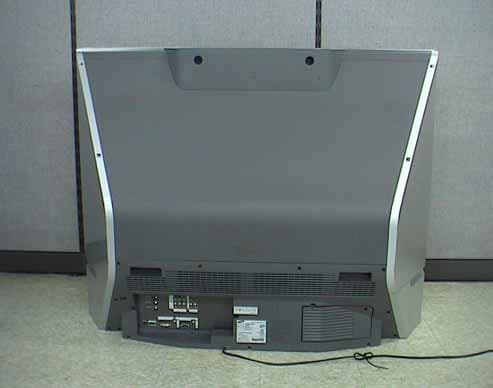
Click to zoom
Application Details
- Equipment Class
- JBP - Part 15 Class B Computing Device Peripheral
- Date of Grant
- Oct 10, 2004
- Application Purpose
- Original Equipment
- Date of Application
- Oct 10, 2004
- Equipment Note
- DLP Projection TV
- Company
- Samsung Electronics Co Ltd
- Country
- United States
Documents & Files
Document Text
Text extracted from the exhibit documents filed with the FCC. Open a document above to read the original.
Operational Description
JULY–SEPTEMBER199847 DIGITAL LIGHT PROCESSING—INTRODUCTION Digital Imaging (DI) began as a technology develop- ment program in 1992. The purpose was to find a use for the Digital Micromirror Device™ (DMD ™ ) and develop demonstration products that would attract customers to DI. Since the products were not intend- ed to go into production, little or no attention was paid to business process related to documenting requirements, verifying producibility or validating functionality. When it became evident that DI was a viable business in 1994, teams were established to define a business process model and a product devel- opment process. DI’s business process model The business process team was not interested in “reinventing the wheel” and began searching for suc- cessful existing models applicable to DI’s needs. TI’s Semiconductor Group (SC) model provided the basic structure for a non-end item product driven by mar- ket requirements. The TI calculator model provided the concept of a multi-layered market element. The DI team integrated the two models and released the Digital Imaging business process model in October 1994. As shown in Figure 1, business management and strategy development for DI’s products are driven by the needs of the market. The primary market inter- face is coordinated through the original equipment manufacturer (OEM). Demand assumptions are gen- erated on end-user needs. A product business model and work-share allocation between OEM and DI are established. Integrated product development efforts are coordinated to achieve full realization of market requirements and timely entry into the market. Sales and operations provide planning and support for product manufacturing and order fulfillment. To sup- port product design and build, a materiel team estab- lishes and manages supplier relationships and alliances. DI’s core technologies, driven by product strategy, have both evolutionary and revolutionary paths. Technology development is intended to lead product development to lower the risk of new tech- nology insertion into DI’s products. There are several enablers to this business model. Assessment of DI’s product quality, reliability and product safety are provided by an independent Quality Reliability Assurance (QRA) organization. Staffing and training of all DIers is handled through division-based Human Resources (HR) services. Legal Support Services manage all intellectual prop- erty and contractual issues. Information technology provides computer and tool infrastructure support Digital Imaging’s integrated product development process Abstract: The evolution of Digital Imaging (DI) from research and development to a product-oriented organiza- tion required additional discipline and focus on business processes. The high-level business map was defined to flow information from the marketplace requirements into the final product delivered to the customer. One of the critical pieces of the process flow was the product development process–translation of market and customer requirements into physical form. The product development process needed to be a dynamic document that met the needs of the organization. It needed to tightly couple the market requirements with the final product and ensure alignment to DI’s business strategies. A cross-functional team evaluated processes from inside and outside TI to limit the amount of effort the team would need to expend. The phase-gate process documented by DI covers product life cycle from concept to closeout in seven phases. The gates are business-focused reviews that evaluate progress, the project’s value proposi- tion and alignment with DI strategy. The latest improve- ment activity added details to the early phases, enabled use of Intranet access and increased consistency of prod- uct documentation and storage. Alice Parry, Bob Stoddard and Ron Barry 48TI TECHNICALJOURNAL DIGITAL LIGHT PROCESSING—INTRODUCTION and a networked environment to facilitate informa- tion sharing. Finance reports current status and fore- casts upward into TI’s corporate structure. It also provides support for financial risk assessments at the product level. Key business objectives drive process The business process model made it clear that the product development process must be driven by and aligned with DI business objectives. The product development team used the business model to clarify how development facilitated this flow and to help meet DI’s business objectives. With this process the customer is the center of DI’s focus. Customer satisfaction is the primary focus for DI. Part of the satisfaction quotient includes product- related business objectives such as: • Market driven product requirements • Meeting customers’ needs • Meeting time-to-market targets • Reducing product costs • Reducing product development cycle time • Improving product quality. Figure 2 shows a general information flow between customers and various DI organizational and func- tional entities. During the early phases of DI’s product develop- ment process, Marketing is responsible for identify- ing customer careabouts and translating them into market requirements. Systems Engineering creates the product specification and design requirements from the market requirements. Target product costs and time-to-market requirements also are established by Marketing. Proper market and systems analysis are critical to this process. Product Marketing’s presence as an inte- gral part of the product development team helps focus the development effort toward these objectives. The product development team, which includes man- ufacturing, tailors the process to meet the time-to- market window without sacrificing product quality. Product quality and reduction of product costs and cycle time are the responsibility of all functions including engineering, operations and QRA. Concurrent engineering during the requirements and design phases by engineering, manufacturing and customers, help to reduce the am…
Text truncated - open the document above for the full version.
Test Report
1 of 20 Samsung EMC Testing and Certification Laboratory Project No: LBE041846 This report shall not be reproduced except in full, without the written approval of SEC EMC Testing laboratory. EMC Test Report According to FCC Part 15 Subpart B Project No. LBE041846 Equipment under Test Applicant Samsung Electronics Co. Ltd; 416 Maetan-3 Dong, Paldal-Ku, Suwon City, Kyungki-Do, Korea, 442-742 FCC ID A3LAT56L5 Product Name DLP PROJECTION TV Model Name AT56L5 Manufacturer Samsung Electronics Co. Ltd Date of Test September 17 ~ 21, 2004 Issued Date September 21, 2004 Name/Position Signature Tested by Jang Tae Young Test Engineer Reviewed by No Cheon, Park Manager of EMC Lab. Authorized by Kyu Baek, Chung Chief of EMC Lab. 1. This test reports does not constitute an endorsement by NIST/NVLAP or U.S Government. 2. This test report is to certify that the tested device properly complies with the requirements of FCC Rules and Regulations Part 15 Subpart B Unintentional Radiators. All tests necessary to show compliance to the requirements were and these results met the specifications requirement. This laboratory is registered by the NIST/NVLAP, U.S.A. The test reported herein have been performed in accordance with its terms of registration. 2 of 20 Samsung EMC Testing and Certification Laboratory Project No: LBE041846 This report shall not be reproduced except in full, without the written approval of SEC EMC Testing laboratory. Table of Contents 1. General Information 1.1 Basic Information related Product 1.2 Detail Information related Product 1.3 Test Configuration 1.4 EUT Operating Conditions 1.5 Applied Standard 1.6 Test Facility 2. Summary of Test Results 3. Description of individual tests 3.1 Conducted Emission 3.2 Radiated Emission 4. Appendix 4.1 Test Photography 4.2 EUT Photography 3 of 20 Samsung EMC Testing and Certification Laboratory Project No: LBE041846 This report shall not be reproduced except in full, without the written approval of SEC EMC Testing laboratory. 1. General Information 1.1 Basic Information related Product Applicant Samsung Electronics Co. Ltd; Model name AT56L5 Applicant Address Samsung Electronics Co. Ltd; 416 Maetan3- Dong, Yeoung tong-Ku, Suwon City, Gyeonggi-Do, Korea, 443-742 Contact Person Kind of product DLP PROJECTION TV Valiant list None Manufacturer Samsung Electronics Co. Ltd; 1.2 Detail Information related Product Specification Resolution 1280 * 720 Horizontal Frequency 60kHz Vertical Frequency 75Hz 1.3 Operating Mode and Condition The system was configured for testing in typical fashion use. The mode of operation utilized for testing was selected to best simulate typical EUT use. - PC Video Input - PC DVI Input The EUT Exercise program used during radiated and conducted testing was designed to exercise the various system components in a manner similar to typical use. 1.4 Equipment Modifications No equipment modifications were required. 4 of 20 Samsung EMC Testing and Certification Laboratory Project No: LBE041846 This report shall not be reproduced except in full, without the written approval of SEC EMC Testing laboratory. 1.5 Test Procedure 1.5.1 Disturbance Voltage at Mains EUT was placed on a platform nominal size, 1m by 1.5m, raised 80cm above the conducti ng ground plane. The rear of tabletop was located 40cm to the vertical conducting groud plane. The rear of EUT, including peripherals was aligned and flush with rear of tabletop. All other surfaces of tabletop was at least 80cm from any other grounded conducing surface. I/O cables and AC cables that were connected to the peripherals were bundled in center. They were folded back and forth forming a bindle 30cm to 40cm long and were handed at a 40cm height to the ground plane. Each EUT current-carrying power lead, except the ground(safety)lead, were individually connected through a LISN to the input power source. All unused 50 ohm connectors of the LISN were resistively terminated in 50 ohm when not connected to the measuring equipment. 1.5.2 Radiated disturbance EUT was placed on a platform of nominal size, 1m by 1.5m, raised 80cm above the conducting ground plane. The rear of EUT, including peripherals was aligned and flush with rear of tabletop. I/O cables that were connected to the peripherals were bundle in center. They were folded back and forth forming a bundle 30cm to 40cm long and were hanged 40cm height to the ground plane. Test was made with the antenna positioned in both the horizontal and vertical planes of polarization. The measurement antenna was varied in height above the conducting ground plane and the run table azimuth was varied to obtain the maximum signal strength The system configuration, clock speed, mode of operation or video resolution, turntable azimuth with respect to the antenna were noted for each frequency found. The spectrum was scanned from 30 to 1000 MHz using biconiLog antenna. 5 of 20 Samsung EMC Testing and Certification Laboratory Project No: LBE041846 This report shall not be reproduced except in full, without the written approval of SEC EMC Testing laboratory. 1.6 Test Configuration Used EUT and Peripherals Seq Device Model Name Serial # Maker FCC ID/DoC A DLP Projection TV AT56L5 - SAMSUNG B PC M6050 812092FRC2822 SAMSUNG DoC C Printer ML-1750 - SAMSUNG A3LML1750 D PS/2 Keyboard 7800 K22115077 BTC Telecom DoC E PS/2 Mouse Scroll Mouse P801 01032707 SYE Systems FSUGMZFT Used Cable Description Connect Cable Length [m] Shielded [Y/N] Remark 1 Parallel (Printer) 1.7 Yes 2 Monitor 1.5 Yes 3 DVI 1.5 Yes 4 USB 1.5 Yes 5 PS/2 1.5 Yes 6 Component Video Out 1.5 No 7 AV front IN 1.5 No 8 Audio Out 1.5 No 9 S -Video Out 1.5 Yes 10 Audio Out 1.5 No 6 of 20 Samsung EMC Testing and Certification Laboratory Project No: LBE041846 This report shall not be reproduced except in full, without the written approval of SEC EMC Testing laboratory. Block Diagram 1.7 Applied Standards List Applied Standards Test Procedure FCC Part15 ANSI C63.4 : 2000 Performance Criteria A. normal perform…
Text truncated - open the document above for the full version.
Test Setup Photos
17 of 20 Samsung EMC Testing and Certification Laboratory Project No: LBE041846 This report shall not be reproduced except in full, without the written approval of SEC EMC Testing laboratory. 4. Appendix 4.1 Test Photography Pic. 1 Conducted Emission (Front) Pic. 2 Conducted Emission (Rear) 18 of 20 Samsung EMC Testing and Certification Laboratory Project No: LBE041846 This report shall not be reproduced except in full, without the written approval of SEC EMC Testing laboratory. Pic. 3 Radiated Emission (Front) Pic. 4 Radiated Emission (Rear)
Contact Information
Applicant
Jenni Chun(General Manager)
Technical Contact
PCTEST Engineering Lab., Inc.Randy Ortanez
[email protected]410-290-6652
6660-B Dobbin Road · Columbia, Maryland · United States
Test Firm
SAMSUNG ELECTRONICS CO., LTD.No Cheon Park
Technical Specifications
| # | Rule Parts | Frequency Range | Power Output |
|---|---|---|---|
| 1 | 15B | - | - |
Other Applications from Samsung Electronics Co Ltd
A3LSMS741B
Aug 05, 2026Portable Handset
Equipment Class
6VL - 15E 6 GHZ Very Low Power DeviceA3LSMX940
Jul 31, 2026BT,BLE Tablet DTS,UNII a,b,g,n,ac,ax,be and digitizer
Equipment Class
DTS - Digital Transmission SystemA3LSMS741U
Jul 30, 2026Portable Handset
Equipment Class
6CD - 15E 6 GHz Low Power Dual ClientA3LSMX840
Jul 27, 2026BT,BLE Tablet DTS,UNII a,b,g,n,ac,ax and Digitizer
Equipment Class
DSS - Part 15 Spread Spectrum TransmitterA3LSMX848U
Jul 27, 2026WCDMA, LTE, 5G NR Tablet BT,BLE, DTS,UNII a b g n ac ax and Digitizer
Equipment Class
JBP - Part 15 Class B Computing Device Peripheral