A3LBTW2002 Channel Audio Transmitter
Samsung Electronics Co Ltd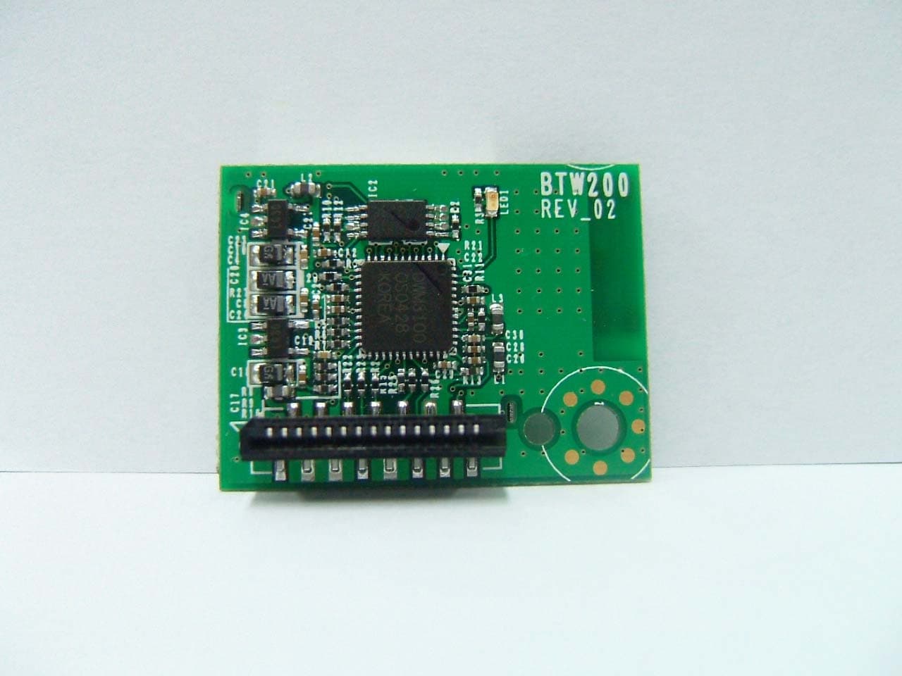
Click to zoom
Application Details
- Equipment Class
- DSS - Part 15 Spread Spectrum Transmitter
- Date of Grant
- Mar 07, 2005
- Application Purpose
- Original Equipment
- Date of Application
- Mar 07, 2005
- Equipment Note
- 2 Channel Audio Transmitter
- Frequency Range
- 2402.00000000 - 2480.00000000
- Company
- Samsung Electronics Co Ltd
- Country
- United States
Documents & Files
Document Text
Text extracted from the exhibit documents filed with the FCC. Open a document above to read the original.
Users Manual
SPECIFICATION FOR APPROVAL Customer: Address: Issue No. Part No. BTW200 Description: Manufacturer Samsung Electronics Huizhow CO., LTD. Vendor: Approved by: BLUE TEK CO., LTD. Approved Date: MM/DD/YY: 01/ 03 /2005 BLUE TEK CO., LTD. 416, Maetan-3Dong, Paldal-Gu, Suwon City, Kyungki-Do, Korea 442-742 TEL: +82-31-200-8672 FAX:+82-31-200-4390 http://www.bluetek.co.kr Abbreviations . ADC: Analog to Digital Converter . AGC: Automatic Gain Control . ANT: Antenna . BBP: Base Band Processor . bps : Bit per second . BT : Bluetooth . DAC: Digital to Analog Converter . FHSS : Frequency Hopping Spread Spectrum . GFSK : Guassian Frequency Shift Keying . ID : Identification . I/O: Input/Output . ISM: Industrial Scientific Medical Frequency Band . LDO: Low Drop Out Regulator . LNA: Low Noise Amplifier . L/R : Left/Right . MCU: Micro Process Unit . PA: Power Amplifier . PCM : Pulse Code Modulation . RF: Radio Frequency . SAW: Surface Acoustic Wave . SMD: Surface Mounted Device . Tx : Transmitter . Rx : Receiver . 1. Introduction This document is manual for BTW200 module. BTW200 module is for sending & receiving audio data without wire. Transmission methods are FHSS(Frequency Hopping Spread Spectrum) which is used in bluetooth technology. BTW200 is composed of two parts. One is Tx module and the other is Rx module. Tx module is works for master, which receives and compresses audio signal at baseband chip and sending signal without wire. Rx module is works for slave, which receives signal without wire. The both modules can send and receive data each other. This system is for sending and receiving wireless digital data with CD audio quality. The following characteristics are for satisfying quality. - Bluetooth RF chip is used for RF function without wire. - DWM3100 supports audio interface, works for compressing & decompressing and controls audio codec & RF modem chip. - Real-time sending and receiving are available. - It could works independently without S/W control. To loading parameter for operating DWM3100 when you turning on the power, Booting EEPROM(128 bytes or 256 bytes) is implemented on set. In addition, I2C mater function is included for accessing EEPROM. - There is another interface for testing system, additional data interface and controlling other system. - CD audio quality is available. - Data transmission is possible. - Can avoid interference with other wireless products. - Operation clock and master clock are used. 32MHz clock for baseband part and RF 2. Standard and general specification 2.1 Standard Specification - 1Mbps high quality audio data communication - FHSS - 2.4GHz ISM band 2.2 General Specification Description Value UnitRemark Frequency range 2,402 ~ 2,480 MHz Antenna impedance 50 ohmRefer to the specification of antenna. Data communication Half duplex Frequency type F2D [Specification of antenna] - Tx Antenna Specification Electrical Specification Frequency Range 2402 ~ 2480 MHz V.S.W.R 1.6: 1 (max) Gain(Max) 1.6 dBi Nominal Impedance 50 ohm Polarization Linear Mechanical Specification Dimensions 12.8*3.9*1.1 Weight 0.1g Radiator Copper Operating Temp -40 ~ 85 Operating Humidity 10 ~ 90 % Option SMD 2.3 Electrical Specification Description Value Unit Remark Communication rate 1 Mbps Output power <10mW/1MHz -36 dBm 30MHz~1GHz -30 dBm 1 to 12.75MHz -40 dBm 1.8 to 1.9GHz Out-of-Band Spurious -40 dBm 5.15 to 5.3GHz Modulation Spectrum spreading Frequency deviation < ±50 x 10 -6 Maximum input level -20 dBm @FER: 8Frame/1m Tx module 65 mA Typ. Current consumption Rx module 65 mA Typ. Bandwidth < 1MHz Bandwidth 2.4 Environmental Specification Description Value Unit Remark Operating temperature -10 ~ +50 °C Storage temperature -20 ~+80 °C Humidity (Non-condensing) 10 ~ 90 % 2.5 Mechanical Specification Description Value Unit Remark Tx module 32 x 24 x 10 mm Dimensions Rx module 32 x 24 x 10 mm Weight 4.1 g 3. Structure 3.1 Diagram Transceiver module is consist of digital block and RF block. Digital block is for controlling signal and RF block is for connecting wireless signal. [Top] [Bottom] 3.2 PCB Profile The PCB of transceiver is 4 layers and following is detailed information. z PCB material: RCC and FR-4 z PCB Layer: 4 layer Impedance Board z PCB Size: Tx Module -Æ 32 mm(L) × 24 mm(W) × 10 mm(T) Rx Module -Æ 32mm(L) × 24 mm(W) × 10 mm(T) Regulatory Information FCC compliance Information This device complies with part 15 of FCC Rules. Operation is subject to the following two conditions: 1. This device may not cause harmful interference, and 2. This device must accept any interference received. Including interference that may cause undesired operation. Information to User This equipment has been tested and found to comply with the limits for a Class B digital device, Pursuant to part 15 of the FCC Rules. These limits are designed to provide reasonable protection against harmful interference in a residential installation. This equipment generates, uses and can radiate radio Frequency energy and, if not installed and used in accordance with the instructions, may cause harmful interference to radio communications. However, there is no guarantee that interference will not occur in a particular installation. If this equipment does cause harmful interference to radio or television reception, which can be determined by turning the equipment off and on, the user is encouraged to try to correct the interference by one or more of the following measures: - Reorient or relocate the receiving antenna. - Increase the separation between the equipment and receiver - Connect the equipment into an outlet on a circuit different from that to which the receiver is connected. - Consult the dealer or an experienced radio/TV technician for help. FCC WARNING: This equipment may generate or use radio frequency energy. Changes or modifications to this equipment may cause harmful interference unless the modifications are expressly approved in the instruction manual. The user could lose the authority to operat…
Text truncated - open the document above for the full version.
Users Manual
Regulatory Information FCC compliance Information This device complies with part 15 of FCC Rules. Operation is subject to the following two conditions: 1. This device may not cause harmful interference, and 2. This device must accept any interference received. Including interference that may cause undesired operation. Information to User This equipment has been tested and found to comply with the limits for a Class B digital device, Pursuant to part 15 of the FCC Rules. These limits are designed to provide reasonable protection against harmful interference in a residential installation. This equipment generates, uses and can radiate radio Frequency energy and, if not installed and used in accordance with the instructions, may cause harmful interference to radio communications. However, there is no guarantee that interference will not occur in a particular installation. If this equipment does cause harmful interference to radio or television reception, which can be determined by turning the equipment off and on, the user is encouraged to try to correct the interference by one or more of the following measures: - Reorient or relocate the receiving antenna. - Increase the separation between the equipment and receiver - Connect the equipment into an outlet on a circuit different from that to which the receiver is connected. - Consult the dealer or an experienced radio/TV technician for help. FCC WARNING: This equipment may generate or use radio frequency energy. Changes or modifications to this equipment may cause harmful interference unless the modifications are expressly approved in the instruction manual. The user could lose the authority to operate this equipment if an unauthorized change or modification is made.
Cover Letter(s)
516-229, Chen Jiang Town, Huizhou-City, Guangdong-Province, China March 8, 2005 Federal Communications Commission Equipment Authorization Branch 7435 Oakland Mills Road Columbia, MD 21046 Re: FCC ID: A3LBTW200 To whom it may concern: Submitted herewith is an application for a 2ch Audio Transceiver modular. In accordance with the requirements set forth in DA 00-1407 Released: June 26, 2000, this device incorporates the design features as described and listed below for Part 15 modular transmitter approval: 1. The modular transmitter has its own RF shielding. As can be seen from the test site photos, the device was tested outside the host equipment that provided data and power to the unit. 2. This modular transmitter has buffered modulation/data inputs that ensure the module will comply with Part 15 requirements under conditions of excessive data rates or over-modulation. 3. This modular transmitter has its own power supply regulation to ensure that the module will comply with Part 15 requirements regardless of the design of the power supplying circuitry in the device into which the module is installed. 4. The modular transmitter complies with the antenna requirements of Section 15.203 and 15.204(c). It is permanently attached to the printed circuit board as shown in the photos. 5. This modular transmitter was tested in a stand-alone configuration outside the host device during testing. The host device is a battery-powered unit intended to be used as a mobile bar code reader. No modifications were made to the host device. 6. This modular transmitter is labeled with its own FCC ID number, and, if the FCC ID is not visible when the module is installed inside another device, then the outside of the device into which the module is installed will also display a label referring to the enclosed module. This exterior label will use this wording: “Contains FCC ID: A3LBTW200”. 7. This modular transmitter complies with all operating requirements applicable to the transmitter. 8. This modular transmitter complies with applicable RF exposure requirements. Its maximum EIRP is 78 mW and the antenna is mounted inside the module enclosure. Further, the module is intended to be installed inside a host device which provides additional isolation from the user. Specific installation and operating instructions for users, installers and other interested parties are provided to ensure compliance. 9. This modular transmitter will be installed by OEM and will be used only for the Home Theater Products of SAMSUNG Electronics Co. LTD. Sincerely, O-Won Seo R&D Management Group /Manager
Cover Letter(s)
516-229, Chen Jiang Town, Huizhou-City, Guangdong-Province, China BTW200 Declaration Per FCC 15.247 Requirements 1 Output power and channel separation: BTW200 is standard module to deliver 2channel Stereo audio in 2.4GHz frequency band. This device follows 15.247 category about the definition of frequency hopping device. There is only one transmitter which is driven by identical input parameters concerning these two parameters. Only a different hopping sequence will be used. For this reason the check of these RF parameters in one op-mode is sufficient. 2 Frequency range of a Bluetooth device: Hereby we declare that the maximum frequency of this device is 69Channels between 2,402 ~ 2,480 MHz.(excluded 2,402 / 2,410 / 2,418 / 2,426 / 2,434 / 2,442 / 2,450 / 2,458 / 2,466 / 2,474MHz). This band is permitted ISM band by Federal Communication Committee of US. 3 Co-ordination of the hopping sequence in data mode to avoid simultaneous occupancy by multiple transmitters: Each BTW200 device which want to communicate with other units must contain the same 28bit digital ID. Based on this digital ID, each device randomly calculates and stores the hop sequence by itself. 4 Example of a hopping sequence in data mode: Example of a BTW200’s 69 hopping sequence 21, 44, 23, 53, 46, 55, 48, 33, 52, 35, 50, 65, 54, 67, 37, 60, 39, 58, 69, 62, 71, 25, 68, 27, 66, 57, 70, 59, 29, 76, 31, 74, 61, 78, 63, 01, 41, 05, 43, 03, 73, 07, 09, 45, 13, 47, 11, 77, 15, 49, 66, 53, 68, 02, 70, 06, 01, 51, 03, 55, 05, 04 5 Receiver input bandwidth and behaviors for repeated single or multiple packets: The input bandwidth of the receiver is 1 MHz. In every connection, there is one Transmitter and the other one is the Receiver. The Transmitter determines the hopping sequence randomly. The slave follows this sequence. Both devices shift between Tx and Rx time slot according to the clock of the master. The Transmitter adapts its hopping frequency and its Tx/Rx timing according to the packet type of the connection. Also the Receiver of the connection will use these settings. Repeating of a packet has no influence on the hopping sequence. The hopping sequence generated by the Transmitter of the connection will be followed in any case. That means, a repeated packet will not be send on the same frequency, it is send on the next frequency of the hopping sequence. 6 Dwell time in data mode Dwell time(The average time of occupancy) on any channel shall not be greater than 0.4 seconds(400ms) within a period of 0.4 seconds multiplied by the number of hopping channels employed. Based on above information: Dwell time = (3 X 575us X 400 + 575us X 400) / (69 hopping channels*400us) = 0.033ms 7 Channel Separation The nominal channel spacing of BTW200 is 1Mhz independent of the operating mode. The maximum “initial carrier frequency tolerance” is fcenter = 75 kHz. This was checked for three frequencies (2403, 2443, 2480 MHz). Additionally an example for the channel separation is given in the test report 8 Receiver input bandwidth and synchronization in hybrid mode: The receiver input bandwidth is 1 MHz. When two BTW200 devices establish connection for the first time, one device sends an SEEK signal, the other device is scanning for this SEEK signal. If two devices loose connection, repeat same procedure as above. 9 Equally average use of frequencies in data mode and behavior for short transmissions: Each Frame is 2.5ms. 4Slots consists of One Frame. There is 3 Tx Slot an 1 Rx Slot. Each Slot is 575uS. Sequentially, 3 Tx and 1Rx have been repeated. Sincerely, O-Won Seo R&D Management Group /Manager
Cover Letter(s)
516-229, Chen Jiang Town, Huizhou-City, Guangdong-Province, China February 2, 2005 Federal Communications Commission Equipment Authorization Branch 7435 Oakland Mills Road Columbia, MD 21046 In re : SAMSUNG Electronics Huizhou Co., Ltd. FCC ID : A3LBTW200 15.19 statement request Gentlemen: Because The device is so small that it is not practicable to place the statement specified under 15.19 statement request, the information required by this paragraph shall be placed in a prominent location in the user's manual. Sincerely, O-Won Seo R&D Management Group /Manager
Cover Letter(s)
516-229, Chen Jiang Town, Huizhou-City, Guangdong-Province, China February 2, 2005 Federal Communications Commission Equipment Authorization Branch 7435 Oakland Mills Road Columbia, MD 21046 LETTER OF AUTHORIZATION To whom it may concern: We, the undersigned, hereby authorize DIGITAL EMC Co., Ltd., to act on our behalf in all manners relating to application for equipment authorization for FCC ID: A3LBTW200. Including signing of all documents relating to these matters. Any and all acts carried out by DIGITAL EMC Co., Ltd., on our behalf shall have the same affect as acts of our own. This authorization is valid until further written notice from SAMSUNG Electronics Huizhou Co., Ltd. Sincerely, O-Won Seo R&D Management Group /Manager
Cover Letter(s)
516-229, Chen Jiang Town, Huizhou-City, Guangdong-Province, China February 2, 2005 Federal Communications Commission Equipment Authorization Branch 7435 Oakland Mills Road Columbia, MD 21046 In re : SAMSUNG Electronics Huizhou Co., Ltd. FCC ID : A3LBTW200 Request for Confidentiality Gentlemen: In accordance with 0.459 of CFR 47, SAMSUNG Electronics Huizhou Co., Ltd. hereby requests confidentiality of the Block diagram, Schematics, Parts list, Operational Description attachments for the subject application. These documents contain detailed system and equipment description and related information about the product which SAMSUNG Electronics Huizhou Co., Ltd. considers to be proprietary, confidential, and a custom design and, otherwise, would not release to the general public. Since this design is a basis from which future technological products will evolve, SAMSUNG Electronics Huizhou Co., Ltd. considers that this information would be of benefit to its competitors, and that the disclosure of the information in these documents would give competitors an unfair advantage in the market. Sincerely, O-Won SEO R&D Management Group /Manager
External Photos
View 1
External Photos
Fixed DVD Receiver FCC ID: A3LBTW200 Fixed rear amplifier FCC ID: A3LBTW200
ID Label/Location Info
FCC ID: A3LBTW200 Copyright ○ c 2005, DIGITAL EMC Co., Ltd. Additional Label and locations which will be located on the outside of the device into which this modular transmitter will be installed FCC ID: A3LBTW200 Copyright ○ c 2005, DIGITAL EMC Co., Ltd.
ID Label/Location Info
DEMC#DR50110502A Copyright ○ c 2005, DIGITAL EMC Co., Ltd. FCC ID SAMPLE LABEL & LOCATION LABELLING REQUIREMENTS PER §2.925 The Label shown shall be permanently affixed at a conspicuous location on the device and be readily visible to the user at the time of purchase FCC ID: A3LBTW200 IC:649E-BTW200 DEMC#DR50110502A Copyright ○ c 2005, DIGITAL EMC Co., Ltd. APPENDIX Model Name
Internal Photos
View 1 View 2 View 3
Operational Description
Product Specification Product Specification Rufa 2.4 GHz SMD Antenna Rev : AE020157-F / April 30 2004 Rufa 2.4 GHz SMD Antenna 2 (10)Subject to changes without prior notice 1. FEATURES - Designed for 2.4 GHz applications [Bluetooth TM , WiFi TM (802.11b/g), Zigbee TM , WiMedia TM etc.] - Intended for SMD mounting - Supplied in tape on reel 2. DESCRIPTION - Mobile phones - PDAs - Headsets - Laptops - PC- Cards - CF- Cards 3. APPLICATION The Rufa antenna is intended for use with all 2.4 GHz applications. The antenna requires a groundplane, i.e your device acts as an active part of the antenna and thus demand careful consideration concerning its placement TABLE OF CONTENT 1. Features ......................................................................................................................................................................... 2 2. Description ..................................................................................................................................................................... 2 3. Application ...................................................................................................................................................................... 2 4. Model names .................................................................................................................................................................. 3 5. General data ................................................................................................................................................................... 3 6. Electrical characteristics ................................................................................................................................................. 3 7. Electrical performance .................................................................................................................................................... 4 7.1 Voltage Standing Wave Ratio ............................................................................................................................... 4 7.2 3D-Radiation ........................................................................................................................................................ 4 7.3 Radiation patterns ................................................................................................................................................ 4 8. Antenna Dimensions ....................................................................................................................................................... 5 9. Antenna Foot print .......................................................................................................................................................... 5 10. Electrical interface ........................................................................................................................................................ 6 10.1 Transmission line and matching ......................................................................................................................... 6 10.2 Test board dimensions ....................................................................................................................................... 6 10.3 Test board matching ........................................................................................................................................... 6 11. Soldering ....................................................................................................................................................................... 6 11.1 Recommended soldering conditions .................................................................................................................. 6 11.2 Leadfree soldering ............................................................................................................................................. 6 12. Reliability ...................................................................................................................................................................... 7 12.1 Temperature and Humidity ................................................................................................................................. 7 12.2 Mechanical ......................................................................................................................................................... 7 12.3 Miscellaneous .................................................................................................................................................... 7 12.4 Judgement standard .......................................................................................................................................... 7 13. Hazardous Material Reguration Conformance .............................................................................................................. 7 14. Application example ...................................................................................................................................................... 8 15. Packaging ..................................................................................................................................................................... 9 15.1 Shelf storage recommendation .......................................................................................................................... 9 15.2 Tape characteristics ........................................................................................................................................... 9 15.3 Reel dimension .................................................................................................................................................. 9 15.4 Box dimensions ................................................................................................................................…
Text truncated - open the document above for the full version.
Operational Description
ATTACHMENT FCC ID: A3LBTW200 ** MPE Calculations ** The EUT will only be used with a separation of 20 centimeters or greater between the antenna and the body of the user. The MPE calculation for this exposure is shown below. The peak radiated output power (EIRP) is calculated as follows: EIRP = P + G EIRP = 14.50 dBm + 4.4 dBi EIRP = 18.9 dBm Where, P = Power input to the antenna (mW) G = Power gain of the antenna (dBi) Power density at the specific separation: S = PG/(4R 2 π) S = (28.18 * 2.8) / (4 * 20 2 * π) S = 0.0157 mW/cm 2 Where, S = Maximum power density (mW/cm 2 ) P = Power input to the antenna (mW) G = Numeric power gain of the antenna R = Distance to the center of the radiation of the antenna (20cm = limit for MPE) The Maximum permissible exposure (MPE) for the general population is 1 mW/cm 2 . The power density at 20cm does not exceed the 1 mW/cm 2 limit. Therefore, the exposure condition is compliant with FCC rules. Estimated safe separation: R = √(PG / 4π) R = √(28.18 * 2.8 / 4π) R = 2.51 cm Where, P = Power input to the antenna (mW) G = Numeric power gain of the antenna R = Distance to the center of the radiation of the antenna (20cm = limit for MPE) The numeric gain(G) of the antenna with a gain specified in dB is determined by: G = Log -1 (dB antenna gain / 10) G = Log -1 (4.4 / 10) G = 2.8
Test Report
DEMC#DR50110502A Copyright ○ c 2005, DIGITAL EMC Co., Ltd. Page 1 of 32 683-3, Yubang-Dong, Yongin-Si, Kyunggi-Do, Korea. 449-080 Tel: +82-31-321-2664 Fax: +82-31-321-1664 http://www.digitalemc.com CERTIFICATION OF COMPLIANCE Samsung Electronics Huizhou Co., Ltd. 516-229 Chen Jiang Town, Huizhou-City, Guangdong- Province, China. Dates of Tests: January 12 ~ 27,2005 Test Report S/N: DR50110502A Test Site : DIGITAL EMC CO., LTD. FCC ID APPLICANT FCC Classification : FHSS Sequence Spread Spectrum (FHSS) Device name : 2ch Audio Transceiver Manufacturer : Samsung Electronics Huizhou Co., Ltd Model name : BTW200 Test Device Serial number : Identical prototype FCC Rule Part(s) : FCC Part 15.247 Subpart C; ANSI C-63.4-2001 Frequency Range : 2402 ~ 2480 MHz Max. Output power : 0.028 W Conducted Data of issue : January 30, 2005 I attest to the accuracy of data. All measurements reported herein were performed by me or were made under my supervision and are correct to the best of my knowledge and belief. I assume full responsibility for the completeness of these measurements and vouch for the qualifications of all persons taking them. A3LBTW200 Samsung Electronics Huizhou Co., Ltd. DEMC#DR50110502A Copyright ○ c 2005, DIGITAL EMC Co., Ltd. Page 2 of 32 TABLE OF CONTENTS 1. GENERAL INFORMATION’S -------------------------------------------------------------------------- 2. INFORMATION’S ABOUT TEST ITEM ------------------------------------------------------------- 3. TEST REPORT --------------------------------------------------------------------------------------------- 3.1 SUMMARY OF TESTS ------------------------------------------------------------------------------ 3.2 TRANSMITTER REQUIREMENTS --------------------------------------------------------------- 3.2.1 CARRIER FREQUENCY SEPARATION ---------------------------------------------------- 3.2.2 NUMBER OF HOPPING FREQUENCIES -------------------------------------------------- 3.2.3 20 dB BANDWIDTH ---------------------------------------------------------------------------- 3.2.4 TIME OF OCCUPANCY (Dwell Time) ------------------------------------------------------- 3.2.5 PEAK OUTPUT POWER ----------------------------------------------------------------------- 3.2.6 BAND - EDGE (at 20 dB blow) ---------------------------------------------------------------- 3.2.7 OUT OF BAND EMISSION - RADIATED -------------------------------------------------- 3.2.8 AC CONDUCTED EMISSIONS -------------------------------------------------------------- 3.3 RECEIVER REQUIREMENTS --------------------------------------------------------------------- 3.3.1 AC CONDUCTED EMISSIONS -------------------------------------------------------------- 3.3.2 OUT OF BAND EMISSION - RADIATED -------------------------------------------------- ANNEX TEST EQUIPMENT USED FOR TESTS ---------------------------------------------------- 3 4 5 5 6 6 8 11 14 16 19 26 27 28 28 29 30 DEMC#DR50110502A Copyright ○ c 2005, DIGITAL EMC Co., Ltd. Page 3 of 32 1. General information’s This report contains the result of tests performed by: DIGITAL EMC CO., LTD. Address : 683-3, Yubang-Dong, Yongin-Si, Kyunggi-Do, Korea. 449-080 http://www.digitalemc.com E-mail : [email protected] Tel: +82-31-321-2664 Fax: +82-31-321-1664 Quality control in the testing laboratory is implemented as per ISO/IEC 17025 which is the “General requirements for the competents of calibration and testing laboratory”. This laboratory is accredited by NVLAP for NVLAP Lab. Code : 200559-0. Test operator: engineer January 30, 2005 Won -Jong LEE Data Name Signature Report Reviewed By: Technical Director January 30, 2005 Harvey Sung Data Name Signature Ordering party: Company name : Samsung Electronics Huizhou Co., Ltd. Address : Chen Jiang Town, Guangdong-Province, Zip code : 516-229 City/town : Huizhou-City Country : China Date of order : January 12, 2005 DEMC#DR50110502A Copyright ○ c 2005, DIGITAL EMC Co., Ltd. Page 4 of 32 2. Information’s about test item A3LBTW200 2.1 Equipment information Equipment model name BTW200 Type of equipment Bluetooth Module Frequency band 2402 ~ 2480 MHz Type of Modulation GFSK Channel Spacing 1.0 MHz Type of antenna Chip Antenna (Max. Gain: 4.4dBi) Power DC 5 V by main system 2.2 Tested frequency Frequency TX RX Low frequency 2402MHz 2402MHz Middle frequency 2441MHz 2441MHz High frequency 2480MHz 2480MHz 2.3 Tested environment Temperature : 15 ~ 35 ( o C) Relative humidity content : 20 ~ 75 % Air pressure : 86 ~ 103 kPa Details of power supply : 5 VDC (powered by power supply) 2.4 EMI Suppression Device(s)/Modifications EMI suppression device(s) added and/or modifications made during testing -> none DEMC#DR50110502A Copyright ○ c 2005, DIGITAL EMC Co., Ltd. Page 5 of 32 3. Test Report 3.1 Summary of tests FCC Part Section(s) Parameter Limit Test Condition Status (note 1) I. Transmit mode(Tx) Carrier Frequency Separation > 25 kHz C Number of Hopping Frequencies > 75 hops C 20 dB Bandwidth < 1 MHz C 15.247(a) Dwell Time 0.4 seconds within a 30 second period per any frequency C 15.247(b) Transmitter Output Power < 1Watt C Band-edge (or Occupied BW for IC) 2400 < f < 2483.5 MHz C 15.247(c) Out of Band Emissions (Bandwidth at 20 dB blow) The radiated emission to any 100 kHz of outband shall be at least 20dB below the highest inband spectral density. Conducted C 15.205 15.209 General Field Strength Limits (Restricted Bands and Radiated Emission Limits) < FCC 15.209 limits Radiated C 15.207 AC Conducted Emissions EN 55022 Line Conducted NA II. Recei…
Text truncated - open the document above for the full version.
Contact Information
Applicant
Jenni Chun(General Manager)
Test Firm
DT&C Co.,Changho Lee
Technical Specifications
| # | Rule Parts | Frequency Range | Power Output |
|---|---|---|---|
| 1 | 15C | 2.40 GHz - 2.48 GHz | 28.00 mW |
Other Applications from Samsung Electronics Co Ltd
A3LSMS741B
Aug 05, 2026Portable Handset
Equipment Class
6VL - 15E 6 GHZ Very Low Power DeviceA3LSMX940
Jul 31, 2026BT,BLE Tablet DTS,UNII a,b,g,n,ac,ax,be and digitizer
Equipment Class
DTS - Digital Transmission SystemA3LSMS741U
Jul 30, 2026Portable Handset
Equipment Class
6CD - 15E 6 GHz Low Power Dual ClientA3LSMX840
Jul 27, 2026BT,BLE Tablet DTS,UNII a,b,g,n,ac,ax and Digitizer
Equipment Class
DSS - Part 15 Spread Spectrum TransmitterA3LSMX848U
Jul 27, 2026WCDMA, LTE, 5G NR Tablet BT,BLE, DTS,UNII a b g n ac ax and Digitizer
Equipment Class
JBP - Part 15 Class B Computing Device Peripheral