A3LDNUBS1WLAN Transmitter Module
Samsung Electronics Co Ltd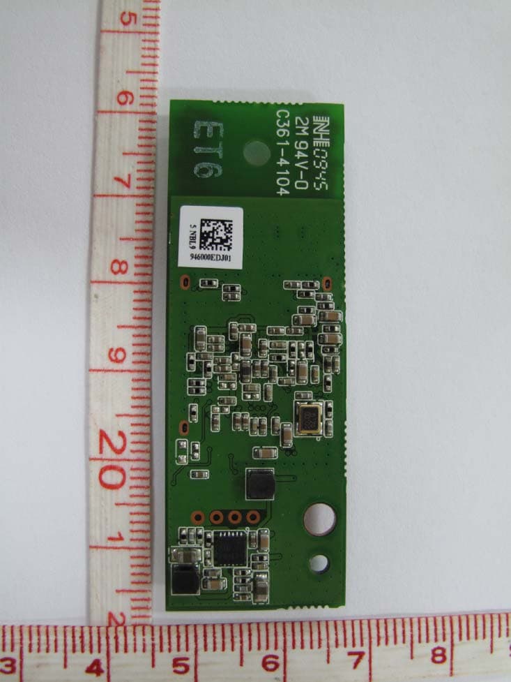
Click to zoom
Application Details
- Equipment Class
- DTS - Digital Transmission System
- Date of Grant
- Apr 05, 2010
- Application Purpose
- Original Equipment
- Date of Application
- Apr 05, 2010
- Equipment Note
- WLAN Transmitter Module
- Frequency Range
- 2422.00000000 - 2452.00000000
- Company
- Samsung Electronics Co Ltd
- Country
- United States
Documents & Files
Document Text
Text extracted from the exhibit documents filed with the FCC. Open a document above to read the original.
Users Manual
User manual Product description: IEEE 802.11g/n 2x2 USB module WNC model name: DNUB-S1 Samsung model name: DNUBS1 Version: V2.0 Networking Product Center Wistron Neweb ® Corporation No. 10-1, Lin-hsin I Road, Science-Based Industry Park, Hsinchu 300, Taiwan, R.O.C. Tel: +886-3-666-7799 Fax:+886-3-666-7711 Subject to change without notices © Copyrights 2009 by Wistron Neweb ® All rights reserved DNUB-S1 delivery specification 1. Introduction DNUB-S1 is a USB embedded module compliant with IEEE802.11n Draft 2.0 standard. The core chipset is from Broadcom, part number BCM43231. 2. Features 2x2 MIMO technology Data rates up to 130Mbps for 20MHz channels and 300Mbps for 40MHz channels Designs meet Pb-free/RoHS worldwide requirements Integrated ARM® Cortex-M3™ CPU and on-chip RAM for USB host offload Single driver across platforms simplifies driver update process and improves customer satisfaction WPA™/WPA2™ Cisco® Compatible Extensions (CCXv4, CCXv5) Full-rate AES engine in hardware WMM® for quality of service Integrated 2.4G Power Amplifier (BCM43231) provides path to lower solution cost for single-band designs Support for Windows® XP, Windows Vista®, and Linux® Operating Systems USB AP functionality provides 802.11n dual-band upgrade path to legacy routers and gateways LED reserved for special application. DNUB-S1 delivery specification 3. Hardware Architecture: 3.1 Main Chipset Information Item Vender Part number MAC/BBP/Radio Transceiver/PA Broadcom BCM43231 3.2 Circuit Block Diagram The major internal components and external interfaces of DNUB-S1 are illustrated in Figure 1-1. JTAG USB 2.0 GPIO Internal Bus ARM ROM RAM Draft 802.11n MAC Securuty SPROM I/F Dra ft- 802.11n PHY 2x2 Ra dio BCM43231 Figure 1-1 DNUB-S1 Major Component and System Interface 3.3 Outlook Diagram To p v i e w LED option (default was removed) Two options for USB connector ( FPC & cable) Antenna 0 Antenna 1 Fix hole for plastic screw (Metal screw will impact the antenna performance) Fix hole for screw DNUB-S1 Bottom view 3.4 Antennas Information Two trace antennas supporting both TX & RX. 3.4..1 VSWR ANT 1 ANT 0 DNUB-S1 3.4.2 Antenna Pattern DNUB-S1 3.4.3 Efficiency The efficiency is 35%. 3.4.4 Gain Table XY plan XZ plan YZ plan 2400 -3.03 -0.09 -1.32 2450 -2.15 0.23 -0.58 2500 -1.89 0.6 0.33 Peak gain (dBi) MHz 4. Interface definition GND GND D+ D- VCC DNUB-S1 USB FPC Cable & connector DNUB-S1 5. Mechanical drawing 5.1 Dimension DNUB-S1 6. Specifications: 6.1 Supply Voltage: 5V±5% DC 6.2 Current Consumttion Unit (Typical level, with +/- 50mA tolerance) 390 HT20 Tx MCS8 HT20 Tx MCS15 Condition 5V supply only 11b TX mode@16dBm 11g TX mode@15dBm 11b Throughput . Tx HT40 Tx MCS8580 550 mA HT40 Tx MCS15 390 170 420 11g Throughput . Tx Associated and idle with power saving Peak 265 260 400 6.3 RF power (Typical power level per chain with +/- 2.5 dB tolerance ) ( unit:dBm ) 24122437247224122437 2472 1Mbps 161616 HT40MCS0 13.513.513.5 2Mbps 161616 HT40MCS1 13.513.513.5 5.5Mbps 161616 HT40MCS2 13.513.513.5 11Mbps 161616 HT40MCS3 13.513.513.5 6Mbps 151515 HT40MCS4 13.513.513.5 9Mbps 151515 HT40MCS5 13.513.513.5 12Mbps 151515 HT40MCS6 13.513.513.5 18Mbps 151515 HT40MCS7 13.513.513.5 24Mbps 151515 36Mbps 151515 48Mbps 151515 54Mbps 151515 HT20MCS0 13.513.513.5 HT20MCS1 13.513.513.5 ` HT20MCS2 13.513.513.5 HT20MCS3 13.513.513.5 HT20MCS4 13.513.513.5 HT20MCS5 13.513.513.5 HT20MCS6 13.513.513.5 HT20MCS7 13.513.513.5 20MHz BW MHz 40MHz BW MHz DNUB-S1 Notes: Power level for different country domains is country dependent and Broadcom driver & SPROM will control the regulatory power table. Therefore, the actual power may be lower than this number. 6.4 RF Sensitivity (Typical sensitivity level, 2RX with +3/- 6 dB tolerance) ( unit:dBm ) 24122442247224122442 2472 1Mbps -98-98-98 HT40 MCS0 -89-89-89 2Mbps -96-96-96 HT40 MCS1 -88-88-88 5.5Mbps -93-93-93 HT40 MCS2 -86-86-86 11Mbps -89-89-89 HT40 MCS3 -82-82-82 6Mbps -91-91-91 HT40 MCS4 -80-80-80 9Mbps -90-90-90 HT40 MCS5 -74-74-74 12Mbps -89-89-89 HT40 MCS6 -73-73-73 18Mbps -88-88-88 HT40 MCS7 -71-71-71 24Mbps -86-86-86 36Mbps -83-83-83 48Mbps -77-77-77 54Mbps -76-76-76 HT20 MCS0 -92-92-92 HT20 MCS1 -91-91-91 HT20 MCS2 -90-90-90 HT20 MCS3 -85-85-85 HT20 MCS4 -83-83-83 HT20 MCS5 -77-77-77 HT20 MCS6 -76-76-76 HT20 MCS7 -74-74-74 MHz 20MHz BW MHz 40MHz BW 6.5 Environmental Spec. Operating Temperature Range: 0degree C~ 60degree C Storage Temperature Range: Temperature: -20~80°C Humidity: 95%(MAX) Operating Humidity Range: 10%~90% (No dew condensation) DNUB-S1 7. NOTICE FCC ID: A3LDNUBS1 NOTICE In accordance with FCC Part 15, the A3LDNUBS1 is listed as a Modular Transmitter device. End products that include the A3LDNUBS1 shall have the words “Contains Transmitter module FCC ID: A3LDNUBS1” on an exterior label l. This device complies with Part 15 of FCC Rules. Operation is Subject to following two conditions: (1) This device may not cause harmful interference, and (2) This device must accept any interference received including interference that cause undesired operation. This equipment has been tested and found to comply within the limits for a Class B digital device, pursuant to part 15 of the FCC Rules. These limits are designed to provide reasonable protection against harmful interference in a residential installation. This equipment generates, uses, and can radiate radio frequency energy and, if not installed and used in accordance with the instructions, may cause harmful interference to radio communications. However, there is no guarantee that interference will not occur in a particular installation. If this equipment does cause harmful interference to radio or television reception, which can be determined by turning the equipment off and on, the user is encouraged to try to correct the interference by one or more of the following measures: • Reorient or relocate the receiving antenna • Increase the separation between the equipment and receiver • Connect the equipm…
Text truncated - open the document above for the full version.
Cover Letter(s)
SAMSUNG ELECTRONICS AMERICA, INC. American QA Lab 18600 Broadwick St. Rancho Dominguez, CA 90220 Date: January 26, 2010 Federal Communications Commission Authorization and Evaluation Division 7435 Oakland Mills Road, Columbia, MD 21046 RE: Request of Confidentiality for FCC ID: A3LDNUBS1 To Whom It May Concern: Pursuant to Sections 0.457 and 0.459 of the Commission’s Rules (CFR 47), and Section 552 (b) (4) of the Freedom of Information Act, SAMSUNG ELECTRONICS CO.,LTD. hereby requests confidentiality and treatment of certain information accompanying this application. The materials contain trade secrets and proprietary information not customarily released to the public. The public disclosure of these matters might be harmful to the Applicant and provide unjustified benefits to its competitors. We are also hereby request Short-Term Confidentiality for 180 days after the grant as outlined in Public Notice DA 04-1705. This provision will give SAMSUNG ELECTRONICS CO.,LTD. temporary confidentiality of commercially sensitive information prior to product release. The requested Permanent and Short-Term Confidential exhibits are listed as follows: PERMANENT AND SHORT-TERM CONFIDENTIAL LIST Exhibit Description 1 Block Diagram 2 Operational Description PERMANENT 3 Schematics 4 External Photos 5 Internal Photos 6 Test-Setup Photos SHORT-TERM 7 Users Manual The Applicant understands that pursuant to Rule 0.457, disclosure of this application and all accompanying documentations, where applicable, will not be made public before the date of the Grant for this application. Sincerely, Peter Ra General Manager American QA Lab SAMSUNG Electronics America INC.
Cover Letter(s)
416, Maethan 3-Dong, Youngtong-Ku, Suwon-City, Kyung-ki-Do, KOREA Attn: Reviewing Engineer Federal communications Commission 7435 Oakland Mills Road Columbia, MD 21046 January 05, 2010 RE: PART 15 UNLICENSED MODULAR TRANSMITTER APPROVAL To whom It May Concern: We, Samsung Electronics Co., Ltd., Hereby requests a Modular Approval of our RF Transceiver Module, described as follows: Brand name: SAMSUNG Model name: DNUB-S1 FCC ID: A3LDNUBS1 In FCC Public Notice DA 00-1407 released June 26, 2000 there are eight numbered requirements that our Blue tooth module complies with. 1. The modular transmitter must have an own shielding : The radio portion of this module has been shielded, Please see photographs provided with the application. 2. The modular transmitter must have buffered modulation/data inputs. : This module has a memory managements unit inside of the IC (BCM43231 ). It buffers the data inputs from USB terminal. 3. The modular transmitter must have its own power supply regulation. : The IC (BCM43231) Contain an own voltage regulation. In case of changes in the supply voltage VCC (for example caused by temperature changes or other effects), the internal voltage will be stabilized. 4. The modular transmitter must comply with the antenna requirements of Section 15.203 and 15.204c: This module is equipped with an onboard PCB Chip Antenna. For further details please refer to the antenna data sheet included in the filing. 5. The modular transmitter must be tested in a stand-alone configuration: This module was tested in a stand-alone configuration. 6. The modular transmitter must be labeled with its own FCC ID number: This module is labeled with its own FCC ID number, Please see product label design and the external photograph of the device with this label submitted with the application. 7. The modular transmitter must comply with any specific rule of operation requirements applicable to the transmitter and the manufacturer must provide adequate instructions along with the module to explain any such requirements: This module is compliant with all applicable FCC rules. Detail instructions for maintaining compliance are given in the Users Manual. 8. The modular transmitter must comply with any applicable RF exposure requirements: This module is compliant with all applicable RF exposure requirements. RF Exposure is addressed in the test report. T Sincerely, Name: Jaywoo Lee Title: Engineer Company: SAMSUNG ELECTRONICS CO., LTD
Cover Letter(s)
From: 라상경 Sent: Thursday, February 25, 2010 8:48 PM To: [email protected]; [email protected]; [email protected]; [email protected] Subject: Fwd: Question regarding A3LDNUBS1 Page 1 of 2Samsung Enterprise Portal mySingle 2/26/2010 Dear Sir Sorry for late response and please refer to the following information Thanks Sang Kyung (Peter) Ra Model : A3LDNUBS1 1. Is Full Modular Approval sought for the EUT? Or Limited Modular Approval? Î Full Modular Approval is sought for the EUT. Please proceed to have Full modular approval 2. If Modular Approval is sought, please submit a checklist detailing compliance with the 8 requirements of Section 15.212(a)(1) (a similar checklist, for a different FCC ID, was apparently submitted with this application?). Î Plese see the attached file : (Transmitter module approval(A3LDNUBS1) 3. The RFx warning statement in the user’s Regulatory Information must warn the user that, in order to comply with FCC RF Exposure requirements, the EUT must be installed and used such that a minimum 20 cm spacing is maintained between the antenna and all persons during normal use. Please revise and resubmit. Î Please see the attached file : (DNUB-S1_User manual) 4. Please submit a copy of the test lab’s ISO/IEC 17025 accreditation showing its capability to perform Section 15.247 testing. Î Accoring to Kolas certification, the Accredited Lap is containing all equipments for reasonable test, but the Test Lap doesn't have Antenna for 10th harmonic detects for 2.4GHz. When we need to test that frequency, we rent the antenna. In this Audio amplifier we check every frequency, required from FCC Standard, no frequency over 5th Harmonic frequency was detected you can find ISO/IEC 17025 Scope at 7,9 page on attached Kolas lap certification 5. The following tests were performed incorrectly: 6 dB bandwidth; Power Spectral Density; Spurious RF Conducted Emissions; and Bandedge Emissions. An average detector was used, while the FCC test procedure requires a peak detector for each of these tests. Please re-perform these tests using a peak detector and submit new data. Î I have attached the revised test report ‘ DNUB-S1_Part 15 report_rev 02.pdf ’ as your request. Thanks Jaywoo.Lee Engineer R&D Solution Group VD Division, Samsung Electronics --------------------------- Page 2 of 2Samsung Enterprise Portal mySingle 2/26/2010
External Photos
Test Report No.: NK-09-R-191 FCC and IC Certification Samsung Electronics Co., Ltd. FCC ID : A3LDNUBS1 / IC ID :649E-DNUBS1 Page 124 of 126 APPENDIX C – EUT PHOTOGRAPHS Front View of EUT Test Report No.: NK-09-R-191 FCC and IC Certification Samsung Electronics Co., Ltd. FCC ID : A3LDNUBS1 / IC ID :649E-DNUBS1 Page 125 of 126 Rear View of EUT Test Report No.: NK-09-R-191 FCC and IC Certification Samsung Electronics Co., Ltd. FCC ID : A3LDNUBS1 / IC ID :649E-DNUBS1 Page 121 of 126 APPENDIX A – LABELLING REQUIREMENTS The sample label shown shall be permanently affixed at a conspicuous location on the device and be readily visible to the user at the time of purchase. ※ See other informations in the manual Labelling Requirements
ID Label/Location Info
Test Report No.: NK-09-R-191 FCC and IC Certification Samsung Electronics Co., Ltd. FCC ID : A3LDNUBS1 / IC ID :649E-DNUBS1 Page 121 of 126 APPENDIX A – LABELLING REQUIREMENTS The sample label shown shall be permanently affixed at a conspicuous location on the device and be readily visible to the user at the time of purchase. ※ See other informations in the manual Labelling Requirements
Internal Photos
Test Report No.: NK-09-R-191 FCC and IC Certification Samsung Electronics Co., Ltd. FCC ID : A3LDNUBS1 / IC ID :649E-DNUBS1 Page 126 of 126 Front View without shielding can
RF Exposure Info
Test Report No.: NK-09-R-191 FCC and IC Certification Samsung Electronics Co., Ltd. FCC ID : A3LDNUBS1 / IC ID :649E-DNUBS1 Page 117 of 126 9. MAXIMUM PERMISSIBLE EXPOSURE RF Exposure Limit According to FCC 1.1310: The criteria listed in the following table shall be used to evaluate the Environmental of human exposure to radio frequency (RF) radiation as specified in 1.1307(b) Limits for Maximum Permissible Exposure (MPE) FrequencyElectric FieldMagnetic Field Power Density Averaging Time Range(MHz)Strength(V/m)Strength(A/m) (mW/cm 2 ) (Minutes) 30 - 30061.40.16316 300 - 1500......F/3006 1500 - 100000......56 30 - 30027.50.0730.230 300 - 1500......F/150030 1500 - 100000......130 (A) Limits for occupational / Contral Exposure (B) Limits for General Population / Uncontrolled Exposure F = Frequency (MHz) Fries formula Fries transmission formula : Pd = (Pout * G) / (4 * π* r²) r = √((Pout * G) / 4 * π* Pd)) Where Pd = Power density in ㎽/㎠ Pout = Output power to antenna in ㎽ G = Gain of antenna in linear scale π= 3.1416 r = Distance between observation point center of the radiator in cm Pd is the limit of MPE, 1 ㎽/㎠. If we know the Maximum Gain of the antenna and the total power input to the antenna, through the calculation, we will know the Maximum distance r where the MPE limit is reached and Power density at prediction frequency. Test Report No.: NK-09-R-191 FCC and IC Certification Samsung Electronics Co., Ltd. FCC ID : A3LDNUBS1 / IC ID :649E-DNUBS1 Page 118 of 126 TEST DATA Test Result : The maximum antenna gain is 0.6 dBi or 1.15(Numeric). Maximum peak output power at antenna input terminal:20.77 (dBm) Maximum peak output power at antenna input terminal:119.40 (mW) Antenna gain(typical):0.60 (dBi) Maximum antenna gain:1.15 (numeric) Prediction distance:20 (cm) Prediction frequency:2437 (MHz) MPE limit for uncontrolled exposure at prediction frequency:1 (mW/cm^2) Maximum allowable antenna gain:16.24 (dBi) Maximum Distance:3.30 (cm) Power density at prediction frequency :0.027273 (mW/cm^2) Test result: PASS
Test Report
Test Report No.: NK-09-R-191 FCC and IC Certification Samsung Electronics Co., Ltd. FCC ID : A3LDNUBS1 / IC ID :649E-DNUBS1 Page 1 of 126 Nemko Korea CO., Ltd. 300-2, Osan-Ri, Mohyeon-Myeon, Cheoin-Gu, Yongin-Si, Gyeonggi-Do, KOREA TEL:+82 31 322 2333 FAX:+82 31 322 2332 FCC and IC EVALUATION REPORT FOR CERTIFICATION Applicant : Samsung Electronics Co., Ltd. Dates of Issue : February 20, 2010 416, Maetan-3Dong, Yeongtong-Gu, Suwon-Si, Gyeonggi-Do, Korea. (Post code : 443-742) Test Report No. : NK-09-R-191 Test Site : Nemko Korea Co., Ltd. Attn. : Mr. Jaywoo. Lee FCC ID IC ID Brand Name Contact Person Applied Standard: FCC 47 CFR Part 15C and IC RSS-210 Classification: FCC part 15 Spread Spectrum Transmitter EUT Type: Wireless LAN module The device bearing the brand name and model specified above has been shown to comply with the applicable technical standards as indicated in the measurement report and was tested in accordance with the measurement procedures specified in ANSI C63.4-2003. The client should not use it to claim product endorsement by TAF or any government agencies. The test results in the report only apply to the tested sample. I attest to the accuracy of data and all measurements reported herein were performed by me or were made under my supervision and are correct to the best of my knowledge and belief. I assume full responsibility for the completeness of these measurements and vouch for the qualifications of all persons taking them. Tested By : Minchul Shin Reviewed By : H.H. Kim Engineer Manager & Chief Engineer A3LDNUBS1 649E-DNUBS1 SAMSUNG Samsung Electronics Co., Ltd. 416, Maetan-3Dong, Yeongtong-Gu, Suwon-Si, Gyeonggi-Do, Korea, 442-742. Mr. Jaywoo. Lee Telephone No. : +82-10-5691-9410 Test Report No.: NK-09-R-191 FCC and IC Certification Samsung Electronics Co., Ltd. FCC ID : A3LDNUBS1 / IC ID :649E-DNUBS1 Page 2 of 126 TABLE OF CONTENTS 1. Scope 4 2. Introduction (Site Description) 5 3. Test Conditions & EUT Information 6 3.1 Operation During Test 6 3.2 Support Equipment 7 3.3 Setup Drawing 7 3.4 EUT Information 8 4. Summary of Test Results 9 5. Recommendation / Conclusion 10 6. Antenna Requirements 10 7. Description of Test 11 7.1 Conducted Emissions 11 7.2 Radiated Emissions 12 7.3 6 dB Bandwidth 13 7.4 Maximum Peak Output Power 13 7.5 Peak Power Spectral Density 14 7.6 Conducted Spurious Emissions 14 8. Test Data 15 8.1 Conducted Emissions 15 8.2 Radiated Emissions 18 8.3 6 dB Modulated Bandwidth 19 8.4 Peak Power Output 36 8.5 Power Spectral Density 38 8.6 Conducted Spurious Emissions 52 8.7 Radiated Spurious Emissions 93 8.8 Receiver Spurious Emissions 116 Test Report No.: NK-09-R-191 FCC and IC Certification Samsung Electronics Co., Ltd. FCC ID : A3LDNUBS1 / IC ID :649E-DNUBS1 Page 3 of 126 9 Maximum Permissible Exposure 117 10 Accuracy of Measurement 119 11. Test Equipment 120 Appendix A: Labelling Requirement 121 Appendix B: Photographs of Test Set-up 122 Appendix C: EUT Photographs 124 Test Report No.: NK-09-R-191 FCC and IC Certification Samsung Electronics Co., Ltd. FCC ID : A3LDNUBS1 / IC ID :649E-DNUBS1 Page 4 of 126 1. SCOPE Measurement and determination of electromagnetic emissions (EME) of radio frequency devices including intentional and/or unintentional radiators for compliance with the technical rules and regulations of the Federal Communications Commission under FCC part 15 and IC RSS-210. Responsible Party : Contact Person : Manufacturer : Samsung Electronics Co., Ltd. Mr. Jaywoo. Lee Samsung Electronics Co., Ltd. 416 Maetan-3Dong, Yeongtong-Gu, Suwon-Si, Gyeonggi-Do, 443-742 KOREA z FCC ID: A3LDNUBS1 z Model: DNUB-S1 z Brand Name: SAMSUNG z EUT Type: wireless LAN module z Classification: z Applied Standard: z Test Procedure(s): z Dates of Test: z Place of Tests: FCC part 15 Spread Spectrum Transmitter FCC 47 CFR Part 15 subpart C and IC RSS-210 ANSI C63.4 (2003) Nov. 24, 2009 ~ Feb. 19, 2010 Nemko Korea Co., Ltd. Test Report No.: NK-09-R-191 FCC and IC Certification Samsung Electronics Co., Ltd. FCC ID : A3LDNUBS1 / IC ID :649E-DNUBS1 Page 5 of 126 2. INTRODUCTION The measurement procedure described in American National Standard for Methods of Measurement of Radio-Noise Emissions from Low-Voltage Electrical and Electronic Equipment in the Range of 9kHz to 40GHz (ANSI C63.4-2003) was used in determining radiated and conducted emissions emanating from Samsung Electronics Co., Ltd. FCC ID : A3LDNUBS1 and IC ID : 649E-DNUBS1 These measurement tests were conducted at Nemko Korea Co., Ltd. EMC Laboratory . The site address is 300-2, Osan-Ri, Mohyeon-Myeon, Cheoin-Gu, Yongin-Si, Gyeonggi-Do, KOREA. The area of Nemko Korea Corporation Ltd. EMC Test Site is located in a mountain area at 80 kilo-meters (48 miles) southeast and Incheon International Airport (Incheon Airport), 30 kilometers (18miles) south-southeast from central Seoul. It is located in the valley surrounded by mountains in all directions where ambient radio signal conditions are quiet and a favorable area to measure the radio frequency interference on open field test site for the computing and ISM devices manufactures. The detailed description of the measurement facility was found to be in compliance with the requirements of §2.948 according to ANSI C63.4 2003. Fig. 1. The map above shows the Seoul in Korea vicinity area. The map also shows Nemko Korea Corporation Ltd. EMC Lab. and Incheon Airport. Nemko Korea Co., Ltd. EMC Lab. 300-2, Osan-Ri, Mohyeon-Myeon, Cheoin- Gu, Yongin-Si, Gyeonggi-Do, KOREA 449-852 Tel)+82-31-322-2333 Test Report No.: NK-09-R-191 FCC and IC Certification Samsung Electronics Co., Ltd. FCC ID : A3LDNUBS1 / IC ID :649E-DNUBS1 Page 6 of 126 3. TEST CONDITIONS & EUT INFORMATION 3.1 Operation During Test The EUT is the MIMO transceiver which is module supporting the 802.11b/g/n mode. It has two transmitter and two receiver chains. It support the 2TX, 2RX for 802.11n (HT20/HT40) mode and 1TX, 1RX for 802.11b,g mode, therefore some of conducted combined test were measur…
Text truncated - open the document above for the full version.
Test Setup Photos
Test Report No.: NK-09-R-191 FCC and IC Certification Samsung Electronics Co., Ltd. FCC ID : A3LDNUBS1 / IC ID :649E-DNUBS1 Page 122 of 126 APPENDIX B – PHOTOGRAPHS OF TEST SET-UP The Conducted Test Picture and Radiated Test Picture and show the worst-case configuration and cable placement. z Conducted Test Picture(Front) z Conducted Test Picture(Rear) Test Report No.: NK-09-R-191 FCC and IC Certification Samsung Electronics Co., Ltd. FCC ID : A3LDNUBS1 / IC ID :649E-DNUBS1 Page 123 of 126 z Radiated Test Picture(Front) z Radiated Test Picture(Rear)
Contact Information
Applicant
Jenni Chun(General Manager)
Technical Contact
PCTEST Egineering Lab., Inc.Randy Ortanez
[email protected]410-290-6652
6660-B Dobbin Road · Columbia, Maryland · United States
Test Firm
Nemko Korea Co., LtdHyun Kim
Technical Specifications
| # | Rule Parts | Frequency Range | Power Output |
|---|---|---|---|
| 2 | 15C | 2.42 GHz - 2.45 GHz | 97.00 mW |
Other Applications from Samsung Electronics Co Ltd
A3LSMS741B
Aug 05, 2026Portable Handset
Equipment Class
6VL - 15E 6 GHZ Very Low Power DeviceA3LSMX940
Jul 31, 2026BT,BLE Tablet DTS,UNII a,b,g,n,ac,ax,be and digitizer
Equipment Class
DTS - Digital Transmission SystemA3LSMS741U
Jul 30, 2026Portable Handset
Equipment Class
6CD - 15E 6 GHz Low Power Dual ClientA3LSMX840
Jul 27, 2026BT,BLE Tablet DTS,UNII a,b,g,n,ac,ax and Digitizer
Equipment Class
DSS - Part 15 Spread Spectrum TransmitterA3LSMX848U
Jul 27, 2026WCDMA, LTE, 5G NR Tablet BT,BLE, DTS,UNII a b g n ac ax and Digitizer
Equipment Class
JBP - Part 15 Class B Computing Device Peripheral