A3LS950WLWLAN Card Inside Notebook PC
Samsung Electronics Co Ltd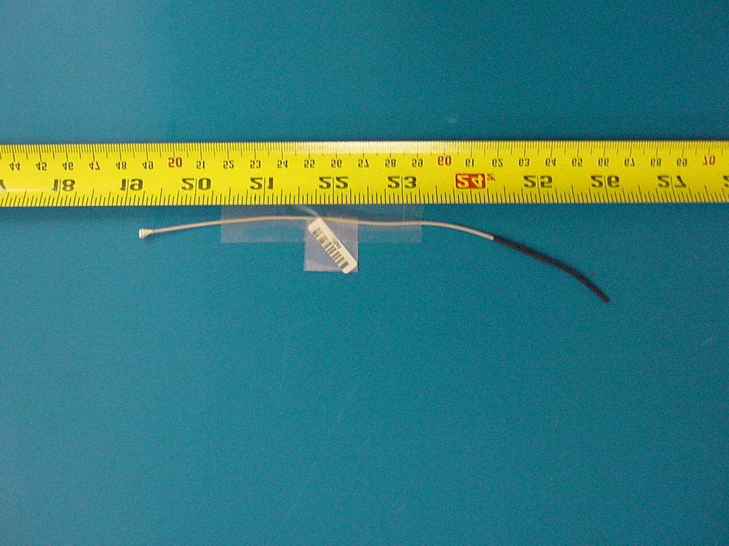
Click to zoom
Application Details
- Equipment Class
- DTS - Digital Transmission System
- Date of Grant
- Oct 25, 2001
- Application Purpose
- Original Equipment
- Date of Application
- Oct 25, 2001
- Equipment Note
- WLAN Card Inside Notebook PC
- Frequency Range
- 2410.00000000 - 2463.00000000
- Company
- Samsung Electronics Co Ltd
- Country
- United States
Documents & Files
Document Text
Text extracted from the exhibit documents filed with the FCC. Open a document above to read the original.
Users Manual
Notices i Notices No part of this publication may be reproduced, stored in a retrieval system, or transmitted, in any form or by any means, mechanical photocopying, recording or otherwise, without the prior written permission of the manufacturer. The information within this manual is subject to change without notice. The manufacturer shall not be held liable for technical or editorial errors or omissions contained in herein; nor for incidental or consequential damages resulting from the furnishing, performance or use of this material. Microsoft Windows is a registered trademark of the Microsoft Corporation. Product names mentioned herein are for identification purposes only, and may be trademarks and/or registered trademarks of their respective companies. Copyright2001 All rights are reserved ii Users Manual Important Safety Information Safety Instructions Your system is designed and tested to meet the latest standards for safety of information technology equipment. However, to ensure safe use of this product, it is important that the safety instructions marked on the product and in the documentation are followed. Always follow these instructions to help guard against personal injury and damage to your system. i Setting Up your System • Read and follow all instructions marked on the product and in the documentation before you operateyour system. Retain all safety and operating instructions for future use. • Do not use this product nearwater or a heat sourcesuch as a radiator. • Set up the system on a stable work surface. • The product should be operated only with the type of power source indicated on the rating label. • Ensure that the electrical outlet you are using to power your equipment is easily accessible in case of fire or short circuit. • If your computer has a voltage selector switch, make sure that the switch is in the proper position for your area. • Openings in the computer case are provided for ventilation. Do not block or cover these openings. Make sure you provide adequate space, at least 6 inches (15 cm), around the system for ventilation when you set up your work area. Never insert objects of any kind into the computer ventilation openings. • Ensure that the fan vents on the bottom of the casing are clear at all times. Do not place the computer on a soft surface, doing so will block the bottom vents. • The computer product is equipped with a three-wire power cord to make sure that the product is properly grounded when in use. The plug on this cord will fit only into a grounding-type outlet. This is a safety feature. If you are unable to insert the plug into an outlet, contact an electrician to install the appropriate outlet. Important Safety Information iii • If you use an extension cord with this system, make sure that the total ampere rating on the productsplugged into the extension cord does not exceed the extension cord ampere rating. Care During Use • Do not walk on the power cord or allow anything to rest on it. • Do not spill anything on the system. The best way to avoid spills is to not eat or drink near your system. • Some products have a replaceable CMOS battery on the system board. There is a danger of explosion if the CMOS battery is replaced incorrectly. Replace the battery with the same or equivalent type recommended by the manufacturer. Dispose of batteries according to the manufacturer’s instructions. If the CMOS battery requires replacement insure that a qualified technician performs the task • When the computer is turned off, a small amount of electrical current still flows through the computer. To avoid electrical shock, always unplug all power cables, remove the battery and modem cables from the wall outlets before cleaning the system. • Unplug the system from the wall outlet and refer servicing to qualified personnel if: – The power cord or plug is damaged. – Liquid has been spilled into the system. – The system does not operate properly when the operating instructions are followed. – The system was dropped or the casing is damaged. – The system performance changes. Replacement Parts and Accessories Use only replacement parts and accessories recommended by manufacturer. To reduce the risk of fire, use only No. 26 AWG or larger telecommunications line cord. Do not use this product in areas classified as hazardous. Such areas include patient care areas of medical and dental facilities, oxygen rich environments, or industrial areas. iv Users Manual Battery Disposal Do not put rechargeable batteries or products powered by non-removable rechargeable batteries in the garbage. Contact the Samsung Helpline for information on how to dispose of batteries that you cannot use or recharge any longer. Follow all local regulations when disposing of old batteries. Federal Communications Commission (FCC) v Federal Communications Commission (FCC) This device complies with Part 15 of the FCC Rules. Operation is subject to the following two conditions:(1) this device may not cause harmful interference, and (2) this device must accept any interference received, including interference that may cause undesired operation. This equipment has been tested and found to comply with the limits for a Class B digital device pursuant to Part 15 of the FCC Rules. These limits are designed to provide reasonable protection against harmful interference in a residential installation. This equipment generate uses and can radiate radio frequency energy and if not installed and used in accordance with the instructions may cause harmful interference will not occur in a particular installation. If this equipment does cause harmful interference to radio or television reception, which can be determined by turning the equipment off and on, the user is encouraged to try to correct the interference by one or more of the following measures: • Reorient or relocate the receiving antenna. • Increase the separation between the equipment and receiver. • Connect the equipment into an outlet on a circuit…
Text truncated - open the document above for the full version.
Cover Letter(s)
Page 1 of 1 https://gullfoss2.f.../TCB_Grant_Form.hts?application_id=101920&mode=COPY&fcc_id=A3LS9510/23/2001 GRANT OF EQUIPMENT AUTHORIZATION Certification Issued Under the Authority of the Federal Communications Commission By: Compliance Certification Services 561F Monterey Road Morgan Hill,CA 95037 Date of Grant: 08/06/2001 Application Dated: 08/06/2001 Samsung Electronics Co Ltd 416 Maetan-3Dong, Paldal-Ku Suwon City Kyungki-Do, Korea 441 Attention: Wallace Oh NOT TRANSFERABLE EQUIPMENT AUTHORIZATION is hereby issued to the named GRANTEE, and is VALID ONLY for the equipment identified hereon for use under the Commission's Rules and Regulations listed below. FCC IDENTIFIER A3LS950 Name of Grantee Samsung Electronics Co Ltd Equipment Class: Part 15 Class B Computing Device/Personal Computer Notes: Notebook Computer Grant Notes FCC Rule Parts Frequency Range (MHZ) Output Watts Frequency Tolerance Emission Designator 15B -
Cover Letter(s)
American Telecommunications Certification Body Inc. 6731 Whittier Ave, McLean, VA 22101 October 23, 2001 RE: Samsung Electronics FCC ID: A3LS950WL Please review my comments on this Application. 1.) Application is for a wireless LAN card located inside a notebook computer. It is unclear if the Application for Certification covers only the LAN card, or LAN card plus computer. Please enlighten. 2.) Block Diagram is for the entire computer, but excludes the LAN card. Block Diagram also does not meet the requirements of 2.1033(b)(5) 3.) Operational Description is not nearly detailed enough, and does not meet requirements of 2.1033(b)(4). Please provide a description of how device operates. 4.) Schematics supplied are for the laptop only. There are no schematics supplied for the radio board. 5.) Schematics indicate there are provisions for a Bluetooth transmitter. Please indicate how the two radios will interact and still meet the RF Exposure requirements. 6.) Test Setup does not show a complete system was tested in accordance with ANSI C63.4 requirements. Explain. 7.) Wrong language in RF Exposure Exhibit. Only 20cm distance is permitted for devices within the Mobile classification for RF Exposure. 8.) There is no language in the Manual for limiting RF Exposure. William H. Graff Examining Engineer President and Director of Engineering mailto:[email protected] The items indicated above must be submitted before processing can continue on the above referenced application. Failure to provide the requested information may result in application termination. Correspondence should be considered part of the permanent submission and may be viewed from the Internet after a Grant of Equipment Authorization is issued. Please do not respond to this correspondence using the email reply button. In order for your response to be processed expeditiously, you must submit your documents through the AmericanTCB.com website. Also, please note that partial responses increase processing time and should not be submitted. Any questions about the content of this correspondence should be directed to the sender.
Cover Letter(s)
September 22, 2000 American Telecommunications Certification Body, Inc. 6731 Whittier Avenue Suite C110 McLean, VA 22101 To Whom It May Concern: Please be advised that Samsung authorizes Rhein Tech Laboratories, Inc. to act on our behalf, until otherwise notified, for applications submitted to American Telecommunications Certification Body, Inc. (ATCB). We certify that we are not subject to denial of federal benefits, that includes FCC benefits, pursuant to Section 5301 of the Anti-Drug Abuse ACT of 1988, U.S.C. 862. Further, no party, as defined in 47 CFR 1.2002(b), to the application is subject to denial of federal benefits, that includes FCC benefits. Thank you for your attention to this matter.
External Photos
360 Herndon Parkway Suite 1400 Herndon, VA 20170 http://www.rheintech.com Certification Report Samsung Electronics Page 41 of 42 Document Number: 2001224 / QRTL01-218 FCC ID: A3LS950WT APPENDIX J: ANTENNA PHOTOGRAPHS PHOTOGRAPH 7: WLAN MICROTRIP ANTENNA 360 Herndon Parkway Suite 1400 Herndon, VA 20170 http://www.rheintech.com Certification Report Samsung Electronics Page 42 of 42 Document Number: 2001224 / QRTL01-218 FCC ID: A3LS950WT PHOTOGRAPH 8: WLAN DIPOLE ANTENNA
ID Label/Location Info
Inside this Computer is: FCC ID: A3LS950WL LABEL LOCATION
Internal Photos
360 Herndon Parkway Suite 1400 Herndon, VA 20170 http://www.rheintech.com Certification Report Samsung Electronics Page 37 of 42 Document Number: 2001224 / QRTL01-218 FCC ID: A3LS950WT APPENDIX I: INTERNAL PHOTOGRAPHS PHOTOGRAPH 3: TOP VIEW 360 Herndon Parkway Suite 1400 Herndon, VA 20170 http://www.rheintech.com Certification Report Samsung Electronics Page 38 of 42 Document Number: 2001224 / QRTL01-218 FCC ID: A3LS950WT PHOTOGRAPH 4: BOTTOM VIEW 360 Herndon Parkway Suite 1400 Herndon, VA 20170 http://www.rheintech.com Certification Report Samsung Electronics Page 39 of 42 Document Number: 2001224 / QRTL01-218 FCC ID: A3LS950WT PHOTOGRAPH 5: TOP VIEW OF THE BOARD WITHOUT CAN 360 Herndon Parkway Suite 1400 Herndon, VA 20170 http://www.rheintech.com Certification Report Samsung Electronics Page 40 of 42 Document Number: 2001224 / QRTL01-218 FCC ID: A3LS950WT PHOTOGRAPH 6: BOTTOM VIEW OF THE BOARD WITHOUT CAN
Operational Description
NEDERLAND B.V. Aug2000 DESCRIPTION ORINOCO MiniPCI Radio 2.4 GHz (World) This ORINOCO MiniPCI radio provides a (WaveLAN compatible) wireless connection for portable and mobile computers in accordance with IEEE standard 802.11 DSSS. It can work at 11, 5.5, 2 or 1 Mbps. The operation is in accordance with IEEE 802.11. The product, one piece of hardware, contains the following blocks: - MiniPCI interface - Wireless Medium Access Control (WMAC); this chip is used for handshaking with the PCI bus and for handling the IEEE protocol; it also does frequency management and interfaces to FlashROM for parameters on frequencies and Call codes. Here also selection for 11, 5.5, 2 or 1 Mbps is handled. - Digital signal processor takes care of all modulation/demodulation for DSSS for all above rates and can do selection out of 2 receiving antennae - Antenna function, provides a connection to the antennas. Optionally it can be equipped with a factory installable data encryption feature (WEP). Block Diagram MiniPCI Interface Connector The technical specification is as follows on the next page. Antenna Conn . WMAC DIGITAL SIGNAL PROCESSOR NEDERLAND B.V. May99 TECHNICAL SPECIFICATION ORINOCO MiniPCI Radio 2.4 GHz (World) Data Signalling Rate: 11, 5.5, 2 or 1 Mbit/s Media Access Protocol: According to IEEE 802.11 DSSS, CSMA/CA (Collision Avoidance) Bit Error Rate: Better than 10-8 Base-Band Modulation: - 2 Mbps: Differential Quadrature Phase Shift (before spreading) Keying (DQPSK) 2 bits/symbol - 11 and 5.5 Mbps: Complementary Code Keying Differential Quadrature Phase Shift Keying (DQPSK CCK) Spread Spectrum: Direct Sequence with 11 chips/symbol interval. Pseudo random Barker code sequence: { 1 -1 1 1 -1 1 1 1 -1 -1 -1 } Chipping Rate: 11 Mchips/s Carrier Frequency: Selectable from factory pre-programmed set according to IEEE 802.11: 2412, 2417, 2422, 2427, 2432, 2437, 2442, 2447, 2452, 2457 and 2462 MHz Peak Output Power: < 32 mW rms power (15 dBm)
RF Exposure Info
APPROVAL SHEET FOR : SAMSUNG ELECTRONICS CO., LTD MODEL : Matrix II+ Antenna DESCRIPTION : Dipole & Microstrip Antenna 0B01WMP240A1 (Microstrip antenna) SUPPLIER P/N: 0B02WDC240A1 (Dipole antenna) CUSTOMER P/N : FILE NO. : DATE : 19 July 2001 Light Tek Co., Ltd. 2 nd F , NO.158 , Gan Cheng Rd., TEL : 886-2-89510688 Pan Chiao City , Taipei Hsien , FAX : 886-2-89510681 Taiwan R.O.C . Manager Supervisor Engineer Dan Chen Lee Jackson Liu 2 1. Antenna Mechanical Dimensions : 3 2.Antenna Electrical Characteristics : 4 LIGHT TEK CO. LTD Frequency Band :2.4~2.5GHz Date :19 July 2001 Return Loss VSWR P/N : 0B01WMP240A1 5 2-1.Antenna Electrical Characteristics : LIGHT TEK CO. LTD Frequency Band :2.4~2.5GHz Date :19 July 2001 3 .Antenna Radiation Pattern : Return Loss VSWR P/N : 0B02WDC240A1 6 LIGHT TEK CO. LTD Testing Condition : Anechoic chamber P/N : 0B01WMP240A1 Date : 19 July 2001 Date : 30 Jun. 2001 Matrix II+ Micorstrip antenna LCD open Vertical X-Y plane jackson 3-1 .Antenna Radiation Pattern : 7 LIGHT TEK CO. LTD Testing Condition : Anechoic chamber P/N : 0B01WMP240A1 Date : 19 July 2001 Date : 30 Jun. 2001 Matrix II+ Micorstrip antenna LCD open Horizontal X-Y plane jackson 3-2 .Antenna Radiation Pattern : 8 LIGHT TEK CO. LTD Testing Condition : Anechoic chamber P/N : 0B01WMP240A1 Date : 19 July 2001 Microstrip antenna Date : 30 Jun. 2001 Matrix II+ LCD open Synthetic (H+V) X-Y plane Peak gain =-2.1826dBi Average gain =-7.3256dBi jackson 3-3 .Antenna Radiation Pattern : 9 LIGHT TEK CO. LTD Testing Condition : Anechoic chamber P/N : 0B01WMP240A1 Date : 19 July 2001 Date : 30 Jun. 2001 Matrix II+ Micorstrip antenna LCD closed Vertical X-Y plane jackson 3-4 .Antenna Radiation Pattern : 10 LIGHT TEK CO. LTD Testing Condition : Anechoic chamber P/N : 0B01WMP240A1 Date : 19 July 2001 Date : 30 Jun. 2001 Matrix II+ Micorstrip antenna LCD closed Horizontal X-Y plane jackson 3-5 .Antenna Radiation Pattern : 11 LIGHT TEK CO. LTD Testing Condition : Anechoic chamber P/N : 0B01WMP240A1 Date : 19 July 2001 Microstrip antenna Date : 30 Jun. 2001 Matrix II+ LCD closed Synthetic (H+V) X-Y plane Peak gain =-1.8237dBi Average gain =-6.269dBi jackson 3-6 .Antenna Radiation Pattern : 12 LIGHT TEK CO. LTD Testing Condition : Anechoic chamber P/N : 0B02WDC240A1 Date : 19 July 2001 Date : 28 Jun. 2001 Matrix II+ Dipole antenna LCD OPEN Vertical X-Y plane jackson 3-7 .Antenna Radiation Pattern : 13 LIGHT TEK CO. LTD Testing Condition : Anechoic chamber P/N : 0B02WDC240A1 Date : 19 July 2001 Date : 28 Jun. 2001 Matrix II+ Dipole antenna LCD OPEN Horizontal X-Y plane jackson 3-8 .Antenna Radiation Pattern : 14 LIGHT TEK CO. LTD Testing Condition : Anechoic chamber P/N : 0B02WDC240A1 Date : 19 July 2001 Transmitting pattern Dipole antenna Date : 28 Jun. 2001 Matrix II+ LCD open Synthetic (H+V) X-Y plane Peak gain =-1.5927dBi Average gain =-6.1867dBi jackson 3-9 .Antenna Radiation Pattern : 15 LIGHT TEK CO. LTD Testing Condition : Anechoic chamber P/N : 0B02WDC240A1 Date : 19 July 2001 Date : 28 Jun. 2001 Matrix II+ Dipole antenna LCD closed Vertical X-Y plane jackson 3-10 .Antenna Radiation Pattern : 16 LIGHT TEK CO. LTD Testing Condition : Anechoic chamber P/N : 0B02WDC240A1 Date : 19 July 2001 Date : 28 Jun. 2001 Matrix II+ Dipole antenna LCD closed Horizontal X-Y plane jackson 3-11 .Antenna Radiation Pattern : 17 LIGHT TEK CO. LTD Testing Condition : Anechoic chamber P/N : 0B02WDC240A1 Date : 19 July 2001 Transmitting pattern Dipole antenna Date : 28 Jun. 2001 Matrix II+ LCD closed Synthetic (H+V) X-Y plane Peak gain =0.5586dBi Average gain =-7.108dBi jackson 3-12 .Antenna Radiation Pattern : 18 LIGHT TEK CO. LTD Testing Condition : Anechoic chamber P/N : 0B01WMP240A1 0B02WDC240A1 Date : 19 July 2001 Receiving pattern Dipole +Microstrip antenna Date : 30 Jun. 2001 Matrix II+ LCD open Synthetic (H+V) X-Y plane jackson 3-13 .Antenna Radiation Pattern : 19 LIGHT TEK CO. LTD Testing Condition : Anechoic chamber P/N : 0B01WMP240A1 0B02WDC240A1 Date : 19 July 2001 Receiving pattern Dipole +Microstrip antenna Date : 30 Jun. 2001 Matrix II+ LCD closed Synthetic (H+V) X-Y plane jackson 20 4. SPECIFICATIONS: Electrical Properties Frequency Range............. 2.4~2.5GHz Impedance...................... 50 Ohms nominal VSWR............................ <2.0 Peak Gain....................... -5Bi < peak gain < 3dBi Standard Connector.......... HIROSE Female Connector 5. IEEE .802.11 and BLUETOOTH Antenna Testing Conditions : 21 NoteBook Placement : c 180 degree clockwise LCD OPEN LCD CLOSE 750 cm HORN Standard Antenna 8753ES Network Analyzer Rotator Controller Radiation Pattern Testing - Anechoic Chamber Center : DUT Antenna
RF Exposure Info
360 Herndon Parkway Suite 1400 Herndon, VA 20170 http://www.rheintech.com Certification Report Samsung Electronics Page 28 of 42 Document Number: 2001224 / QRTL01-218 FCC ID: A3LS950WT 9 FCC PART 1 & 2 §1.1307; 1.1310; 2.1091; 2.1093 RF EXPOSURE CALCULATIONS FOR HIGH GAIN ANTENNAS From FCC 1.1310 table 1A, the maximum permissible RF exposure for an uncontrolled environment is 1mW/cm 2. The Electric field generated for a 1mW/cm 2 exposure (S) is calculated as follows: S = E 2 /Z where: S = Power density E = Electric field Z = Impedance. E = √S x Z 1mW/cm 2 = 10 W/m 2 The impedance of free space is 337 ohms, where E and H fields are perpendicular. Thus: E = √10 x 377 = 61.4 V/m which is equivalent to 1mW/cm 2 Using the relationship between Electric field E, Power in watts P, and distance in meters d, the corresponding Antenna numeric gain G and the transmitter output power and solving for d, d = √ P eak x 30 x G E Example using the Stub Omni-directional antenna 1. The Numeric gain G of antenna with a gain specified in dB is determined by: G = Log –1 (dB gain/10) G = Log –1 0.215 = 1.64 Notice in Installation Manual: While installing and operating this transmitter and antenna combination the radio frequency exposure limit of 1mW/cm 2 may be exceeded at distances close to the antennas installed. Therefore, the user must maintain a minimum distance of 20 cm from the antenna at all time. The table below identifies the distances where the 1mW/cm 2 exposure limits may be exceeded during continuous transmission using the external antenna TABLE 9-1: RF EXPOSURE SEPARATION DISTANCE Antenna Type Gain (dBi) Gain Numeric Power Output (mW) Calculated RF Exposure Separation Distance (cm) Minimum RF Exposure Separation Distance (cm) Dipole 0.5 1.1 31.0 1.6 20 Microstrip -1.8 0.6 31.0 1.2 20
Schematics
NO ASSY NO ASSY NO ASSY NO ASSY NO ASSY NO ASSY NO ASSY NO ASSY 7 8U270 DISCLOSED, REPRODUCED, OR USED except as authorized in writing by Lucent Technologies OF NIEUWEGEIN , THE NETHERLANDS SUPSD: START:- A - power detector stub RF POWER AMPLIFIER 7 7 - to which it pertains. 2000 Lucent Technologies Corp. Lucent Technologies Nederland B.V. /WCND SCALE: O DESIGNER: ORINOCO MiniPCI-3a - DFTS: in connection with the manufacture, maintenance and use of the Lucent Technologies equipment APPD:-APPD: - - - stub Schematic C - COPYRIGHT FINISH: Thursday, July 13, 20001:15:48 pm SUPERSEDES: UNIT: NAME: - 014891 CODE: CHKR: SHEET: - Lucent Technologies Corp. It is to be treated as STRICTLY CONFIDENTIAL and is NOT TO BE The content of this document is Lucent Technologies Intellectual Property and is the property of NO ASSY - Schematic A SUPSD: NIEUWEGEIN , THE NETHERLANDS - COPYRIGHT 014891 APPD: to which it pertains. C Lucent Technologies Nederland B.V. /WCND - in connection with the manufacture, maintenance and use of the Lucent Technologies equipment - DFTS: - Lucent Technologies Corp. It is to be treated as STRICTLY CONFIDENTIAL and is NOT TO BE 6 - The content of this document is Lucent Technologies Intellectual Property and is the property of SUPERSEDES: 6-- - CODE: FINISH: 7 DESIGNER:START: PCB band pass filter 8U270 IF RF CONVERTER SCALE: OF O APPD: 2000 Lucent Technologies Corp. UNIT: PCB band pass filter SHEET: ORINOCO MiniPCI-3a DISCLOSED, REPRODUCED, OR USED except as authorized in writing by Lucent Technologies NAME: - - CHKR: VDDCP 13 16 XTAL1 15 XTAL2 GNDCP 1 LOCK 11 PHA PHI 98 PHP 20 PON 5 RFIN+ 6 RFIN- 14 RSET 2 TEST VDD 3 SA8026 U206 12 AUXin CLK 1718 DATA 19 E_ 4 GND GND2 10 7 - 014891 4 Lucent Technologies Corp. It is to be treated as STRICTLY CONFIDENTIAL and is NOT TO BE START: to which it pertains.FINISH: DFTS: NIEUWEGEIN , THE NETHERLANDS 2 C - 3 OF 6 NAME: DISCLOSED, REPRODUCED, OR USED except as authorized in writing by Lucent Technologies 4 - Lucent Technologies Nederland B.V. /WCND SCALE: A 5 E - 6 R in connection with the manufacture, maintenance and use of the Lucent Technologies equipment 8U270 D E - D - 2000 Lucent Technologies Corp. 5 A - DESIGNER: APPD: C F APPD: 7 B SHEET: CHKR:COPYRIGHT CODE: 2 The content of this document is Lucent Technologies Intellectual Property and is the property of 1 IF TRANCEIVERSchematic A O SUPSD: - 7 - - ORINOC MiniPCI-3a V - 1 B 8 Thursday, July 13, 2000 1:10:54 pm C UNIT: 7 5 3 5 E 8 F SUPERSEDES: NO ASSY NO ASSY 2000 Lucent Technologies Corp. 8U270 C E OF BE CODE: 5 44 Lucent Technologies Corp. It is to be treated as STRICTLY CONFIDENTIAL and is NOT TO BE SHEET: R 7 D - 7 - CHKR: 8 Lucent Technologies Nederland B.V. /WCND COPYRIGHT 6 - O B DISCLOSED, REPRODUCED, OR USED except as authorized in writing by Lucent Technologies NAME: DFTS: A ORINOCO MiniPCI-3a - 7 START: 1 3 - The content of this document is Lucent Technologies Intellectual Property and is the property of SUPSD: 014891 APPD: 4 F 2 E 3 SCALE: - 6 Thursday, July 20, 2000 12:58:27 pm 2 A 8 C 4 in connection with the manufacture, maintenance and use of the Lucent Technologies equipmentto which it pertains. - 5 - D V SUPERSEDES: 1 F Schematic UNIT: HERMES AND THESEUS APPD: A - - DESIGNER: NIEUWEGEIN , THE NETHERLANDS - FINISH: C NO ASSY NO ASSYNO ASSY NO ASSY ORINOCO MiniPCI-3a - START:APPD: CODE: 7 2 5 8 A 3 4 O 3 B 1 E Schematic 7 C 8 C POWER SUPPLY - SHEET: 3 DESIGNER: - 6 A 1 F 6 R - V - 4 CHKR: - to which it pertains. DFTS: 5 APPD: C - UNIT: 3 SUPSD: in connection with the manufacture, maintenance and use of the Lucent Technologies equipment 8U270 2000 Lucent Technologies Corp. - 014891 E NAME: Lucent Technologies Corp. It is to be treated as STRICTLY CONFIDENTIAL and is NOT TO BE SCALE: - - 2.85V 2.85V DISCLOSED, REPRODUCED, OR USED except as authorized in writing by Lucent Technologies D A - SUPERSEDES: OF FINISH: NIEUWEGEIN , THE NETHERLANDS The content of this document is Lucent Technologies Intellectual Property and is the property of Lucent Technologies Nederland B.V. /WCND 7 F B D E COPYRIGHT 2 Thursday, July 13, 2000 1:08:56 pm NO ASSY NO_ASSY NO ASSY NO ASSY NO ASSY NO ASSY NO ASSY NO ASSY SUPSD: D 1 R Lucent Technologies Corp. It is to be treated as STRICTLY CONFIDENTIAL and is NOT TO BE 2 8U270 - CHKR: 6 DESIGNER: E APPD: 8 D V APPD: C 5 E 3 SCALE: B DFTS: 1 7 FINISH: - 2 - in connection with the manufacture, maintenance and use of the Lucent Technologies equipment NIEUWEGEIN , THE NETHERLANDS ORINOCO MiniPCI-3a 3 - UNIT: C - A Lucent Technologies Nederland B.V./WCND - 4 - The content of this document is Lucent Technologies Intellectual Property and is the property of 4 SHEET: B - START: OF 2 MINI PCI CON CODE: 5 DISCLOSED, REPRODUCED, OR USED except as authorized in writing by Lucent TechnologiesCOPYRIGHT 7 A 6 F F E was GND - SUPERSEDES: 8 C - EDGE CONNECTOR to which it pertains. 7 Schematic O - NAME: 2000 Lucent Technologies Corp. A 014891 2
Test Report
Engineering and Testing for EMC and Safety Compliance 360 Herndon Parkway, Suite 1400 Herndon, VA 20170 Phone: 703-689-0368; Fax: 703-689-2056; Metro: 703-471-6441 APPLICATION FOR FCC CERTIFICATION DIRECT SEQUENCE SPREAD SPECTRUM TRANSMITTER Samsung Electronics 416, Maetan-3Dong,Paldal-Gu Suwon City, Kyunggi-Do, Korea, 442-743 +82-31-200-7925 Model: Wireless LAN Card (Sens 950) FCC ID: A3LS950WT Canada: 649104504A3 17 August 20, 2001 S TANDARDS R EFERENCED FOR THIS R EPORT P ART 2: 1999 F REQUENCY A LLOCATIONS AND R ADIO T REATY M ATTERS ; G ENERAL R ULES AND R EGULATIONS P ART 15: 1999 R ADIO F REQUENCY D EVICES FCC 97-114 G UIDANCE ON M EASUREMENTS FOR D IRECT S EQUENCE S PREAD S PECTRUM S YSTEMS ANSI C63.4-1992 S TANDARD F ORMAT M EASUREMENT /T ECHNICAL R EPORT P ERSONAL C OMPUTER AND P ERIPHERALS RSS-210; I SSUE 5 (D RAFT 3) L OW P OWER L ICENCE -E XEMPT R ADIOCOMMUNICATION D EVICES (A LL F REQUENCY B ANDS RSS-102; I SSUE 1 (P ROVISIONAL ) E VALUATION P ROCEDURE FOR M OBILE AND P ORTABLE R ADIO T RANSMITTERS WITH RESPECT TO H EALTH C ANADA ’ S S AFETY C ODE 6 FOR E XPOSURE OF H UMANS TO R ADIO F REQUENCY F IELDS Frequency Range Conducted Output Power (W) Freq. Tolerance Emission Designator 2410 to 2463 MHz 0.031 REPORT PREPARED BY: EMC Engineer: Rachid Sehb Supervising Engineer: Bruno Clavier Document Number: 2001224 / QRTL01-218 No part of this report may be reproduced without the full written approval of Rhein Tech Laboratories, Inc. 360 Herndon Parkway Suite 1400 Herndon, VA 20170 http://www.rheintech.com Certification Report Samsung Electronics Page 2 of 42 Document Number: 2001224 / QRTL01-218 FCC ID: A3LS950WT TABLE OF CONTENTS 1 INTRODUCTION ......................................................................................................................................................................................4 1.1 RELATED SUBMITTAL (S)/GRANT (S) .......................................................................................................................................................................4 1.2 TEST METHODOLOGY .................................................................................................................................................................................................4 1.3 TEST FACILITY..............................................................................................................................................................................................................4 2 SYSTEM TEST CONFIGURATION .........................................................................................................................................................5 2.1 JUSTIFICATION.............................................................................................................................................................................................................5 2.2 EUT EXERCISE SOFTWARE........................................................................................................................................................................................5 2.3 SPECIAL ACCESSORIES .............................................................................................................................................................................................5 2.4 TEST SYSTEM DETAILS ..............................................................................................................................................................................................5 2.5 CONFIGURATION OF TESTED SYSTEM8 ..................................................................................................................................................................6 3 CONFORMANCE STATEMENT..............................................................................................................................................................7 4 FIELD STRENGTH CALCULATION .......................................................................................................................................................8 5 FCC PART 15 §15.109 RADIATED EMISSIONS MEASUREMENTS....................................................................................................9 5.1 FCC PART 15 §15.109 RADIATED EMISSIONS TEST .............................................................................................................................................10 5.1.1 FCC PART 15 §15.109 RADIATED EMISSION DIGITAL NOISE......................................................................................................................................10 6 FCC PART 15 §15.247(B) POWER OUTPUT.......................................................................................................................................11 7 FCC PART 15 §15.209(C) RADIATED SPURIOUS EMISSIONS.........................................................................................................12 7.1 RADIATED EMISSIONS HARMONICS/SPURIOUS FOR THE DIPOLE ANTENNA ................................................................................................12 7.2 RADIATED EMISSIONS HARMONICS/SPURIOUS FOR THE MICROSTRIP ANTENNA .......................................................................................15 8 FCC PART 15 §15.205 COMPLIANCE WITH THE RESTRICTED BAND EDGE.…
Text truncated - open the document above for the full version.
Contact Information
Applicant
Jenni Chun(General Manager)
Technical Contact
Rhein Tech LaboratoriesRachid Sehb
[email protected]703 689 0368
360 Herndon Parkway · Herndon, Virginia · United States
Test Firm
Rhein Tech Laboratories, Inc.Rick McMurray
Technical Specifications
| # | Rule Parts | Frequency Range | Power Output |
|---|---|---|---|
| 1 | 15C | 2.41 GHz - 2.46 GHz | 31.00 mW |
Other Applications from Samsung Electronics Co Ltd
A3LSMS741B
Aug 05, 2026Portable Handset
Equipment Class
6VL - 15E 6 GHZ Very Low Power DeviceA3LSMX940
Jul 31, 2026BT,BLE Tablet DTS,UNII a,b,g,n,ac,ax,be and digitizer
Equipment Class
DTS - Digital Transmission SystemA3LSMS741U
Jul 30, 2026Portable Handset
Equipment Class
6CD - 15E 6 GHz Low Power Dual ClientA3LSMX840
Jul 27, 2026BT,BLE Tablet DTS,UNII a,b,g,n,ac,ax and Digitizer
Equipment Class
DSS - Part 15 Spread Spectrum TransmitterA3LSMX848U
Jul 27, 2026WCDMA, LTE, 5G NR Tablet BT,BLE, DTS,UNII a b g n ac ax and Digitizer
Equipment Class
JBP - Part 15 Class B Computing Device Peripheral