A3LSCWR500CELLULAR CDMA WLL TERMINAL
Samsung Electronics Co Ltd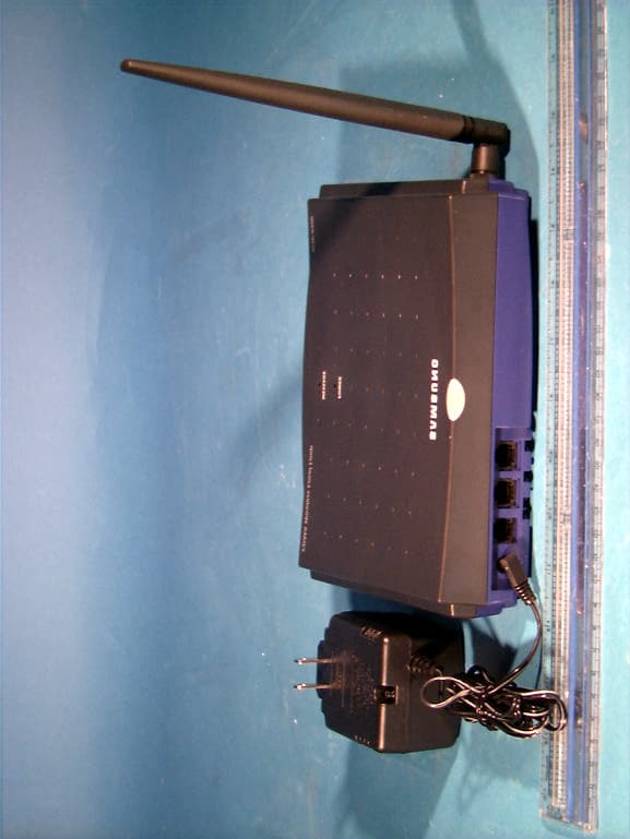
Click to zoom
Application Details
- Equipment Class
- TNB - Licensed Non-Broadcast Station Transmitter
- Date of Grant
- May 03, 1999
- Application Purpose
- Original Equipment
- Date of Application
- Feb 21, 1999
- Equipment Note
- CELLULAR CDMA WLL TERMINAL
- Frequency Range
- 824.64000000 - 848.37000000
- Company
- Samsung Electronics Co Ltd
- Country
- United States
Documents & Files
Document Text
Text extracted from the exhibit documents filed with the FCC. Open a document above to read the original.
Users Manual
ELECTRONICS Printed in KoreaCode No.: GH68-00237A’99/1 Rev 1 0(ENG) USER’S MANUAL CDMAW IRELESS L OCAL L OOP TELEPHONE SCW-R500/510 CDMAW IRELESS L OCAL L OOP TELEPHONE SCW-R500/510 SCW-R500 1/9/99 12:06 PM Page b Safety Precautions–––––––––––––––––––––––––––––2FCC NOTE ––––––––––––––––––––––––––––––––––––3Checking Parts ––––––––––––––––––––––––––––––––4Terminal Information –––––––––––––––––––––––––––5Setting Up Your Terminal –––––––––––––––––––––––6Basic Operation Making Calls –––––––––––––––––––––––––––––12Receiving Calls –––––––––––––––––––––––––––12 Advanced Features Adjusting Volume –––––––––––––––––––––––––14Terminal Reset –––––––––––––––––––––––––––14Restricting use of the phone –––––––––––––––––15Setting Warning Beeps–––––––––––––––––––––15Changing the Lock Code ––––––––––––––––––––16 Optional Features Call Waiting –––––––––––––––––––––––––––––18Three-Way Calling ––––––––––––––––––––––––18Call Forwarding–––––––––––––––––––––––––––18Caller ID ––––––––––––––––––––––––––––––––18Voice Mail Service ––––––––––––––––––––––––18 Miscellaneous Menu Options Table –––––––––––––––––––––––20Troubleshooting ––––––––––––––––––––––––––22Specifications ––––––––––––––––––––––––––––23 TABLE OF CONTENTS FEATURES DescriptionThe Fixed Wireless Terminal(FWT)s are next generationtelecommunication terminals that provide the economic efficiency ofwireless and integrated service of wireline.Samsung SCW-R500 & SCW-R510 terminals connect traditional wiredtelephones to a wireless base station which delivers the call to the publictelephone network, instead of direct wired connection the network.Due to its wireless characters : the user can easily install the terminal andcan relocate it anywhere within the serviced local area. It is especially veryconvenient to use in areas where the wired telephone installation isdifficult. The terminals will offer you with such clear digital voice quality andvarious network service features that you will not know the difference witha conventional telephone.The terminal was designed to either be used on a desk or attached to thewall. 1 Incoming Call Light 2 Received SignalStrength Indicator 3 Adjusting Volume 4 External PowerSupply(optional) SCW-R500 1/9/99 12:06 PM Page d FCC NOTE SAFETY PRECAUTIONS 1 Avoid places where there are dust, gas or fire. 2 Do not shake, hit or impact the phone. 3 If you wish to cleanse the outside of the terminal, use only a soft,dry cloth. Such chemicals as alcohol, benzine or acetone can dam-age the surface of the terminal. 4 Do not twist or pull the cord out of the terminal. 5 Do not disassemble the FWT as you please. 6 DO NOT use the power adaptor if:• The power cord is damaged.• The terminal has been dropped or damaged in any way. 7 Use only the SAMSUNG provided adaptor. Do not use the SAMSUNG adaptor for any other usage. 8 Use only the SAMSUNG provided antenna. Do not use the antennafor any other usage. 9 Do not install the terminal near water, for example, near a bath tub,sink, wet basement, or swimming pool. 10 Do not allow children to play with any radio equipment containing a transmitter. Children could hurt themselves or others (by poking themselves or others in the eye with the antenna. for example). Children could also damage the FWT. NOTE : The input voltage and the shape of the plug on this terminalmay vary from country to country. This device complies with part 15 of the FCC rules.Operation is subject to the following two conditions:1) The device may not cause harmful interference.2) This device must accept any interference received, including interference that may cause undesiredoperation. Privacy of communication may not beensured when using this phone. SCW-R500 1/9/99 12:06 PM Page 2 Once you have unpacked your consumer package, check to make sure thatyou have all the parts shown below. If any piece is missing or broken, please call your dealer. FWT Terminal Antenna AC Adaptor User's Manual, Quick Reference Card Wall Mountable Bracket External Power Supply(Optional) Wall Mounting Screws and Caps TERMINAL INFORMATION Antenna Antenna Connector RJ-11 Phone Port PowerConnector CHECKING PARTS 1 4 2 5 3 6 1 4 2 5 3 6 Wall Mountable Bracket.Wall Mounting Screws and Caps Option Voice mail LED RSSI LED ANTConnector Power LED RS-232C Connector SCW-R500/510 Quick Reference Card ELECTRON USER’S MANUAL CDMAW IRELESS L OCAL L OOP TELEPHONE SCW-R500/510 CDMAW IRELESS L OCAL L OOP TELEPHONE SCW-R500/510 ELECTRO ELECTRON SCW-R500 1/9/99 12:06 PM Page 4 This FWT SCW-R500/R510 operates by receiving electricity from an electricaloutlet or external power supply.1 Connect the terminal mounted Antenna on the side of the terminal. 2 Connect a conventional wired telephone to a RJ-11 phone port.(SCW-R500: 3 RJ-11 phone ports / SCW-R510: 2 RJ-11 phone port)Use the telephone compatible to FCC part 68 as possible, otherwise it may not work properly. FWT works only tone dialing. 3 Plug the AC adaptor output into the rear DC 9V jack of the Terminal. 4 Plug the AC adaptor plug into an appropriate electrical outlet. 5 Connect a G3 analog facsimile machine to a dedicated RJ-11 port.(only for SCW-R510)0 The usage of RS-232C connector on the base of the FWT is not user but dealer's maintenance. How to install External Power Supply(option) 1 Connect the DC power cable to External power supply. 2 Connect the DC power cable to FWT. 3 Connect the AC power connector to External power supply. 4 Plug the AC power connector to wall outlet. 5 Connect a wired telephone to a RJ-11 phone port Setting up your terminal SETTING UP YOUR TERMINAL 1 2 4 5 3 1 2 4 5 3 SCW-R500 1/9/99 12:06 PM Page 6 Screws and Caps are provided for mounting the unit on a wall.Screws and Caps are recommended for most wall surface.For wooden wall installations, only the screws are required.1 Mark four mounting hole locations on the wall. 2 Drill four holes at the marked location. 3 If not using Caps, drill four holes in the wood. If using Caps, drill four holes at the marked location.Insert the Caps int…
Text truncated - open the document above for the full version.
Cover Letter(s)
February 22, 1999 Federal Communications Commission Equipment Approval Services 7435 Oakland Mills Road Columbia, MD 21046 SUBJECT:SAMSUNG Electronics Co., Ltd. FCC ID: A3LSCWR500 Part 22 Certification Gentlemen: Attached herewith, on behalf of SAMSUNG Electronics Co., Ltd., is an application for Part 22 Certification of the following Cellular CDMA WLLTerminal: FCC ID:A3LSCWR500 TRADE / MODEL(s):SAMSUNG SCW-R500 EUT TYPE:Cellular CDMA WLL Terminal Tx Freq. Range:824.64 – 848.37 MHz Max. Output Power:0.22 Watts (ERP) Attached is the Letter of Authorization, Confidentiality Request, ESN affidavit, measurement report data and plots, FCC ID label and location, test setup photographs, internal and external photographs, block diagram (confidential), schematic diagrams & circuit description (confidential), operational description, parts list & tune-up procedure, and the user's manual. Should you have any questions or comments concerning the above, please contact the undersigned. cc:Mr. Ben Kim, Engineering Manager American QA Lab SAMSUNG Electronics America
Cover Letter(s)
Feb 08, 1999 Federal Communications Commission Authorization and Evaluation Division Equipment Authorization Branch 7435 Oakland Mills Road Columbia, MD 21046 In re: Samsung Electronics Co., Ltd. FCC ID.: A3LSCWR500 Wireless Local Loop Phone - Certification Request for Confidentiality To whom it may concern: In accordance with 0.459 of CFR 47, Samsung Electronics Co., Ltd. requests confidentiality for the Block Diagram, Schematics, & Circuit Description of the attached test report. These documents contains detailed system and equipment description and related information about the product which Samsung Electronics Co., Ltd. considers to be proprietary, confidential, and a custom design and otherwise, would not release to the general public. Since this design is a basis from which future technological products will evolve, Samsung feels that this information would be of benefit to its competitors, and that the disclosure of the information in these documents would give our competitors an unfair advantage in the market. Sincerely, Ben Kim Engineering Manager
External Photos
Test Report S/N: 22.990121045.A3LFCC Part 22 Test Date(s): February 08-10, 1999Certfication © 1998 PCTEST LabFCC ID: A3LSCWR500 NVLAP Lab Code: 100431-0 SAMSUNG Electronics Co., Ltd. Test Report S/N: 22.990121045.A3LFCC Part 22 Test Date(s): February 08-10, 1999Certfication © 1998 PCTEST LabFCC ID: A3LSCWR500 NVLAP Lab Code: 100431-0 SAMSUNG Electronics Co., Ltd. Test Report S/N: 22.990121045.A3LFCC Part 22 Test Date(s): February 08-10, 1999Certfication © 1998 PCTEST LabFCC ID: A3LSCWR500 NVLAP Lab Code: 100431-0 SAMSUNG Electronics Co., Ltd.
ID Label/Location Info
© 1999 PCTEST Lab FCC ID SAMPLE LABEL & LOCATION LABELLING REQUIREMENTS PER §§ 2.925 The Label shown shall be permanently affixed at a conspicuous location on the device and be readily visible to the user at the time of purchase. Fig 12. Sample label (SEE NEXT PAGE)
Internal Photos
Test Report S/N: 22.990121045.A3LFCC Part 22 Test Date(s): February 08-10, 1999Certfication © 1998 PCTEST LabFCC ID: A3LSCWR500 NVLAP Lab Code: 100431-0 SAMSUNG Electronics Co., Ltd. Test Report S/N: 22.990121045.A3LFCC Part 22 Test Date(s): February 08-10, 1999Certfication © 1998 PCTEST LabFCC ID: A3LSCWR500 NVLAP Lab Code: 100431-0 SAMSUNG Electronics Co., Ltd. Test Report S/N: 22.990121045.A3LFCC Part 22 Test Date(s): February 08-10, 1999Certfication © 1998 PCTEST LabFCC ID: A3LSCWR500 NVLAP Lab Code: 100431-0 SAMSUNG Electronics Co., Ltd. Test Report S/N: 22.990121045.A3LFCC Part 22 Test Date(s): February 08-10, 1999Certfication © 1998 PCTEST LabFCC ID: A3LSCWR500 NVLAP Lab Code: 100431-0 SAMSUNG Electronics Co., Ltd.
Operational Description
SamsungElectronics 1.Specification 1-1.General ItemSpecification FrequencyRange Tranasmitter Receiver 824.64~848.37MHz 869.64~893.37MHz ChannelBandwidthCDMA1.23MHz ChannelSpacing30kHz NumberofChannels20FA DuplexSeparation45MHz TypeofEmissionG7W Input/OutputImpedance50ohms IntermediateFrequency Transmitter Receiver 130.38MHz 210.38MHz LocalFrequency Transmitter Receiver 1st(F TX -130.38),2nd(260.76MHz) 1st(F RX -210.38),2nd(420.76MHz) TCXOFrequency19.68MHz FrequencyStability(F RX -80MHz) °æ 150Hz OperatingTemperature-20 °... ~+50 °... SupplyVoltage9VDCnorminal CurrentConsumption(Average) Standby Talk 100mA(Non-slotmode) 470mA(at+10dBm) SizeandWeight200 °ø 170 °ø 48.5mm/1000g SamsungElectronics 1-2.Transmitt er ItemSpec ifica tion WaveformQuality0.944ormore OpenLoopPowerControlRange -25dBm -65dBm -104dBm -57.5dBm~-38.5dBm -17.5dBm~+1.5dBm +18.0dBm~+30.0dBm MinimumTxPowerControl-50dBmbelow ClosedLoopPowerControlRange Test1 beyond °æ 24dB Test2 1ms~2.5ms Test3 beyond °æ 24dB Test4 beyond °æ 24dB Test5 beyond °æ 24dB MaximumRFOutputPower220mW(+23.4dBm) OccupiedBandwidth1.23MHz [email protected]/30kHz 1-3.Receiver ItemSpec ifica tion RxSensitivityandDynamicRange (RateSet1) -104dBm,FER=0.5%orless -25dBm,FER=0.5%orless ConductedSpuriousEmission 869~894MHz 824~849MHz AllOtherFrequency below-81dBm/1MHz below-61dBm/1MHz below-47dBm/30kHz SingleToneDesensitization Rxpower=-101dBm Tonepower=-30dBm Toneoffsetfromcarrier= °æ 900kHz FER=lowerthan1% SamsungElectronics IntermodulationSpuriousResponseAttenuation Rxpower=-101dBm Tonepower1=-43dBm Tonepower2=-43dBm Tone1offsetfromcarrier= °æ 900kHz Tone2offsetfromcarrier= °æ 1700kHz Rxpower=-90dBm Tonepower1=-32dBm Tonepower2=-32dBm Tone1offsetfromcarrier= °æ 900kHz Tone2offsetfromcarrier= °æ 1700kHz Rxpower=-79dBm Tonepower1=-21dBm Tonepower2=-21dBm Tone1offsetfromcarrier= °æ 900kHz Tone2offsetfromcarrier= °æ 1700kHz FER=lowerthan1% 1-4.Antenna ItemSpecification Frequency824~894MHz Gain2 °æ 1.0dBi VSWRlessthan1.9:1 Impedance50ohms Size210.7 °æ 1.5mm Temperature-30 °... ~+60 °... InputconnectorBNC-Male SamsungElectronics 1-5.Channelvs.FrequencyTable FANo.CHNo.TX[MHz]RX[MHz] 11011824.64869.64 229825.87870.87 370827.10872.10 4111828.33873.33 5152829.56874.56 6193830.79875.79 7234832.02877.02 8275833.25878.25 9316834.48879.48 10363835.89880.89 11404837.12882.12 12445838.35883.35 13486839.58884.58 14527840.81885.81 15568842.04887.04 16609843.27888.27 17650844.50889.50 18697845.91890.91 19738847.14892.14 20779848.37893.37
Parts List/Tune Up Info
SamsungElectronics 1-1.Introduction The'AutotestProgram'isthetestprogramforSCW-R500in'testmode'.Youshouldrunthe 'AutotestProgram'inyourPCornotebooktocontrolSCW-R500intestmode. 1-2.ListofEquipment °§ DUT(DeviceUnderTest);SCW-R500 °§ RFCable °§ RS232CCable °§ Adaptor(9VDC/1.2A) °§ PC(IBMorcompatiblecomputer);atleast80386-SX °§ SpectrumAnalyzer;HP8596E 1-3.ConfigurationofTest WhenyoucheckDUTworksrightly,youmayconnectSpectrumAnalyzer. Adaptor 9V/1.2A PCControl TestBoard RS232CCable SpectrumAnalyzer Antenna SamsungElectronics 1-4.TestProcedure 1-4-1. Start in Normal Mode 1.WhenyouconnectaDUT(SCW-R500)withtheadaptor,youcanseethe'power'LEDis ON(red)ontheDUT.Inafewminuteslater,theDUTentersinto'NormalMode'inthestate ofwhichyoucanmakeacallwithCDMAMobileStationTestSet(HP8924C,CMD-80etc.). 1-4-2. Change to Test Mode 1.ConnectDUTtoPCwithRS232Cserialinterfacecable. 2.Runthe'AutotestProgram'inyourPC. If"F1:SCW-R5000"ischosenwithstart, choose "F2 : SCW-R500" by pushing F2 key. Therearetwowaysofselectingthetestcommandyouwant;oneisapull-downtypein whichyoucanselectthetestcommandbymoving" °Ë "and" °È "keysandhittingtheenter key,theotheriswritingthetestcommandnumberin"inputcommand"sectiondirectlyand hittingtheenterkey. 3.YoucanchangeDUTfromNormalModeintoTestModewhenyouenterthecommand"00" (EntertoTestMode).Ifrightlyinitialized,"ACKed"messageandsomenumbersatTerminal Info.(S/W,ESN,NAM)sectionwilldisplay. 4.Thecommand"01"(Suspend)isenteredtostartthetest. 5.TofinishorrestarttheTestMode,youshouldenterthecommand"02".Andifyouwantto exittheAutotestProgram,hitthe"escapekey"inthekeyboard. 1-4-3. Carrier ON/OFF and Spreading Signal 1.Thecommand"07"(TurnonCarrier)turnsthecarrieron. 2.Ifyouwanttoturnoffthecarrier,enterthecommand"08"(TrunoffCarrier). 3.Thecommand"34"(CDATA)spreadsthesignalintoCDMAspectrum. 1-4-4. Tx Power Output level Control 1.Ifyouenterthecommand"71"(SetCDMATxAGC),youcancontroltheTxpoweroutput levelbywritinganAGCcode.TheAGCcoderangeis000~511code. NotetheAGCcodemustbewrittenin3-digit.Forexample,ifyouwant5,43,300AGC code,youmustwrite °∏ 005 °π , °∏ 043 °π and °∏ 300 °π respectively. SamsungElectronics 2.YoucanconfirmtheAGCcodeyousetinDUTbyenteringthecommand"71"andjust hitting"enterkey"oncemorewithoutwritinganAGCcode. 3.The AGC codes for Tx. max power(23dBm) and radiated spurious test power(-13dBm) are presented in 1-5. 1-4-5. Channel Selection 1.Ifyouenterthecommand"09"(Setchannel),youcanselectthechannel.Similarlytoentering anAGCcode,thechannelnumbermustbewrittenin4-digit.Forexample,ifyouwant 1011,363and779channel,youmustwrite °∏ 1011 °π , °∏ 0363 °π and °∏ 0779 °π respectively. 2.YoucanconfirmthechannelyousetinDUTbyenteringthecommand"09"andjusthitting "enterkey"oncemorewithoutwritingachannelnumber. 1-4-6. RS232C Port Test 1.Thecommand"32"(RS232CPortTest)makestheDUTcommunicatewiththeconnectedPC. 2.Writeanarbitraty6-digitnumericalvalueandhitthe"enterkey".Youwillfindthe6-digit numericalvalueyouwroteshiftstotheleftby1-digitinevery500msecifrightlyperformed. 1-5.AGCcodeforspecificTxoutputpowers Channel OutputPwr. CH1011CH363CH779 -13dBm290290293 23dBm450446466
Test Report
© 1999 PCTEST Engineering Lab., Inc. PCTEST Engineering Laboratory, Inc. 6660-B 6660-B DobbinDobbin Road Road •• Columbia, MD 21045 Columbia, MD 21045 •• U.S.A. U.S.A. TEL (410) 290-6652 TEL (410) 290-6652 •• FAX (410) 290-6654 FAX (410) 290-6654 http://www.pctestlab.comhttp://www.pctestlab.com CERTIFICATE OF COMPLIANCE (Part 22 Certification) Samsung Electronics Co., Ltd.Dates of Tests: February 08-10, 1999 146 Maetun-3 Dong, Paldal-KuTest Report S/N: 22.990121045.A3L Suwon City, Kyungki-Do, KOREA 441-742Test Site: PCTEST Lab, Columbia MD Attention: Ben Kim, Engineering Manager American QA Lab FCC ID A3LSCWR500 APPLICANT SAMSUNG ELECTRONICS CO., LTD. Classification:Non-Broadcast Station Transmitter (TNB) FCC Rule Part(s):§§§§22(H), 2.983, 2.987 EUT Type:Cellular CDMA WLL Terminal Trade Name/Model(s):SAMSUNG SCW-R500 Tx Frequency Range:824.64 ~ 848.37 MHz Rx Frequency Range:869.64 ~ 893.37 MHz Max Output Power:0.22 W (ERP) Frequency Tolerance:0.00025% (2.5 ppm) This equipment has been shown to be capable of compliance with the applicable technical standards as indicated in the measurement report and was tested in accordance with the measurement procedures specified in §2.947 with the following remarks (Note Codes): * (BC) The output power is continuously variable from the value listed in this entry to 5%-10% of the value listed. attest to the accuracy of data. All measurements reported herein were performed by me or were made under my supervision and are correct to the best of my knowledge and belief. I assume full responsibility for the completeness of these measurements and vouch for the qualifications of all persons taking them. PCTEST certifies that no party to this application has been denied the FCC benefits pursuant to Section 5301 of the Anti-Drug Abuse Act of 1988, 21 U.S.C. 853(a) 990121045.A3L FCC Part 22Certification © 1999 PCTEST Engineering Laboratory, Inc.FCC Part 22 TABLE OF CONTENTS ATTACHMENT A: COVER LETTER(S) ATTACHMENT B: ATTESTATION STATEMENT(S) ATTACHMENT C: TEST REPORT SCOPE 1 INTRODUCTION 2 DESCRIPTION OF TESTS 3-6 EFFECTIVE RADIATED POWER OUTPUT 7 RADIATED MEASUREMENTS 8-10 FREQUENCY STABILITY 11-12 PLOTS OF EMISSIONS 13 LIST OF TEST EQUIPMENT 14 SAMPLE CALCULATIONS 15 RECOMMENDATION / CONCLUSION 16 ATTACHMENT D: TEST PLOTS ATTACHMENT E: FCC ID LABEL / LOCATION ATTACHMENT F: TEST SETUP PHOTOGRAPHS ATTACHMENT G: EXTERNAL PHOTOGRAPHS ATTACHMENT H: INTERNAL PHOTOGRAPHS ATTACHMENT I: BLOCK DIAGRAM(S) ATTACHMENT J: SCHEMATIC DIAGRAM(S) ATTACHMENT K: PARTS LIST/TUNE UP PROCEDURE ATTACHMENT L:OPERATIONAL DESCRIPTION ATTACHMENT M:USER’S MANUAL Test Report S/N: 22.990121045.A3LFCC Part 22 Test Dates: February 08-10, 1999Certification © 1999 PCTEST LabSAMSUNG FCC ID: A3LSCWR500 (Tx 824-849MHz)1 Cellular CDMA WLL Terminal (Model: SCW-R500) MEASUREMENT REPORT Scope - Measurement and determination of electromagnetic emissions (EME) of radio frequency devices including intentional and/or unintentional radiators for compliance with the technical rules and regulations of the Federal Communications Commission. §2983(a) General Information Applicant Name:SAMSUNG ELECTRONICS CO., LTD. Address:146 Maetun-3 Dong, Paldal-Ku Suwon City, Kyungki-Do, KOREA 441-742 Attention:Ben Kim, Engineering Manager American QA Lab • §2983(b) FCC ID:A3LSCWR500 • Trade Name:SAMSUNG • Model(s):SCW-R500 • §2983(c) Quantity:Quantity production is planned • §2.983(d) Emission Designator:1M25F9W • §2.983(d) Tx Freq. Range:824.64 – 848.37 MHz Rx Freq. Range:869.64 – 893.37 MHz • Equipment Class:Non-Broadcast Station Transmitter (TNB) • Equipment Type:Cellular CDMA WLL Terminal • Modulation:CDMA • Frequency Tolerance:± 0.00025% (2.5 ppm) • §2.983(d) Max. Power:0.22 W (ERP) • FCC Rule Part(s):§§§§ 22(H), 2.983, 2.987 • AC/DC Charger:120 VAC SAMSUNG Model: F5000ADP • Dates of Tests:February 08-10, 1999 • Place of Tests:PCTEST Lab, Columbia, MD U.S.A. • Test Report S/N:22.990121045.A3L Test Report S/N: 22.990121045.A3LFCC Part 22 Test Dates: February 08-10, 1999Certification © 1999 PCTEST LabSAMSUNG FCC ID: A3LSCWR500 (Tx 824-849MHz)2 Cellular CDMA WLL Terminal (Model: SCW-R500) 1.1 INTRODUCTION These measurement tests were conducted at PCTEST Engineering Laboratory, Inc. facility in New Concept Business Park, Guilford Industrial Park, Columbia, Maryland. The site address is 6660-B Dobbin Road, Columbia, MD 21045. The test site is one of the highest points in the Columbia area with an elevation of 390 feet above mean sea level. The site coordinates are 39° 11'15" N latitude and 76° 49'38" W longitude. The facility is 1.5 miles North of the FCC laboratory, and the ambient signal and ambient signal strength are approximately equal to those of the FCC laboratory. There are no FM or TV transmitters within 15 miles of the site. The detailed description of the measurement facility was found to be in compliance with the requirements of § 2.948 according to ANSI C63.4 on October 19, 1992. Measurement Procedure The radiated and spurious measurements were made outdoors at 3-meter test range (see Figure2). The equipment under test is placed on the turntable connected to a RF wattmeter and a dummy RF load, and then its power is adjusted to its rated output. A receiving antenna located 2 meters from the turntable picks up any signal radiated from the transmitter. The turntable containing the system was rotated; the receiving antenna height was varied 1 to 4 meters and stopped at the azimuth or height producing the maximum emission. The testing procedure is repeated for both horizontal and vertical polarization of the receiving antenna. The actual radiated signal strength is obtained by substitution method with a signal generator with a calibrated output. The signal generator is adjusted in output until its reading is identical to that obtained when the receiving antenna is connected to the receiver. Signal strength is then read directly from the signal generator. gure 1. Map of the Greater Baltimore and Metropolitan Washing…
Text truncated - open the document above for the full version.
Test Setup Photos
Test Report S/N: 22.990121045.A3LFCC Part 22 Test Date(s): February 08-10, 1999Certfication © 1998 PCTEST LabFCC ID: A3LSCWR500 NVLAP Lab Code: 100431-0 SAMSUNG Electronics Co., Ltd.
Contact Information
Applicant
Jenni Chun(General Manager)
Technical Contact
PCTEST ENGINEERING LABORATORY, INC.RANDY ORTANEZ
[email protected]301-596-2120
6660-B DOBBIN ROAD · COLUMBIA, Maryland · United States
Non-Technical Contact
PCTEST ENGINEERING LABORATORY, INC.RANDY ORTANEZ
[email protected]301-596-2120
Test Firm
PCTEST Engineering Laboratory, Inc.Randy Ortanez
Technical Specifications
| # | Rule Parts | Frequency Range | Power Output | Emission | Tolerance |
|---|---|---|---|---|---|
| 1 | 22.901(d) | 824.64 MHz - 848.37 MHz | 220.00 mW | 1M25F9W | 2.5000000000 ppm |
Other Applications from Samsung Electronics Co Ltd
A3LSMS741B
Aug 05, 2026Portable Handset
Equipment Class
6VL - 15E 6 GHZ Very Low Power DeviceA3LSMX940
Jul 31, 2026BT,BLE Tablet DTS,UNII a,b,g,n,ac,ax,be and digitizer
Equipment Class
DTS - Digital Transmission SystemA3LSMS741U
Jul 30, 2026Portable Handset
Equipment Class
6CD - 15E 6 GHz Low Power Dual ClientA3LSMX840
Jul 27, 2026BT,BLE Tablet DTS,UNII a,b,g,n,ac,ax and Digitizer
Equipment Class
DSS - Part 15 Spread Spectrum TransmitterA3LSMX848U
Jul 27, 2026WCDMA, LTE, 5G NR Tablet BT,BLE, DTS,UNII a b g n ac ax and Digitizer
Equipment Class
JBP - Part 15 Class B Computing Device Peripheral