A3LSW248Internal CD-R/RW Drive
Samsung Electronics Co Ltd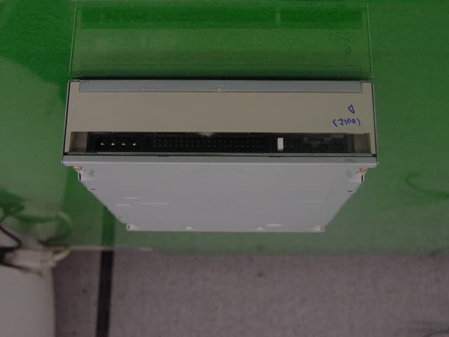
Click to zoom
Application Details
- Equipment Class
- JBP - Part 15 Class B Computing Device Peripheral
- Date of Grant
- Jul 29, 2002
- Application Purpose
- Original Equipment
- Date of Application
- Jul 29, 2002
- Equipment Note
- Internal CD-R/RW Drive
- Company
- Samsung Electronics Co Ltd
- Country
- United States
Documents & Files
Document Text
Text extracted from the exhibit documents filed with the FCC. Open a document above to read the original.
Users Manual
• Specifications • Cautions at Service • External Part Name • Necessary equipments and Specifications in needing Service(P/U replacement) • Exploded Views & Part List • Packing Options • Block Diagram • Troubleshooting • Circuit Diagram • Main Components Block Diagram & Pin Descriptions • Electrical Parts List The design and part of this product is subject to change without prior notice for performance improvement. CONTENTS SERVICE Manual SW-248B CD-R/RW DRIVE 1 1. General Specifications - Drive type : Computer built-in - Power consumption : DC +5V, 1.5A DC +12V, 1.5A - Dimensions : 146mm (W)X42mm (H)X184mm (L) - Net Weight : 750g 2. Electrical Features - Interface : ATAPI BUS(IDE) - Data transfer rate : Write(CD-R) : 600KBytes/Sec(4X) 1,200KBytes/Sec(8X) 1,800KBytes/Sec(12X) 2,400KBytes/Sec(16X) 3,000KBytes/Sec(20X) 3,600KBytes/Sec(24X) 4,200KBytes/Sec(28X) 4,800KBytes/Sec(32X) Write(CD-RW) : 600KBytes/Sec(4X) Write(High Speed CD-RW) : 600KBytes/Sec(4X) 1,500KBytes/Sec(10X) Resd(MAX) : 2,000~6,000KBytes/Sec(CAV 40X) - Access time : 110ms (Random. TYPICAL) - Buffer Capacity : 8Mbyte - Error ratio : Mode 1: Below 10 -12 Mode 2: Below 10 -9 - Frequency response : 20Hz~20kHz (Lineout) 100Hz~20kHz (H/P out) - Signal to noise ratio : 70dB(1kHz, Lineout) - Distortion factor : 0.15% Less than(1KHz) - Channel separation : 65dB(1kHz, Lineout) 55dB(1kHz, H/P out) - Used laser : Semiconductor laser - Audio Output : Line out 0.75 ±20%(Vrms), 47KΩ H/P out 0.65 ±20%(Vrms), 33Ω 1. General Items 1) Be careful not to have your eyes or a part of body touch with- laser diode at repair because this product uses laser diode. 2) Do not disassemble Pick-up at repair. If the laser diode is bad, replace the entire Pick-up. 3) Keep away from TV or other electrical units at repair to prevent influence from surrounding units. 4) If you replace the parts during repair, be sure to unplug the power cable before replacement. 5) If you insert a disc into the drive, be sure to load it corectly. 6) Because this unit can't be used by itself, surely mount it on PC (586 DMA support) and check the operations in use of private device driver floppy diskette. Refer to Instruction manual. 7) This unit has many parts with features related to safety and especially, for essential parts, the importance is indicated on circuit diagram and part list. Be certain to use the parts with same specifications at replaing these parts. 2. Earthing cautions at handling Pick-up - Because the laser diode in optical Pick-up is subject to get out of order due to the potential difference occurring by electricity load charged in clothes or bodies, observe the following earthing items at handling. 1) Body earthing(hand) : Be sure to wear a wrist strip with one side earthed.(Impedance : Below 104). It removes the electricity formed in body. 2) Work table earthing : Put the earthed conductive plate (Impedance : Below 104) such as copper plate on work table. 3) Cautions for clothes : Do not have any clothes touch with Pick-up because the electricity formed in clothes is destroyed easily. Specifications Cautions at Service 2 Electricity sensing device Safety instructions Some semiconductor units may be damaged easily by electricity. These elements are called as electricity sensing device(ESD) in general. For example, integrated circuit, field effect transister, semiconductor chip. The following methods have to be used to reduce the accident of element damage generated by electricity. 1) Emit all electric charges in your body through contact with earthing materail at once before handling a semiconductor factor or device including it. In other way, make use of commercial wristlet against electricity It shall be detached before power impression to the unit on testing because of shock. 2) After detaching an electrical device including ESD, it shall be placed on conductive surface such as aluminium to prevent the charge acummulation and unit exposure. 3) Utilize only the soldering iron with earthed end for ESD soldering or release 4) Make use of only anti-static soldering release unit. A soldering release unit not to be classified as antistatic may generate the enough charge to damage ESD unit. 5) Never use a Freon-propelling chemical product. It may generate the enough charge to damage ESD. 6) Untill installing ESD unit for replacement, never it from protection package. (Most of ESD unit for replacement have lead composed of package shorted electrically by conductive foam, aluminium or similar conductive material.) 7) Contact with shassis including ESD or protection material in circuit parts just before detaching the protection material from lead of ESD unit for replacement 8) Minimize the body action at handling an unpacked ESD unit for replacement. (Otherwise, an unconscious action, so to speak, friction between clothes or foot lifting from carpet floor may generate the enough charge to damage ESD unit.) Note: Be sure to avoid the power impression to the shassis or circuit and observe the safety instruction. 1) Read all safety and operational manuals before operating this product 2) Keep the safety and operational manuals for future reference. 3) Observe all precations and operational instructions in or on the surface of this product. 4) Follow all operation and maintenance cautions. 5) Be sure to plug off the power cable before cleaning. Use a dry cloth to clean a dusty cover of cabinet instead of liquid or aersol cleaner. 6) Never use a attachment not to be recommended by this company. It may result in danger and damage. 7) Never use this product around water such as bathtub, washbasin, laundry machine, swimming pool or lakeside. 8) Never place this product on bed, sofa or around radiator and heater. 9) Power : Utilize the only power displayed on lebel If the power type can't be checked, call to dealer or Korea Electricity, Co, Ltd. Refer tooperate this product by battery or other power. 10) Lightning : Plug off the power cable for product protection durin…
Text truncated - open the document above for the full version.
Users Manual
26 Main Components Block Diagram and Pin Descrition RL3E804 27 RL3E804 28 RL3E804 29 RL3E804 30 RL3E804 31 RL3E804 32 RL3E804 33 RL3E804 34 RL3E804 35 RL3E804 36 RL3E804 37 RL3E804 38 RL3E804 39 RL3E804 40 RL3E804 41 Pin Functions in Each Operating Mode Pin No.Pin Name TFP-100B 1 2 3 4 5 6 7 8 9 10 11 12 13 14 15 16 17 18 19 20 21 22 23 24 25 26 27 28 29 30 31 32 33 34 35 36 37 38 39 40 41 42 43 44 45 46 47 48 3 4 5 6 7 8 9 10 11 12 13 14 15 16 17 18 19 20 21 22 23 24 25 26 27 28 29 30 31 32 33 34 35 36 37 38 39 40 41 42 43 44 45 46 47 48 49 50 P12/TIOCC0/ TCLKA/A22 P13/TIOCD0/ TCLKB/A23 P14/TIOCA1 P15/TIOCB1/ TCLKC P16/TIOCA2 P17/TIOCB2/ TCLKD V SS P30/TxD0 P31/TxD1 P32/RxD0 P33/RxD1 P34/SCK0/IRQ4 P35/SCK1/IRQ5 PE0/D0 PE1/D1 PE2/D2 PE3/D3 V SS PE4/D4 PE5/D5 PE6/D6 PE7/D7 D8 D9 D10 D11 D12 D13 D14 D15 V SS A0 A1 A2 A3 A4 A5 A6 A7 V CC A8 A9 A10 A11 A12 A13 A14 A15 P12/TIOCC0/ TCLKA/A22 P13/TIOCD0/ TCLKB/A23 P14/TIOCA1 P15/TIOCB1/ TCLKC P16/TIOCA2 P17/TIOCB2/ TCLKD V SS P30/TxD0 P31/TxD1 P32/RxD0 P33/RxD1 P34/SCK0/IRQ4 P35/SCK1/IRQ5 PE0/D0 PE1/D1 PE2/D2 PE3/D3 V SS PE4/D4 PE5/D5 PE6/D6 PE7/D7 D8 D9 D10 D11 D12 D13 D14 D15 V SS A0 A1 A2 A3 A4 A5 A6 A7 V CC A8 A9 A10 A11 A12 A13 A14 A15 P12/TIOCC0/ TCLKA/A22 P13/TIOCD0/ TCLKB/A23 P14/TIOCA1 P15/TIOCB1/ TCLKC P16/TIOCA2 P17/TIOCB2/ TCLKD V SS P30/TxD0 P31/TxD1 P32/RxD0 P33/RxD1 P34/SCK0/IRQ4 P35/SCK1/IRQ5 PE0/D0 PE1/D1 PE2/D2 PE3/D3 V SS PE4/D4 PE5/D5 PE6/D6 PE7/D7 D8 D9 D10 D11 D12 D13 D14 D15 V SS PC0/A0 PC1/A1 PC2/A2 PC3/A3 PC4/A4 PC5/A5 PC6/A6 PC7/A7 V CC PB0/A8 PB1/A9 PB2/A10 PB3/A11 PB4/A12 PB5/A13 PB6/A14 PB7/A15 FP-100A4 Mode 5 Mode 6 *1 Mode P12/TIOCC0/ TCLKA P13/TIOCD0/ TCLKB P14/TIOCA1 P15/TIOCB1/ TCLKC P16/TIOCA2 P17/TIOCB2/ TCLKD V SS P30/TxD0 P31/TxD1 P32/RxD0 P33/RxD1 P34/SCK0/IRQ4 P35/SCK1/IRQ5 PE0 PE1 PE2 PE3 V SS PE4 PE5 PE6 PE7 PD0 PD1 PD2 PD3 PD4 PD5 PD6 PD7 V SS PC0 PC1 PC2 PC3 PC4 PC5 PC6 PC7 V CC PB0 PB1 PB2 PB3 PB4 PB5 PB6 PB7 7 *1 Mode NC NC NC NC NC NC V SS NC NC NC NC NC NC NC NC NC NC V SS NC NC NC NC FO0 FO1 FO2 FO3 FO4 FO5 FO6 FO7 V SS A0 A1 A2 A3 A4 A5 A6 A7 V CC A8 A9 A10 A11 A12 A13 A14 A15 Flash Memory Programmer Mode *2 42 Pin Functions in Each Operating Mode Pin No.Pin Name TFP-100B 49 50 51 52 53 54 55 56 57 58 59 60 61 62 63 64 65 66 67 68 69 70 71 72 73 74 75 76 77 78 79 80 81 82 83 84 85 86 87 88 89 90 91 51 52 53 54 55 56 57 58 59 60 61 62 63 64 65 66 67 68 69 70 71 72 73 74 75 76 77 78 79 80 81 82 83 84 85 86 87 88 89 90 91 92 93 V SS A16 A17 A18 A19 P20/TIOCA3 P21/TIOCB3 P22/TIOCC3/ TMRI0 MD0 MD1 P23/TIOCD3/ TMCI0 WDTOVF (FWE, EMLE) *3 MD2 RES NMI STBY V CC XTAL EXTAL V SS PF7/ø PF6/AS RD HWR PF3/LWR/IRQ3 PF2/WAIT/ IRQ2/DREQO PF1/BACK/ IRQ1/CS5 PF0/BREQ/ IRQ0/CS4 AV CC Vref P40/AN0 P41/AN1 P42/AN2 P43/AN3 P44/AN4 P45/AN5 P46/AN6/DA0 P47/AN7/DA1 AV SS VSS P24/TIOCA4/ TMRI1 P25/TIOCB4/ TMCI1 P26/TIOCA5/ TMO0 V SS A16 A17 A18 A19 P20/TIOCA3 P21/TIOCB3 P22/TIOCC3/ TMRI0 MD0 MD1 P23/TIOCD3/ TMCI0 WDTOVF (FWE, EMLE) *3 MD2 RES NMI STBY V CC XTAL EXTAL V SS PF7/ø PF6/AS RD HWR PF3/LWR/IRQ3 PF2/WAIT/ IRQ2/DREQO PF1/BACK/ IRQ1/CS5 PF0/BREQ/ IRQ0/CS4 AV CC Vref P40/AN0 P41/AN1 P42/AN2 P43/AN3 P44/AN4 P45/AN5 P46/AN6/DA0 P47/AN7/DA1 AV SS VSS P24/TIOCA4/ TMRI1 P25/TIOCB4/ TMCI1 P26/TIOCA5/ TMO0 VSS PA0/A16 PA1/A17 PA2/A18 PA3/A19 P20/TIOCA3 P21/TIOCB3 P22/TIOCC3/ TMRI0 MD0 MD1 P23/TIOCD3/ TMCI0 WDTOVF (FWE, EMLE) *3 MD2 RES NMI STBY V CC XTAL EXTAL V SS PF7/ø PF6/AS RD HWR PF3/LWR/IRQ3 PF2/WAIT/ IRQ2/DREQO PF1/BACK/ IRQ1/CS5 PF0/BREQ/ IRQ0/CS4 AV CC Vref P40/AN0 P41/AN1 P42/AN2 P43/AN3 P44/AN4 P45/AN5 P46/AN6/DA0 P47/AN7/DA1 AV SS VSS P24/TIOCA4/ TMRI1 P25/TIOCB4/ TMCI1 P26/TIOCA5/ TMO0 FP-100A4 Mode 5 Mode 6 * 1 Mode VSS PA0 PA1 PA2 PA3 P20/TIOCA3 P21/TIOCB3 P22/TIOCC3/ TMRI0 MD0 MD1 P23/TIOCD3/ TMCI0 WDTOVF (FWE, EMLE) *3 MD2 RES NMI STBY V CC XTAL EXTAL V SS PF7/ø PF6 PF5 PF4 PF3/IRQ3 PF2/IRQ2 PF1/IRQ1 PF0/IRQ0 AVCC Vref P40/AN0 P41/AN1 P42/AN2 P43/AN3 P44/AN4 P45/AN5 P46/AN6/DA0 P47/AN7/DA1 AV SS VSS P24/TIOCA4/ TMRI1 P25/TIOCB4/ TMCI1 P26/TIOCA5/ TMO0 7 * 1 Mode V SS A16 A17 A18 NC OE CE WE V SS VSS VCC FWE V SS RES V CC VCC V CC XTAL EXTAL V SS NC NC NC NC NC V CC VSS VSS VCC VCC NC NC NC NC NC NC NC NC V SS VSS NC VSS NC Flash Memory Programmer Mode * 2 43 Pin Functions in Each Operating Mode Notes : 1. Only modes 4 and 5 are available on the ROMless version. 2. Flash memory programmer mode information is preliminary. 3. The FWE pin function is only available on the H8S/2318 F-ZTAT and H8S/2315 F-ZTAT versions. The EMLE pin function is only available on the H8S/2319 F-ZTAT version. It cannot be used as a WDTOVF pin on the F-ZTAT version. Pin No.Pin Name TFP-100B 92 93 94 95 96 97 98 99 100 94 95 96 97 98 99 100 1 2 P27/TIOCB5/ TMO1 PG0/IRQ6/ ADTRG PG1/CS3/ IRQ7/CS6 PG2/CS2 PG3/CS1/CS7 PG4/CS0 V CC P10/TIOCA0/A20 P11/TIOCB0/A21 P27/TIOCB5/ TMO1 PG0/IRQ6/ ADTRG PG1/CS3/ IRQ7/CS6 PG2/CS2 PG3/CS1/CS7 PG4/CS0 V CC P10/TIOCA0/A20 P11/TIOCB0/A21 P27/TIOCB5/ TMO1 PG0/IRQ6/ ADTRG PG1/CS3/ IRQ7/CS6 PG2/CS2 PG3/CS1/CS7 PG4/CS0 V CC P10/TIOCA0/A20 P11/TIOCB0/A21 FP-100A4 Mode 5 Mode 6 * 1 Mode P27/TIOCB5/ TMO1 PG0/IRQ6/ ADTRG PG1/IRQ7 PG2 PG3 PG4 V CC P10/TIOCA0 P11/TIOCB0 7 * 1 Mode NC NC NC NC NC NC V CC NC NC Flash Memory Programmer Mode * 2 44 BD7902CFS 45 BD7902CFS Pin Descriptions 1HU+Hall amp.U positive input54DVCCPWM block control power supply 2HU-Hall amp.U negative input53FCINFocus driver input 3HV+Hall amp.U positive input52TKINTracking driver input 4HV-Hall amp.U negative input51VCCBTL pre and Loading power supply 5HW+Hall amp.U positive input50LDO+Loading driver positive output 6HW-Hall amp.U negative input49LDO-Loading driver negative output 7HBHall bias48TKO+Tracking driver positive output 8PGND1Spindle driver power ground147TKO-Tracking driver negative output 9USpindle driver output U46FCO+Focus driver positive output 10SPVM1Spindle driver power supply145FCO-Focus driver negative output 11VSpindle driver output V44AVMActuator driver block power supply 12GNDGND43GNDGND 13GNDGND42GNDGND 14GNDGND41GNDG…
Text truncated - open the document above for the full version.
Block Diagram
Deck Mechanism Pick-up LD&MDPD&RFActuator Spindle MOTOR Step MOTOR Solenoide CXA2649R Analog Signal processor - AGC & RFEqualizer- Servo Signal Generator-ATI PPROCESS-RFE QUALIZER-FOCUS & TRACKING ERROR GENERATE - APC 5V GND 5V E - IDEBUS LINEOUT POWER HOST I/F -ATAPIHOSTI/F-ATIPI/F - SUBCODE PROCESS-BUFFER(DRAM)CONTROL- SYSTEM CONTROL BD7907FS -ActuatorDrive-SpindleDrive-SLEDmotorDrive Loading MOTORDrive STAND-BY ) MECHA part STAND-BY Block Diagram RF Signal processor CD-R/RWENDEC OTI9797 H8S/2392 SLEEP I/F, CPU Part SLEEP MODE - PLL- EFM DEMODULATION-EFM+DEMODULATION-BCAREADSUPPORT-CLV/CAVCONTROL-SERVOCONTROL U-COM DRAM(8M) M12L64164A - ESMT K4S641632F - SEC HY29F400ABT - Hynix M29F400BB - ST FLSH (4 M ) DATA BUS
Internal Photos
SET PCB PCB
Test Report
Page 1 of 12 Project NO. : LBE020379 Project NO. : LBE020379 Product :CD-R/RW Drive Model No. :SW-248(VER:B) Date of test :June 29, 2002 - July 03, 2002 Issued Date :July 04, 2002 Tested by: Choon Kil, Kim / Test Engineer Reviewed by: Yang Soo, KIM / Technical Manager Authorized by: Kyu Baek, CHUNG / Chief of EMC Lab. SAMSUNG ELECTRONICS Co., Ltd. Suwon EMC Test Laboratory 416 Maetan-3 Dong, Paldal-Ku, Suwon City, Kyungki-Do, Korea,442-742 Tel. : 81-31-200-2185 Fax. : 81-31-200-2189 This report shall not be reproduced except in full, without the written approval of SEC EMC Testing laboratory. EMC TEST REPORT According to FCC Part 15B Class B Page 2 of 12 Project NO. : LBE020379 Table of Contents 1. General Information 1.1 Product Description 1.2 System Block Diagram of Test Configuration 2. System Test Configuration 2.1 Configuration of Radiated and Conducted Interference Measurement 2.2 Operation Enviroment 2.3 Justification 2.4 EUT Exercise Soft ware 2.5 Test Procedure 3. Conducted Emission Test Data 4. Radiated Emission Test Data 5. Test Equipment Used This report shall not be reproduced except in full, without the written approval of SEC EMC Testing laboratory. Page 3 of 12 Project NO. : LBE020379 1. General Information APPLICANT :SAMSUNG ELECTRONICS CO., LTD. ADDRESS :416 Maetan 3 Dong, Paldal-Ku, Suwon City, Kyungki Do, Korea, 442-742 CONTACT ADDRESS :416 Maetan 3 Dong, Paldal-Ku, Suwon City, Kyungki Do, Korea, 442-742 CONTACT PERSON :Ki Ho,Kim REGULATION(S) :FCC Part 15B Class B MODEL NUMBER:SW-248(VER:B) SERIAL NUMBER :- KIND OF PRODUCT :CD-R/RW Drive TESTED DATE :June 29, 2002 - July 03, 2002 TEST SITE :SAMSUNG EMC TEST LAB. FCC Registration Number : 98856 Anechoic Chamber #1 This report shall not be reproduced except in full, without the written approval of SEC EMC Testing laboratory. Page 4 of 12 Project NO. : LBE020379 1.1 Product Description SpeedCD-R : 48X, CD-RW : 16X, CD-ROM:48X Access Time CD-ROM(110ms) , CD-RW(110ms) Buffer8MB Interface ATAPI (E-IDE) Size 1.2 System Block Diagram of Test Configuration This report shall not be reproduced except in full, without the written approval of SEC EMC Testing laboratory. 148.2(W) * 42(H) * 184(D) mm E B C D A AC POWER AC POWER 1 2 3 4 5 F 6 Page 5 of 12 Project NO. : LBE020379 2.5.2 Configuration of EUT and peripherals MarkItemModel No.Serial No.ManufacturerRemark ACD-R/RW DriveSW-248(VER:B)-SamsungEUT BComputerVectva XE310 FR12634657 HP CLCD MonitorCX-151S N192H4NT319256 Samsung DKeyBoardKB-9963 3892A569 Compaq EMouseM-S09 3892D101 Compaq FEar Phone- -- 2.5.3 Used Cable Description No.ItemLength[m]Shielded(Y/N) 1AC Power Cable1.7N 2Video Cable1.8Y 3Mouse Cable2.0N 4Keyboard Cable1.8N 5AC Power Cable1.7N 6Ear Phone Cable2.0N This report shall not be reproduced except in full, without the written approval of SEC EMC Testing laboratory. Remark Page 6 of 12 Project NO. : LBE020379 2. System Test Configuration 2.1 Configuration of Radiated and Conducted Interference Measurement * Cabling was taken into consideration and test data was taken under worse case conditions. 1)Conduction(Front View) 2)Conduction(Rear View) This report shall not be reproduced except in full, without the written approval of SEC EMC Testing laboratory. Page 7 of 12 Project NO. : LBE020379 3) Radiation(Front View) 4) Radiation(Rear View) This report shall not be reproduced except in full, without the written approval of SEC EMC Testing laboratory. Page 8 of 12 Project NO. : LBE020379 2.2 Operation Enviroment ConductionRadiation Temperature [centigrade] :2323 Humidity [%] :5243 Power supply :AC120V/60HzAC120V/60Hz 2.3 Justification The system was configured in typical fashion(as a customer would normally use it) for testing. 2.4 EUT Exercise Soft ware The EUT exercise program used during radiated and conducted testing was designed to exercise the various system components in a manner similar to typical use. 2.5 Test Procedure 2.5.1 Conducted Emissions Eut was placed on a platform of nominal size, 1m by 1.5m, raised 80cm above the conducting ground plane. The rear of tabletop was located 40cm to the vertical conducting ground plane. The rear of EUT,including peripherals was aligned and flush with rear of tabletop. All other surfaces of tabletop was at least 80cm from any other grounded conducting surface. I/O cables and AC cables that were connected to the peripherals were bundled in center. They were folded back and forth forming a bundle 30cm to 40cm long and were hanged at a 40cm height to the ground plane. Each EUT current-carrying power lead,except the ground(safety) lead, were individually connected through a LISN to the input power source. This report shall not be reproduced except in full, without the written approval of SEC EMC Testing laboratory. Page 9 of 12 Project NO. : LBE020379 All unused 50 ohm connectors of the LISN were resistively terminated in 50 ohm when not connected to the measuring equipment. 2.5.2 Radiated Emissions Eut was placed on a platform of nominal size, 1m by 1.5m, raised 80cm above the conducting ground plane. The rear of EUT,including peripherals was aligned and flush with rear of tabletop. I/O cables that were connected to the peripherals were bundle in center. They were folded back and forth forming a bundle 30cm to 40cm long and were hanged 40cm height to the ground plane. Test was made with the antenna positioned in both the horizontal and vertical planes of polarization. The measurement antenna was varied in height above the conducting ground plane to obtain the maximum signal strength. This report shall not be reproduced except in full, without the written approval of SEC EMC Testing laboratory. Page 10 of 12 Project NO. : LBE020379 3. Conducted Emission Test Data The initial step in collecting conducted data was to perform a quasi-peak scan over the measurement range using a receiver. The final data represents worst-case emissions. O Test Mode : FrequencyMeter reading(a)TotalResultsLimitsMargin Loss(b)(a) + (b) [MHz]Line(…
Text truncated - open the document above for the full version.
Test Setup Photos
Page 6 of 12 Project NO. : LBE020379 2. System Test Configuration 2.1 Configuration of Radiated and Conducted Interference Measurement * Cabling was taken into consideration and test data was taken under worse case conditions. 1)Conduction(Front View) 2)Conduction(Rear View) This report shall not be reproduced except in full, without the written approval of SEC EMC Testing laboratory. Page 7 of 12 Project NO. : LBE020379 3) Radiation(Front View) 4) Radiation(Rear View) This report shall not be reproduced except in full, without the written approval of SEC EMC Testing laboratory.
Contact Information
Applicant
Jenni Chun(General Manager)
Technical Contact
PCTEST Engineering Lab., Inc.Randy Ortanez
[email protected]410-290-6652
6660-B Dobbin Road · Columbia, Maryland · United States
Test Firm
SAMSUNG ELECTRONICS CO., LTD.No Cheon Park
Technical Specifications
| # | Rule Parts | Frequency Range | Power Output |
|---|---|---|---|
| 1 | 15B | - | - |
Other Applications from Samsung Electronics Co Ltd
A3LSMS741B
Aug 05, 2026Portable Handset
Equipment Class
6VL - 15E 6 GHZ Very Low Power DeviceA3LSMX940
Jul 31, 2026BT,BLE Tablet DTS,UNII a,b,g,n,ac,ax,be and digitizer
Equipment Class
DTS - Digital Transmission SystemA3LSMS741U
Jul 30, 2026Portable Handset
Equipment Class
6CD - 15E 6 GHz Low Power Dual ClientA3LSMX840
Jul 27, 2026BT,BLE Tablet DTS,UNII a,b,g,n,ac,ax and Digitizer
Equipment Class
DSS - Part 15 Spread Spectrum TransmitterA3LSMX848U
Jul 27, 2026WCDMA, LTE, 5G NR Tablet BT,BLE, DTS,UNII a b g n ac ax and Digitizer
Equipment Class
JBP - Part 15 Class B Computing Device Peripheral