A3LUM100Wireless USB Mini-Card UWB Transmitter Module
Samsung Electronics Co Ltd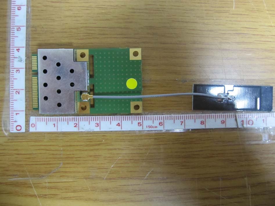
Click to zoom
Application Details
- Equipment Class
- UWB - Ultra Wideband Transmitter
- Date of Grant
- Feb 07, 2011
- Application Purpose
- Original Equipment
- Date of Application
- Jan 02, 2011
- Equipment Note
- Wireless USB Mini-Card UWB Transmitter Module
- Frequency Range
- 7392.00000000 - 8976.00000000
- Company
- Samsung Electronics Co Ltd
- Country
- United States
Documents & Files
Document Text
Text extracted from the exhibit documents filed with the FCC. Open a document above to read the original.
Users Manual
UM100 Wireless USB Radio Card Revision 1.00 Dec. 2010 U U s s e e r r s s G G u u i i d d e e 2010 Samsung Electronics Co., Ltd. All rights reserved. USERS GUIDE_REV1.00 2 1 INTRODUCTION The UM100 PCB Radio module is a complete compact device radio reference design that enables quick design of UWB enabled products. The UM100 combines the Samsung UWB chipset (S3C2680A, S5M8311X) along with on board power supplies, an antenna output and a USB 2.0 system interface. USERS GUIDE_REV1.00 3 2 REFERENCE DESIGN FEATURES • Optimized Performance with S5M8311X (3.1GHz to 8.976GHz) WiMedia BG#1, 3, 6 • Complete Baseband Processor (BBP) and Media Access Controller (MAC) • High Precision Data Path and Data Converters allowing reliable link at extended ranges • Fully Integrated MAC Protocol Engine Supports All Industry Standards WiMedia protocols - Certified Wireless USB - WiMedia Link Layer Protocol • Industry Standard Interfaces - USB 2.0 – Data • Operates from a single (+3.3 V) supply • Small Form Factor (Mini-card form factor) • 5 GPIO lines for additional system control signals USERS GUIDE_REV1.00 4 3 USAGE AND DOCUMENTATION The UM100 is a complete, self-contained UWB radio module requiring only +3.3V regulated power from the host system and providing USB 2.0 interface to the host system for data and the WUSB association function. The UM100 is intended to provide a simple path for a wired USB product design to migrate to a UWB enabled wireless USB product design. The UM100 is a wireless USB certified platform and will have received FCC approval as a Modular UWB transmitter under subpart F of the FCC rules. The product implementation will be able to apply these approvals to the product which incorporates the UM100. This document provides an outline of the purpose and functionality provided by the UM100, complete information for the product system designer is contained in the Samsung UWB Chipset H/W Design Guide. USERS GUIDE_REV1.00 5 4 USER I/O INTERFACE 4.1 DESIGN RECOMMENDATION AND GUIDE USERS GUIDE_REV1.00 6 5 DESIGN CONSIDERATIONS 5.1 POWER One +3.3 V power supply at max data rate average current of 120mA with peak at 180mA. Connector pins #2, 24 and 52 (+3.3V) are connected in common, all these should connect to the host system power rail. Connector pins #4, 9, 15, 18, 21, 26, 27, 29, 34, 35, 40, and 50 are connected in common, all should connect to the host system ground. 5.2 UWB ANTENNA The UM100 will have received FCC approval when employed one antenna below. • INPAQ (Taiwan) model number WA-P-UWB This is the only antenna to be approved by the FCC for use with the Samsung UM100, any substitution of any other antenna automatically invalidates the FCC approval. USERS GUIDE_REV1.00 7 6 MECHANICAL Recommended connector: Molex 67910-0002 PCI Express Mini Card Connector with Molex 48099-4000 PCI Express Mini Card Latch. USERS GUIDE_REV1.00 8 7 FCC STATEMENT This equipment has been tested and found to comply with the limits for a Class B digital device, pursuant to Part 15 of the FCC Rules. These limits are designed to provide reasonable protection against harmful interference in a residential installation. This equipment generates, uses and can radiate radio frequency energy and, if not installed and used in accordance with the instructions, may cause harmful interference to radio communications. However, there is no guarantee that interference will not occur in a particular installation. If this equipment does cause harmful interference to radio or television reception, which can be determined by turning the equipment off and on, the user is encouraged to try to correct the interference by one of the following measures: ● Reorient or relocate the receiving antenna. ● Increase the separation between the equipment and receiver. ● Connect the equipment into an outlet on a circuit different from that to which the receiver is connected. ● Consult the dealer or an experienced radio/TV technician for help. FCC Caution: Any changes or modifications not expressly approved by the party responsible for compliance could void the user's authority to operate this equipment. This device complies with Part 15 of the FCC Rules. Operation is subject to the following two conditions: (1) This device may not cause harmful interference, and (2) this device must accept any interference received, including interference that may cause undesired operation. USERS GUIDE_REV1.00 9 This device and its antenna(s) must not be co-located or operation in conjunction with any other antenna or transmitter. A UWB device operating under the provisions of this section shall transmit only when it is sending information to an associated receiver. The UWB intentional radiator shall cease transmission within 10 seconds unless it receives an acknowledgement from the associated receiver that its transmission is being received. An acknowledgement of reception must continue to be received by the UWB intentional radiator at least every 10 seconds or the UWB device must cease transmitting.
Attestation Statements
Samsung Electronics Co., Ltd. San #24 Nongseo-Dong, Giheung-Gu Yongin-City, Gyeonggi-Do, Korea 446-711 TEL : (82)-(31)-209-6546 FAX : (82)-(31)-209-3131 December 10, 2010 Federal Communications Commission Equipment Authorization Branch 7435 Oakland Mills Road Columbia, MD 21046 LETTER OF AUTHORIZATION To whom it may concern: We, the undersigned, hereby authorize LTA Co., Ltd., to act on our behalf in all manners relating to application for equipment authorization for FCC ID: A3LUM100 . including signing of all documents relating to these matters. Any and all acts carried out by LTA Co., Ltd., on our behalf shall have the same affect as acts of our own. This authorization is valid until further written notice from Samsung Electronics Co., Ltd. LTA Co.,LTD. (Contact Person) Contact name: LEE, Kyung-Taek Position: Manager Phone:(82)31-323-6008 E-mail: [email protected] Regards, Peter Ra General Manager Samsung Electronics America INC.
Cover Letter(s)
Samsung Electronics Co., Ltd. San #24 Nongseo-Dong, Giheung-Gu Yongin-City, Gyeonggi-Do, Korea 446-711 TEL : (82)-(31)-209-6546 FAX : (82)-(31)-209-3131 December 10, 2010 Federal Communications Commission Equipment Authorization Branch 7435 Oakland Mills Road Columbia, MD 21046 In re : Samsung Electonics Co., Ltd. FCC ID: A3LUM100 Request for Confidentiality Pursuant to Sections 0.457 and 0.459 of the Commission’s Rules (CFR 47), and Section 552 (b) (4) of the Freedom of Information Act, Samsung Electronics Co., Ltd. hereby requests confidentiality and treatment of certain information accompanying this application. The materials contain trade secrets and proprietary information not customarily released to the public. The public disclosure of these matters might be harmful to the Applicant and provide unjustified benefits to its competitors. We are also hereby request Short-Term Confidentiality for 180 days after the grant as outlined in Public Notice DA 04-1705. This provision will give Samsung Electronics Co., Ltd. temporary confidentiality of commercially sensitive information prior to product release. The requested Confidential and Temporary Confidential exhibits are listed as follows: Exhibit Type File Name CONFIDENTIAL Schematics CONF APPENDIX A3LUM100 SCH DIA.pdf Parts list CONF APPENDIX A3LUM100 PL.pdf Block diagram CONF APPENDIX A3LUM100 BLK DIA.pdf Operational description CONF APPENDIX A3LUM100 OpDes.pdf SHORT-TERM CONFIDENTIAL External Photos SHORT-TERM CONF A3LUM100 EXT Photo.pdf Internal Photos SHORT-TERM CONF A3LUM100 INT Photo.pdf Test-Setup Photos SHORT-TERM CONF A3LUM100 Test Photo.pdf User’s Manual SHORT-TERM CONF A3LUM100 Manual.pdf The Applicant understands that pursuant to Rule 0.457, disclosure of this application and all accompanying documentations, where applicable, will not be made public before the date of the Grant for this application. Regards, Peter Ra General Manger Samsung Electronics America INC.
Cover Letter(s)
Samsung Electronics Co., Ltd. San #24 Nongseo-Dong, Giheung-Gu Yongin-City, Gyeonggi-Do, Korea 446-711 TEL : (82)-(31)-209-6546 FAX : (82)-(31)-209-3131 FCC ID: A3LUM100 Request for Single Modular Approval Transmitter Module Characteristics The module will be used to the manufac tured product by Samsung Electronics Co., Ltd. No Requirements EUT 1 Have its own RF shielding Device is equipped with metal shielding to cover RF section. Refer to external photos. 2 Have buffered modulation/data inputs (if such inputs are provided) All inputs to the modules are buffered thought logic or microprocessor inputs. 3 Have it own power supply regulation The part number of the power regulator is ( AAT2146 ) 4 Meet the antenna requirements of Section 15.203 The antenna type is PCB antenna. refer to the external photo. 5 Be tested in a stand-alone configuration, i.e., the antenna, AC or DC power and data input/output lines must be connected to the module but, the module must not be inside another case during testing Please reference exhibition Test Conf iguration Photo for the stand-alone test configuration 6 Be labeled with its own FCC ID number, and if the FCC ID is not visible when the module is installed inside another device, then the out side of the device into which the module is installed must also display a label referring to the enclosed module Label is to be placed in front of the EUT(UM 100), and other label is to be placed in the User’s Guide. Refer to FCC ID label format. 7 The modular transmitter is manufactured so t hat the user cannot influence the operation of the transmitter that will operate outsi de of the scope of the regulations. The EUT is compliant whith all applicable FCC rules. Detail instructions for maintaining compliance are given in the Users Manual. 8 Address compliance with the Commission’s RF exposure limits in Sections 1.1310 and 2.1091. In addition, spread spectrum transmitters operating under Section 15.247 are required to address RF exposure compliance in accordance with Section 15.247(b)(4). This device is categorically excluded from routine environmental because it operate at very low power level
External Photos
FCC ID: A3LUM100 Copyright ○ c 2010, LTA Co., Ltd. Page 1 of 2 FCC ID: A3LUM100 Copyright ○ c 2010, LTA Co., Ltd. Page 2 of 2 ANT
ID Label/Location Info
FCC ID: A3LUM100 Copyright Ⓒ 2010, LTA Co., Ltd. SAMPLE LABEL & LOCATION SHIELD CAN FCC ID: A3LUM100 M/N: UM100 Made in Korea
Internal Photos
FCC ID: A3LUM100 Copyright ○ c 2010, LTA Co., Ltd. Page 1 of 2 FCC ID: A3LUM100 Copyright ○ c 2010, LTA Co., Ltd. Page 2 of 2 ANT
Test Report
Ref. No.: LR500111012I Copyright ○ c 2010, LTA Co., Ltd. Page 1 of 36 243 Jubug-Ri,Yangji-Myeon, Yongin-Si, Gyeonggi-Do, Korea 449-822 Tel: +82-31-323-6008 Fax: +82-31-323-6010 http://www.ltalab.com Dates of Tests: December 06~13, 2010 Test Report S/N: LR500111012I Test Site : LTA CO., LTD. CERTIFICATION OF COMPLIANCE FCC ID. APPLICANT Equipment Class : Ultra Wideband Transmitter (UWB) Manufacturing Description : Wireless USB mini-card module Manufacturer : Samsung Electronics Co., Ltd. Model name : UM100 Test Device Serial No.: : Identical prototype Rule Part(s) : FCC Part 15 Subpart F ; ANSI C-63.4-2003 Frequency Range for BG1 : 3168MHz ~ 4752MHz Frequency Range for BG3 : 6336MHz ~ 7920MHz Frequency Range for BG6 : 7392MHz ~ 8976MHz Max. Output Power : Max 86.67dBuV - Radiated Data of issue : December 13, 2010 This test report is issued under the authority of: The test was supervised by: Kyung-Taek LEE, Technical Manager Hyun-Chae You, Test Engineer This test result only responds to the tested sample. It is not allowed to copy this report even partly without the allowance of the test laboratory. This report must not be used by the applicant to claim product endorsement by any agency. NVLAP LAB Code.: 200723-0 A3LUM100 Samsung Electronics Co., Ltd. Ref. No.: LR500111012I Copyright ○ c 2010, LTA Co., Ltd. Page 2 of 36 TABLE OF CONTENTS 1. GENERAL INFORMATION’S -------------------------------------------------------------------------- 2. INFORMATION’S ABOUT TEST ITEM ------------------------------------------------------------- 3. TEST REPORT --------------------------------------------------------------------------------------------- 3.1 SUMMARY OF TESTS ------------------------------------------------------------------------------ 3.2 TECHNICAL CHARACTERISTICS TEST ------------------------------------------------------- 3.2.1 AC CONDUCTED EMISSIONS -------------------------------------------------------------- 3.2.2 Operational limitations ---------------------------------------------------------------------- 3.2.3 UWB Bandwidth Measurement ------------------------------------------------------------ 3.2.4 Radiated Emissions Measurement ----------------------------------------------------------- 3.2.5 Radiated Emissions in GPS Bands Measurement ----------------------------------------- 3.2.6 Peak Emissions within a 10MHz Bandwidth Measurement ------------------------------- APPENDIX APPENDIX TEST EQUIPMENT USED FOR TESTS -------------------------------------------- 3 4 6 6 7 7 8 9 12 26 33 35 Ref. No.: LR500111012I Copyright ○ c 2010, LTA Co., Ltd. Page 3 of 36 1. General information’s 1-1 Test Performed Company name : LTA Co., Ltd. Address : 243, Jubug-ri,Yangji-Myeon,Youngin-Si, Kyunggi-Do, Korea. 449-822 Web site : http://www.ltalab.com E-mail : [email protected] Telephone : +82-31-323-6008 Facsimile +82-31-323-6010 Quality control in the testing laboratory is implemented as per ISO/IEC 17025 which is the “General requirements for the competents of calibration and testing laboratory”. 1-2 Accredited agencies LTA Co., Ltd. is approved to perform EMC testing by the following agencies: Agency Country Accreditation No. Validity Reference NVLAP U.S.A 200723-0 2011-09-30 ECT accredited Lab. RRL KOREA KR0049 2011-06-20 EMC accredited Lab. FCC U.S.A 610755 2011-04-22 FCC filing VCCI JAPAN R2133, C2307 2011-06-21 VCCI registration IC CANADA IC5799 2012-05-14 IC filing Ref. No.: LR500111012I Copyright ○ c 2010, LTA Co., Ltd. Page 4 of 36 2. Information’s about test item 2-1 Client & Manufacturer Company name : Samsung Electronics Co.,Ltd. Address : San #24 Nongseo-Dong, Giheung-Gu, Yongin-City, Gyeonggi-Do 446-711 Korea Tel / Fax : TEL +82-31-209-6546 FAX +82-31-209-3131 2-2 Equipment Under Test (EUT) Trade name : Wireless USB mini-card module FCC ID : A3LUM100 Model name : UM100 Serial number : Identical prototype Date of receipt : December 06, 2010 EUT condition : Pre-production, not damaged Antenna type : PCB Antenna Frequency Range for BG1 : 3168MHz ~ 4752MHz Frequency Range for BG3 : 6336MHz ~ 7920MHz Frequency Range for BG6 : 7392MHz ~ 8976MHz RF output power : Max 86.67dBuV - Radiated Type of Modulation : MB-OFDM Power Source : 3.3Vdc by Main system 2-3 Ancillary Equipment Equipment Model No. Serial No. Manufacturer Notebook PP17L N/A DELL Ref. No.: LR500111012I Copyright ○ c 2010, LTA Co., Ltd. Page 5 of 36 2-4 Description of Test modes Band Group MODE SUB-BAND Frequency (MHZ) 1 1 3432 2 2 3960 3 3 4488 1 4 1,2,3 3432, 3960, 4488 5 1 6600 6 2 7128 7 3 7656 3 8 1,2,3 6600, 7128, 7656 9 1 7656 10 2 8184 11 3 8712 6 12 1,2,3 7656, 8184, 8712 NOTE: After pre-testing each mode, the combination mode (band group 1, 3, 6) was the worst situation and only the data was presented in the following sections <Except for UWB Bandwidth Measurement and Peak Emission Measurement>. Applicable to Description EUT configure mode RE<1G RE≥1G UB PE Frequency (MHZ) 4 √ √ √ √ 3432, 3960, 4488 for BG1 8 √ √ √ √ 6600, 7128, 7656 for BG3 12 √ √ √ √ 7656, 8184, 8712 for BG6 Where RE<1G: Radiated Emission below 1GHz RE≥1G: Radiated Emission above 1GHz UB:UBW Bandwidth PE: Peak Emission Ref. No.: LR500111012I Copyright ○ c 2010, LTA Co., Ltd. Page 6 of 36 3. Test Report 3.1 Summary of tests FCC Part Section(s) Parameter Limit Test Condition Status (note 1) 15.207 AC Conducted Emissions EN 55022 Line Conducted NA note3 15.519(a) Operational Limitations - C 15.519(b) UWB Bandwidth between 3100MHz to 10,600MHz C 15.519(c)/ 15.209 Radiated Emissions Refer to the 3.2.4 C 15.519(d) Radiated Emissions in GPS Bands 19.44dBuV/m at 1M C 15.519(e) Peak Emissions within a 50MHz Bandwidth 90.77dBuV/m at 1M Radiated C 15.203 Antenna requirement - - C Note 1: C=Complies NC=Not Complies NT=Not Tested NA=Not Applicable Note 2: The data in this test report are traceable to the national or international standards. Note 3: This device is only operated by DC Antenna Requirement The Samsung Electronics Co.,Ltd. FCC ID : A3LUM100 unit com…
Text truncated - open the document above for the full version.
Test Setup Photos
FCC ID: A3LUM100 Copyright Ⓒ 2010, LTA Co., Ltd. Radiated Emission (f<1GHz) FCC ID: A3LUM100 Copyright Ⓒ 2010, LTA Co., Ltd. Radiated Emission (f>1GHz)
Contact Information
Applicant
Jenni Chun(General Manager)
Technical Contact
PCTEST Engineering Lab., Inc.Randy Ortanez
[email protected]410-290-6652
6660-B Dobbin Road · Columbia, Maryland · United States
Test Firm
LTA Co.,Ltd.Michael AHN
Technical Specifications
| # | Rule Parts | Frequency Range | Power Output |
|---|---|---|---|
| 3 | 15F | 7.39 GHz - 8.98 GHz | - |
Other Applications from Samsung Electronics Co Ltd
A3LSMS741B
Aug 05, 2026Portable Handset
Equipment Class
6VL - 15E 6 GHZ Very Low Power DeviceA3LSMX940
Jul 31, 2026BT,BLE Tablet DTS,UNII a,b,g,n,ac,ax,be and digitizer
Equipment Class
DTS - Digital Transmission SystemA3LSMS741U
Jul 30, 2026Portable Handset
Equipment Class
6CD - 15E 6 GHz Low Power Dual ClientA3LSMX840
Jul 27, 2026BT,BLE Tablet DTS,UNII a,b,g,n,ac,ax and Digitizer
Equipment Class
DSS - Part 15 Spread Spectrum TransmitterA3LSMX848U
Jul 27, 2026WCDMA, LTE, 5G NR Tablet BT,BLE, DTS,UNII a b g n ac ax and Digitizer
Equipment Class
JBP - Part 15 Class B Computing Device Peripheral