A3LWISP50SAudio Transceiver Module
Samsung Electronics Co Ltd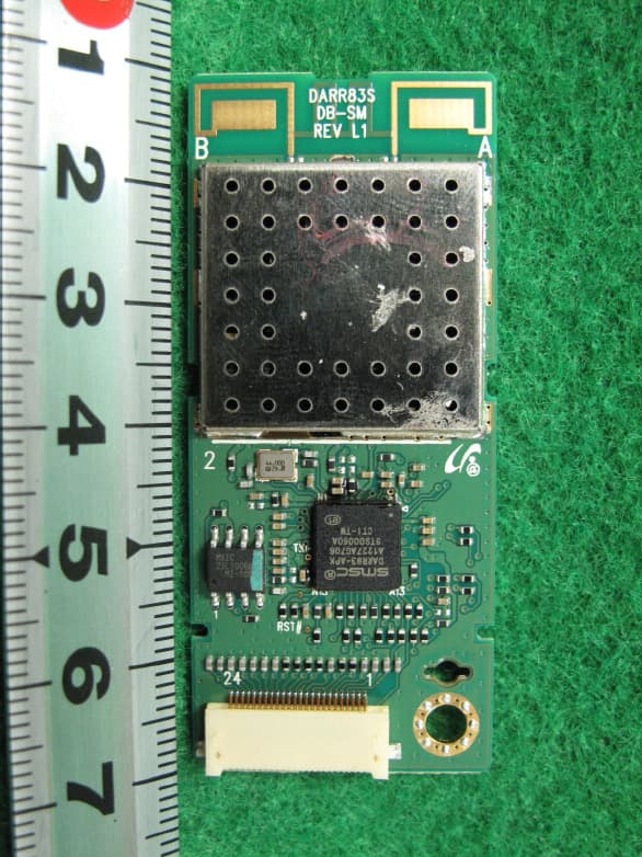
Click to zoom
Application Details
- Equipment Class
- NII - Unlicensed National Information Infrastructure TX
- Date of Grant
- Dec 16, 2012
- Application Purpose
- Original Equipment
- Date of Application
- Dec 16, 2012
- Equipment Note
- Audio Transceiver Module
- Frequency Range
- 5180.00000000 - 5240.00000000
- Company
- Samsung Electronics Co Ltd
- Country
- United States
Documents & Files
Document Text
Text extracted from the exhibit documents filed with the FCC. Open a document above to read the original.
Users Manual
Rev 0.0 Page 1 of 9 WISP50S Module: USER Manual Product Name : Three View Audio Module Model Name : WISP50S Rev 0.0 Page 2 of 9 1. Product Description The WISP50S module is a wireless audio module (60X21mm)) based on the SMSC DARR83. This module can used to build an uncompressed wireless digital audio transceiver operating in the 2.4GHz, 5.2GHz and 5.8GHz bands. The wireless audio link supports up to two stereo audio streams and comes together with additional features such as: data encryption, pairing functionality, bi-directional control data messages, low power audio snooze mode, WLAN detection and Automatic Frequency Allocation. The DARR83 chip itself provides the basic functions of Audio Processing and buffering, Data Link Layer and Physical Layer. The WISP50S module integrates all functionality for a wireless digital and analog audio connection, comprising: 2. Features DARR83 Wireless Audio Processor 2.4GHz/ 5.2GHz/ 5.8 GHz RF Transceiver Embedded Antennas Digital audio interfaces (I 2 S) Integrated 24 bit stereo Audio DAC + Headphone AMP Integrated 16 bit Audio ADC + Microphone AMP Built-in SPI interface Flash 9 pins interface connector for power, audio output, control interface and GPIOs Regulated 5V supply 3. WISP50S Block Diagram Rev 0.0 Page 3 of 9 4. Description of operations 4.1 Operating Conditions ( 5 V 450 mA) Symbol Parameter Min. Typ Max Unit VCC Supply Voltage 4.7 5.0 5.25 V Temp Operating Temperature 0 25 60 °C 4.2 RF Information Parameter Value Unit Modulation QPSK RF Frequency range (band) 2400 – 2483.5 5150 – 5250 5725 – 5875 MHz RF Frequency Ch1 – 2412 Ch2 – 2436 Ch3 – 2464 Ch4 – 5180 Ch5 – 5210 Ch6 – 5240 Ch7 – 5736 Ch8 – 5726 Ch9 – 5814 MHz Audio Latency 20ms Audio Bit Resolution 16bit Audio Sampling Rate 48ksps Note: Country/ Region dependent. 4.3 Receive mode In receive mode, antenna diversity is supported. The single ended output of the TR switch is connected to the RF LNA input through Diplexer and matching networks. Filtering and amplification is all performed by the radio transceiver. The gain setting is controlled by the BB. The analog IQ outputs are sampled by the BB by its integrated 22Msps dual channel 8bit ADC. This received data is demodulated and fed to the audio processing engine controlling the audio function. 4.4 Transmit mode In transmit mode, the audio engine transforms the audio data into packetized digital IQ signals. These are in turn pulse-shaped before conversion by a 10bits 44Msps DAC to match to the analog IQ inputs of the radio IC. The radio IC has programmable baseband filters to lower the RF spectrum side lobes Rev 0.0 Page 4 of 9 and to suppress the DAC image and the DAC spurious. The output power is programmable. A power detector (PD_out) on the radio IC enables close-loop TX power control. The differential RF PA outputs are connected via a baluns and Diplexer to a transmit/receive switch with TX diversity option to the RF connectors. 5. Clock and synthesizer frequencies The main crystal is connected to the Baseband IC crystal oscillator. This in turn buffers this 44MHz and feeds it to the radio IC. In standard configurations, the DARR83 based DWPCIe83 module’s RF section runs at the following frequencies: 2.4GHz Band: The RF oscillator runs at 2 times the programmed RF output frequency. Channel RF frequency (in MHz) VCO frequency (in MHz) 1 2412 4824 2 2438 4876 3 2464 4928 5.2GHz Band: The RF oscillator runs at 2/3 times the programmed RF output frequency. Channel RF frequency (in MHz) VCO frequency (in MHz) 1 5180 3453.33 2 5210 3473.33 3 5240 3493.33 5.8GHz Band: The RF oscillator runs at 2/3 times the programmed RF output frequency. Channel RF frequency (in MHz) VCO frequency (in MHz) 1 5736 3824 2 5762 3841.33 3 5814 3876 6. Modulation Diagram Rev 0.0 Page 5 of 9 7. Pin out interface connector Pin information. Pin Number Pin Name I/ODescription 1 5V PWR Regulated 4.7V to 5.2V input 2 5V PWR Regulated 4.7V to 5.2V input 3 GPIO_2 I/O PWM_RST# 4 GPIO_13 I/O MUTE 5 GPIO_14 I/O POWER_CTL 6 /RESET(DARR_RST) I Reset Darr83 7 I 2 C_SCL_SLV I/O I 2 C serial clock Slave 8 I 2 C_SDA_SLV I/O I 2 C serial data Slave 9 I 2 C_SCL_MST I/O I 2 C serial clock Master 10 I 2 C_SDA_MST I/O I 2 C serial data Master 11 MCLK I/O 12.288MHz audio clock I/O 12 GND GND GND 13 BCK_W I/O I 2 S port W Bit Clock 14 LRCK_W I/O I 2 S port W Left Right Clock 15 GPIO_5 I/O DAT_W 16 GPIO_11 I/O DAT_X 17 MON_TXD I/O Serial sync Data, for test purposes 18 GIPO_6 I/O FW_SEL 19 GPIO_12 I/O IR_RST# 20 GPIO_3 I/O ID_SET# 21 GPIO_15 I/O RED_LED 22 GPIO_4 I/O BLUE_LED (UART_RXD) 23 GPIO_7 I/O IR_SD#(HW_MUTE) 24 GND GND GND Rev 0.0 Page 6 of 9 8. Installation Rev 0.0 Page 7 of 9 9. Notice FCC Statement Federal Communication Commission Interference Statement This equipment has been tested and found to comply with the limits for a Class B digital device, pursuant to Part 15 of the FCC Rules. These limits are designed to provide reasonable protection against harmful interference in a residential installation. This equipment generates, uses and can radiate radio frequency energy and, if not installed and used in accordance with the instructions, may cause harmful interference to radio communications. However, there is no guarantee that interference will not occur in a particular installation. If this equipment does cause harmful interference to radio or television reception, which can be determined by turning the equipment off and on, the user is encouraged to try to correct the interference by one of the following measures: ● Reorient or relocate the receiving antenna. ● Increase the separation between the equipment and receiver. ● Connect the equipment into an outlet on a circuit different from that to which the receiver is connected. ● Consult the dealer or an experienced radio/TV technician for help. FCC Caution: Any changes or modifications not expressly approved by the party responsible for compliance could void the user’s authority to operate this equi…
Text truncated - open the document above for the full version.
Cover Letter(s)
129, Samsung-Ro, Yeongtong-Gu, Suwon-Si, Gyeonggi-Do, KOREA Federal Communications Commission Authorization and Evaluation Division 7435 Oakland Mills Road, Columbia, MD 21046 Date: October 10, 2012 RE: Request of confidentiality for FCC ID: A3LWISP50S To Whom It May Concern: Pursuant to Sections 0.457 and 0.459 of the Commission’s Rules (CFR 47), and Sectio 552 (b) (4) of the Freedom of Information Act, SAMSUNG ELECTRONICS CO.,LTD. Hereby requests confidentiality and treatment of certain information accompanying this application. The materials contain trade secrets and proprietary information not customarily released to the public. The public disclosure of these matters might be harmful to the Applicant and provide unjustified benefits to its competitors. We are also hereby request Short-Term Confidentiality for 180 day after the grant as outlined in Public Notice DA 04-1705. This provision will give SAMSUNG ELECTRONICS CO.,LTD. Temporary confidentiality of commercially sensitive information prior to product release. The requested Permanent and Short-Term Confidential exhibits are listed as follows: PERMANENT AND SHORT-TERM CONFIDENTIAL LIST Exhibit Description PERMANENT 1 Block Diagram 2 Operational Description 3 Schematics SHORT-TERM 4 External Photos 5 Internal Photos 6 Test-Setup Photos 7 Users Manual The Applicant understands that pursuant to Rule 0.457, disclosure of this application and all accompanying documentations, where applicable, will not be made public before the date of the Grant for this application. Sincerely, Name : Sun Kwan Kim Title : S. Manager Company : Samsung Electronics Co., Ltd.
Cover Letter(s)
416, Maethan 3-Dong, Youngtong-Ku, Suwon-City, Kyung-ki-Do, KOREA Attn: Reviewing Engineer Federal communications Commission 7435 Oakland Mills Road Columbia, MD 21046 2011-12-28 RE: PART 15 UNLICENSED MODULAR TRANSMITTER APPROVAL To whom It May Concern: We, Samsung Electronics Co., Ltd., Hereby requests a Modular Approval of our Wireless Audio Transceiver Module, described as follows: Brand name: SAMSUNG Model name: Wireless Audio Transceiver Module FCC ID : A3LWISP50S In FCC Public Notice DA 00-1407 released June 26, 2000 there are eight numbered requirements that our RF Transceiver Module complies with. 1. The modular transmitter must have an own shielding : The radio portion of this module has been shielded, Please see photographs provided with the application. 2. The modular transmitter must have buffered modulation/data inputs. : All inputs to the modules are buffered through logic U1 inputs. Refer to Block Diagram. 3. The modular transmitter must have its own power supply regulation. : The IC Contain an own voltage regulation. In case of changes in the supply voltage VCC (for example caused by temperature changes or other effects), the internal voltage will be stabilized. 4. The modular transmitter must comply with the antenna requirements of Section 15.203 and 15.204c: This module is equipped with an onboard PCB Antenna. For further details please refer to the antenna data sheet included in the filing. 5. The modular transmitter must be tested in a stand-alone configuration: This module was tested in a stand-alone configuration. 6. The modular transmitter must be labeled with its own FCC ID number: This module is labeled with its own FCC ID number, Please see product label design and the external photograph of the device with this label submitted with the application. 7. The modular transmitter must comply with any specific rule of operation requirements applicable to the transmitter and the manufacturer must provide adequate instructions along with the module to explain any such requirements: This module is compliant with all applicable FCC rules. Detail instructions for maintaining compliance are given in the Users Manual. 8. The modular transmitter must comply with any applicable RF exposure requirements: This module is compliant with all applicable RF exposure requirements. RF Exposure is addressed in the test report. Sincerely, Name: Jaywoo Lee Title: Engineer Company: SAMSUNG ELECTRONICS CO., LTD
External Photos
Test Report No.: NK-12-R-170-1 FCC and IC Certification Samsung Electronics Co., Ltd. FCC ID : A3LWISP50S / IC :649E-WISP50S Page 82 of 86 APPENDIX C – EUT PHOTOGRAPHS Front View of EUT Test Report No.: NK-12-R-170-1 FCC and IC Certification Samsung Electronics Co., Ltd. FCC ID : A3LWISP50S / IC :649E-WISP50S Page 83 of 86 Rear View of EUT
ID Label/Location Info
Test Report No.: NK-12-R-170-1 FCC and IC Certification Samsung Electronics Co., Ltd. FCC ID : A3LWISP50S / IC :649E-WISP50S Page 79 of 86 APPENDIX A – LABELLING REQUIREMENTS The sample label shown shall be permanently affixed at a conspicuous location on the device and be readily visible to the user at the time of purchase. ※ See other informations in the manual Labelling Requirements NAMUGA ultimedia Lab A3(420X297) 12 36 WM40 00001 -12 : Year -36: Week -WM40: Model Name -000001: Serial No. -TX F/W edition -L1: PCB edition -V009 : Software edition B: TX L1 V009 PART Art paper 01 A 2:1 NAMUGA PRINT 1:1 VENDER PRINT [X]20mm [X]20mm [X]20mm [X]20mm SAMSUNG Project Shield can white label 9960-WM4001A-0D Seven Seven Jshan Seven Seven Jshan Jshan 2012.09.06 2012.09.06 2012.09.06 JSHan Huang WM40 NOTE: 1. All parts must not contain prohibited substances including ROHS Hazardous substances(Pb, Cd, Hg, Cr++, PBB, PBDE) and for more details refer to NAMUGA’s HSF Requirements Standard) D-QP-QA-015 2. Mark “[x]” dimensions need to be measured. 3. All parts must be halogen free 4. Font type : Arial 5. COLOR - Background : White - Font & Logo : Black Change label information layout Change label size from 18x18mm t0 20x20mm Change label information layout 1236WM4000001 Samsung Electronics Co.Ltd Model : WISP50S TRA FCC ID : A3LWISP50S IC : 649E- WISP50S CMIIT ID: XXXXXXX Part No : AH40-00172A TX L1 V009 NAM-WM40 1 2 3 2012.09.07 2012.10.15 2012.11.08 Registed No. :XXXXXXXX Dealer No. : XXXXXX ICASA : TA-20XX/XXX APPROVED XXXXX/SDPPI/YYYY/NNNN N363 XXXXXXXXXX R Samsung Electronics Co.Ltd Model : WISP50S TRA FCC ID : A3LWISP50S IC : 649E- WISP50S CMIIT ID: XXXXXXX Registed No. :XXXXXXXX Dealer No. : XXXXXX ICASA : TA-20XX/XXX APPROVED XXXXX/SDPPI/YYYY/NNNN N363 XXXXXXXXXX R
Internal Photos
Test Report No.: NK-12-R-170-1 FCC and IC Certification Samsung Electronics Co., Ltd. FCC ID : A3LWISP50S / IC :649E-WISP50S Page 84 of 86 Front View of Mainboard without shielding can
RF Exposure Info
Test Report No.: NK-12-R-170-1 FCC and IC Certification Samsung Electronics Co., Ltd. FCC ID : A3LWISP50S / IC :649E-WISP50S Page 85 of 86 APPENDIX D – Maximum Permissible Exposure RF Exposure Limit According to FCC 1.1310: The criteria listed in the following table shall be used to evaluate the Environmental of human exposure to radio frequency (RF) radiation as specified in 1.1307(b) Limits for Maximum Permissible Exposure (MPE) FrequencyElectric FieldMagnetic Field Power Density Averaging Time Range(MHz)Strength(V/m)Strength(A/m) (mW/cm 2 ) (Minutes) 30 - 30061.40.16316 300 - 1500......F/3006 1500 - 100000......56 30 - 30027.50.0730.230 300 - 1500......F/150030 1500 - 100000......130 (A) Limits for occupational / Contral Exposure (B) Limits for General Population / Uncontrolled Exposure F = Frequency (MHz) Fries formula Fries transmission formula : Pd = (Pout * G) / (4 * π* r²) r = √((Pout * G) / 4 * π* Pd)) Where Pd = Power density in ㎽/㎠ Pout = Output power to antenna in ㎽ G = Gain of antenna in linear scale π= 3.1416 r = Distance between observation point center of the radiator in cm Pd is the limit of MPE, 1 ㎽/㎠. If we know the Maximum Gain of the antenna and the total power input to the antenna, through the calculation, we will know the Maximum distance r where the MPE limit is reached and Power density at prediction frequency. Test Report No.: NK-12-R-170-1 FCC and IC Certification Samsung Electronics Co., Ltd. FCC ID : A3LWISP50S / IC :649E-WISP50S Page 86 of 86 Test Result : 2.4 GHz band The maximum antenna gain is 0.9 dBi. Maximum peak output power at antenna input terminal:16.59 (dBm) Maximum peak output power at antenna input terminal:45.60 (mW) Antenna gain(typical):0.90 (dBi) Maximum antenna gain:1.23 (numeric) Prediction distance:20 (cm) Prediction frequency:2438 (MHz) MPE limit for uncontrolled exposure at prediction frequency:1 (mW/cm^2) Maximum allowable antenna gain:19.41 (dBi) Maximum Distance:2.11 (cm) Power density at prediction frequency : 0.011162(mW/cm^2) Test result: PASS 5.8 GHz band The maximum antenna gain is 6.0 dBi. Maximum peak output power at antenna input terminal:9.11 (dBm) Maximum peak output power at antenna input terminal:8.15 (mW) Antenna gain(typical):6.00 (dBi) Maximum antenna gain:3.98 (numeric) Prediction distance:20 (cm) Prediction frequency:5762 (MHz) MPE limit for uncontrolled exposure at prediction frequency:1 (mW/cm^2) Maximum allowable antenna gain:26.89 (dBi) Maximum Distance:1.61 (cm) Power density at prediction frequency : 0.006453(mW/cm^2) Test result: PASS Test Report No.: NK-12-R-170-2 FCC and IC Certification Samsung Electronics Co., Ltd. FCC ID : A3LWISP50S / IC :649E-WISP50S Page 54 of 54 Test Result : 5.2 GHz band The maximum antenna gain is 2.8 dBi. Maximum peak output power at antenna input terminal:10.20 (dBm) Maximum peak output power at antenna input terminal:10.47 (mW) Antenna gain(typical):2.80 (dBi) Maximum antenna gain:1.91 (numeric) Prediction distance:20 (cm) Prediction frequency:5210 (MHz) MPE limit for uncontrolled exposure at prediction frequency:1 (mW/cm^2) Maximum allowable antenna gain:11.89 (dBi) Maximum Distance:1.26 (cm) Power density at prediction frequency : 0.003969(mW/cm^2) Test result: PASS
Test Report
Test Report No.: NK-12-R-170-2 FCC and IC Certification Samsung Electronics Co., Ltd. FCC ID : A3LWISP50S / IC :649E-WISP50S Page 2 of 54 TABLE OF CONTENTS 1. Scope 4 2. Introduction (Site Description) 5 2.1 Test facility 5 2.2 Accreditation and listing 6 3. Test Conditions & EUT Information 7 3.1 Operation During Test 7 3.2 Support Equipment 7 3.3 Setup Drawing 7 3.4 EUT Information 8 4. Summary of Test Results 9 5. Recommendation / Conclusion 10 6. Antenna Requirements 10 7. Description of Test 11 7.1 Conducted Emissions 11 7.2 Radiated Emissions 12 7.3 26 dB Bandwidth and 99% Occupied Bandwidth 13 7.4 Maximum Peak Output Power 14 7.5 Peak Power Spectral Density 15 7.6 Peak Excursion Measurement 16 7.7 Frequency Stability 17 8. Test Data 18 8.1 Conducted Emissions 18 8.2 Radiated Emissions 21 8.3 26 dB Modulated Bandwidth and 99% Occupied Bandwidth 22 8.4 Peak Power Output 26 8.5 Power Spectral Density 30 Test Report No.: NK-12-R-170-2 FCC and IC Certification Samsung Electronics Co., Ltd. FCC ID : A3LWISP50S / IC :649E-WISP50S Page 3 of 54 8.6 Peak Excursion 34 8.7 Radiated Spurious Emissions 36 8.8 Frequency Stability 43 9 Test Equipment 44 10 Accuracy of Measurement 45 Appendix A: Labelling Requirement 49 Appendix B: Photographs of Test Set-up 50 Appendix C: EUT Photographs 52 Appendix D: Maximum Permissible Exposure 62 Test Report No.: NK-12-R-170-2 FCC and IC Certification Samsung Electronics Co., Ltd. FCC ID : A3LWISP50S / IC :649E-WISP50S Page 4 of 54 1. SCOPE Measurement and determination of electromagnetic emissions (EME) of radio frequency devices including intentional and/or unintentional radiators for compliance with the technical rules and regulations of the Federal Communications Commission under FCC part 15 and IC RSS-210. Responsible Party : Contact Person : Manufacturer : Samsung Electronics Co., Ltd. Mr. Jaywoo. Lee Samsung Electronics Co., Ltd. 129, Samsung-ro, Yeongtong-gu, Suwon-si, Gyeonggi-do, Korea 443-742 FCC ID: A3LWISP50S IC : 649E-WISP50S Model: WISP50S Brand Name: SAMSUNG EUT Type: Audio transceiver module Classification: Unlicensed National Information Infrastructure (UNII) Applied Standard: FCC 47 CFR Part 15 subpart E 15.407 and IC RSS-210 Issue 8 Annex 9 Test Procedure(s): ANSI C63.4-2003, ANSI C63.10 and FCC guidance of 789033 D01 General UNII Test Procedures v01r02 dated September 26, 2012 entitled “Guidelines for Compliance Testing of Unlicensed National Information Infrastructure (U- NII) Devices – Part 15, Subpart E” Dates of Test: October 10, 2012 ~ November 6, 2012 Place of Tests: Nemko Korea Co., Ltd. Test Report No.: NK-12-R-170-2 FCC and IC Certification Samsung Electronics Co., Ltd. FCC ID : A3LWISP50S / IC :649E-WISP50S Page 5 of 54 2. INTRODUCTION 2.1 Test facility The measurement procedure described in American National Standard for Methods of Measurement of Radio-Noise Emissions from Low-Voltage Electrical and Electronic Equipment in the Range of 9 kHz to 40 GHz (ANSI C63.4-2003), the American National Standard for Testing Unlicensed Wireless Devices (ANSI C63.10-2009) was used in determining radiated and conducted emissions emanating from Samsung Electronics Co., Ltd. FCC ID : A3LWISP50S and IC : 649E-WISP50S These measurement tests were conducted at Nemko Korea Co., Ltd. EMC Laboratory . The site address is 155 & 159, Osan-Ro, Mohyeon-Myeon, Cheoin-Gu, Yongin-Si, Gyeonggi-Do 449-852 KOREA, REPULIC OF. The area of Nemko Korea Corporation Ltd. EMC Test Site is located in a mountain area at 80 km (48 miles) southeast and Incheon International Airport (Incheon Airport), 30 km (18miles) south- southeast from central Seoul. It is located in the valley surrounded by mountains in all directions where ambient radio signal conditions are quiet and a favorable area to measure the radio frequency interference on open field test site for the computing and ISM devices manufactures. The detailed description of the measurement facility was found to be in compliance with the requirements of §2.948 according to ANSI C63.4 2003. Fig. 1. The map above shows the Seoul in Korea vicinity area. The map also shows Nemko Korea Corporation Ltd. EMC Lab. and Incheon Airport. Nemko Korea Co., Ltd. EMC Lab. 155 & 159, Osan-Ro, Mohyeon-Myeon, Cheoin-Gu, Yongin-Si, Gyeonggi-Do 449-852 KOREA, REPUBLIC OF Tel)+82-31-330-1700 Fax)+82-31-322-2332 Test Report No.: NK-12-R-170-2 FCC and IC Certification Samsung Electronics Co., Ltd. FCC ID : A3LWISP50S / IC :649E-WISP50S Page 6 of 54 2.2 Accreditation and listing Accreditation type Accreditation number FCC part 15/18 Filing site Registration No. 97992 CAB Accreditation for DOC Designation No. KR0026 KOLAS Accredited Lab. (Korea Laboratory Accreditation Scheme) Registration No. 155 Canada IC Registered site Site No. 2040E VCCI registration site(RE/CE/Telecom CE) Member No. 2118 EMC CBTL - KCC(RRL)Designated Lab. Registration No. KR0026 SASO registered Lab and Certification Body Registration No. 2008-15 Test Report No.: NK-12-R-170-2 FCC and IC Certification Samsung Electronics Co., Ltd. FCC ID : A3LWISP50S / IC :649E-WISP50S Page 7 of 54 3. TEST CONDITIONS & EUT INFORMATION 3.1 Operation During Test The EUT was controlled and monitored by testing Jig which manufacturer supported. The EUT have two antennas which are not working simultaneously. All tests were performed at two antenna paths then the worst case was recorded. The EUT was programmed with the following power setting that used during the testing: Frequency 5180 MHz ~ 5240 MHz Power setting Level 255 3.2 Support Equipment EUT Samsung Electronics Co., Ltd. FCC ID: A3LWISP50S S/N: N/A Laptop Computer HP Model : HSTNN-Q61C 1.2 m shielded USB cable FCC DOC S/N : CNF0489WDT AC/DC Adapter DELTA ELECTRONICS(JIANG SU), LTD Model : PPP009D 1.2 m unshielded power cable FCC DOC S/N :WBGSV0ACXZH162 3.3 Setup Drawing USB EUT AC Adaptor Power Cable I/O Cable Test Jig Laptop Computer Test Report No.: NK-12-R-170-2 FCC and IC Certification Samsung Electronics Co.…
Text truncated - open the document above for the full version.
Test Setup Photos
Test Report No.: NK-12-R-170-1 FCC and IC Certification Samsung Electronics Co., Ltd. FCC ID : A3LWISP50S / IC :649E-WISP50S Page 80 of 86 APPENDIX B – PHOTOGRAPHS OF TEST SET-UP The Conducted Test Picture and Radiated Test Picture and show the worst-case configuration and cable placement. Conducted Test Picture(Front) Conducted Test Picture(Rear) Test Report No.: NK-12-R-170-1 FCC and IC Certification Samsung Electronics Co., Ltd. FCC ID : A3LWISP50S / IC :649E-WISP50S Page 81 of 86 Radiated Test Picture (Front) Radiated Test Picture (Rear)
Contact Information
Applicant
Jenni Chun(General Manager)
Technical Contact
PCTEST Engineering Lab., Inc.Randy Ortanez
[email protected]410-290-6652
6660-B Dobbin Road · Columbia, Maryland · United States
Test Firm
Nemko Korea Co.,Ltd.Hyun-ho Kim
Technical Specifications
| # | Rule Parts | Frequency Range | Power Output |
|---|---|---|---|
| 1 | 15E | 5.18 GHz - 5.24 GHz | 10.00 mW |
Other Applications from Samsung Electronics Co Ltd
A3LSMS741B
Aug 05, 2026Portable Handset
Equipment Class
6VL - 15E 6 GHZ Very Low Power DeviceA3LSMX940
Jul 31, 2026BT,BLE Tablet DTS,UNII a,b,g,n,ac,ax,be and digitizer
Equipment Class
DTS - Digital Transmission SystemA3LSMS741U
Jul 30, 2026Portable Handset
Equipment Class
6CD - 15E 6 GHz Low Power Dual ClientA3LSMX840
Jul 27, 2026BT,BLE Tablet DTS,UNII a,b,g,n,ac,ax and Digitizer
Equipment Class
DSS - Part 15 Spread Spectrum TransmitterA3LSMX848U
Jul 27, 2026WCDMA, LTE, 5G NR Tablet BT,BLE, DTS,UNII a b g n ac ax and Digitizer
Equipment Class
JBP - Part 15 Class B Computing Device Peripheral