AK8-WE8853SBluetooth Module
Sony Group Corporation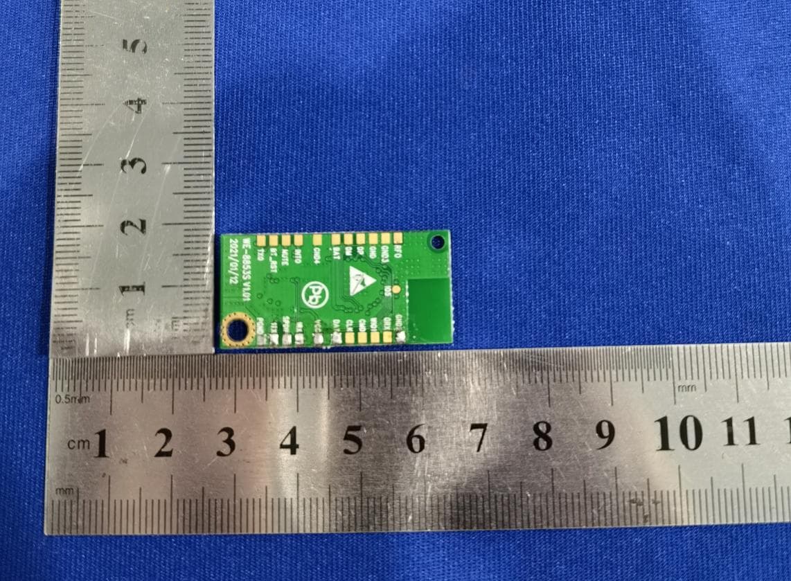
Click to zoom
Application Details
- Equipment Class
- DSS - Part 15 Spread Spectrum Transmitter
- Date of Grant
- Aug 02, 2021
- Application Purpose
- Original Equipment
- Date of Application
- Aug 02, 2021
- Equipment Note
- Bluetooth Module
- Frequency Range
- 2402.00000000 - 2480.00000000
- Company
- Sony Group Corporation
- Country
- Japan
Documents & Files
Document Text
Text extracted from the exhibit documents filed with the FCC. Open a document above to read the original.
Users Manual
This module is compliance with FCC rules part 15 subpart C.
Cover Letter(s)
SONY Sony Group Corporation 1-7-1 Konan Minato-Ku Tokyo, 108-0075 Japan Request form Confidentiality Date: May 13 th , 2021 Federal Communications Commission Authorization and Evaluation Division FCC ID: AK8-WE8853S Applicant: Sony Group Corporation Confidentiality Request Pursuant to Sections 0.457 and 0.459 of the Commission’s Rules, the Applicant hereby requests confidential treatment of information accompanying this application as outlined below: 1. Block diagram 2. Schematics 3. Operation Description The above materials contain trade secrets and proprietary information not customarily released to the public. The public disclosure of these matters might to harmful to the applicant and provide unjustified benefits to its competitors. The applicant understands that pursuant to Rule 0.457, disclosure of this application and all accompanying documentation will not be made before the date of the grant for this application. Sincerely, Takeshi Kobayashi Product Safety Manager Product Compliance Section Quality Assurance Department Sony Corporation. Tel: +81-050-3750-6543 Fax: +81-050-3750-6573 E-mail: [email protected]
Cover Letter(s)
SONY Sony Group Corporation 1-7-1 Konan Minato-Ku Tokyo, 108-0075 Japan Request for Short-Term Confidentiality Date: May 13 th , 2021 Federal Communications Commission Authorization and Evaluation Division FCC ID: AK8-WE8853S. Applicant: Sony Group Corporation To whom it may concern: Please be advised that the following information is to be held in confidence for 180 days from the date of the Grant of Equipment Authorization and behalf of us, referring to the FCC rules 0.457 and 0.459: 1. External Photos 2. Internal Photos 3. Test Setup Photos 4. User manual The application contains technical information, which we deem to be trade secrets and proprietary. If made public, the information might be used to the disadvantage of the applicant in the market place. Thank you for your attention to this matter. Sincerely, Takeshi Kobayashi Product Safety Manager Product Compliance Section Quality Assurance Department Sony Corporation.. Tel: +81-050-3750-6543 Fax: +81-050-3750-6573 E-mail: [email protected]
Cover Letter(s)
Sony Group Corporation Special Power of Attorney I, Kazuyuki Hori of Sony Group Corporation, hereby appoint Takeshi Kobayashi of Sony Corporation to represent me to act on my behalf to do any and all of the following. Sign on my behalf the agency, anti-drug and confidentiality cover letters and apply to FCC for the products. The rights, powers and authority in fact to exercise any and all of the rights and powers herein granted shall commence and be in full force from April 1, 2021 and continue to be effective unless specifically terminated by either party. Dated April 1, 2021 Kazuyuki Hori Company: Sony Group Corporation Country: Japan
Cover Letter(s)
SONY Sony Group Corporation 1-7-1 Konan Minato-Ku Tokyo, 108-0075 Japan 070920-02b Request for Modular/Limited Modular Approval Date: July 30, 2021 Subject: Manufacturer‟s Declaration for ☐ - Modular Approval ☐ - Split Modular Approval ☒ - Limited Modular Approval ☐ - Limited Split Modular Approval Confidentiality Request for: ______ AK8-WE8853S ______ 8 Basic Requirements – FCC Part 15.212(a)(1) For Items Marked “NO(*)”, the Limited Module Description Must be Filled Out on the Following Pages Modular Approval Requirement Requirement Met 1. The modular transmitter must have its own RF shielding. This is intended to ensure that the module does not have to rely upon the shielding provided by the device into which it is installed in order for all modular transmitter emissions to comply with FCC limits. It is also intended to prevent coupling between the RF circuitry of the module and any wires or circuits in the device into which the module is installed. Such coupling may result in non-compliant operation. The physical crystal and tuning capacitors may be located external to the shielded radio elements. 15.212(a)(1)(i) ☒ - YES ☐ - NO(*) Details: <example – The module contains a metal shield which covers all RF components and circuitry. The shield is located on the top of the board next to antenna connector> 2. The modular transmitter must have buffered modulation/data inputs (if such inputs are provided) to ensure that the module will comply with FCC requirements under conditions of excessive data rates or over-modulation. 15.212(a)(1)(ii) ☒ - YES ☐ - NO(*) Details: <example – Data to the modulation circuit is buffered as described in the operational description provided with the application> 3. The modular transmitter must have its own power supply regulation on the module. This is intended to ensure that the module will comply with FCC requirements regardless of the design of the power supplying circuitry in the device into which the module is installed. 15.212(a)(1)(iii) ☒ - YES ☐ - NO(*) Details: <example – The module contains its own power supply regulation. Please refer to schematic filed with this application> 4. The modular transmitter must comply with the antenna and transmission system requirements of §§ 15.203, 15.204(b), 15.204(c), 15.212(a), and 2.929(b). The antenna must either be permanently attached or employ a „„unique‟‟ antenna coupler (at all connections between the module and the antenna, including the cable). The „„professional installation‟‟ provision of § 15.203 is not applicable to modules but can apply to limited modular approvals under paragraph 15.212(b). 15.212(a)(1)(iv) ☒ - YES ☐ - NO(*) Details: <example – The module connects to its antenna using an UFL connector which is considered a non-standard connector. A list of antennas tested and approved with this device may be found in users manual provided with the application> 5. The modular transmitter must be tested in a stand-alone configuration, i.e., the module must not be inside another device during testing. This is intended to demonstrate that the module is capable of complying with Part 15 emission limits regardless of the device into which it is eventually installed. Unless the transmitter module will be battery powered, it must comply with the AC line conducted requirements found in Section 15.207. AC or DC power lines and data input/output lines connected to the module must not contain ferrites, unless they will be marketed with the module (see Section 15.27(a)). The length of these lines shall be length typical of actual use or, if that length is unknown, at least 10 centimeters to insure that there is no coupling between the case of the module and supporting equipment. Any accessories, peripherals, or support equipment connected to the module during testing shall be unmodified or commercially available (see Section 15.31(i)). 15.212(a)(1)(v) ☐ - YES ☒ - NO(*) Details: <example – The module was tested stand-alone as shown in test setup photographs filed with this application> SONY Sony Group Corporation 1-7-1 Konan Minato-Ku Tokyo, 108-0075 Japan 070920-02b Modular Approval Requirement Requirement Met 6. The modular transmitter must be labeled with its own FCC ID number, or use an electron display (see KDB Publication 784748). If using a permanently affixed label with its own FCC ID number, if the FCC ID is not visible when the module is installed inside another device, then the outside of the device into which the module is installed must also display a label referring to the enclosed module. This exterior label can use wording such as the following: “Contains Transmitter Module FCC ID: XYZMODEL1” or “Contains FCC ID: XYZMODEL1.” Any similar wording that expresses the same meaning may be used. The Grantee may either provide such a label, an example of which must be included in the application for equipment authorization, or, must provide adequate instructions along with the module which explain this requirement. In the latter case, a copy of these instructions must be included in the application for equipment authorization. If the modular transmitter uses an electronic display of the FCC identification number, the information must be readily accessible and visible on the modular transmitter or on the device in which it is installed. If the module is installed inside another device, then the outside of the device into which the module is installed must display a label referring to the enclosed module. This exterior label can use wording such as the following: “Contains FCC certified transmitter module(s).” Any similar wording that expresses the same meaning may be used. The user manual must include instructions on how to access the electronic display. A copy of these instructions must be included in the application for equipment authorization. 15.212(a)(1)(vi) ☒ - YES ☐ - NO(*) Details: <example – There is a label on the module as shown in the labeling exhibit filed with this application. Host specific …
Text truncated - open the document above for the full version.
External Photos
AUDIX Technology (Shenzhen) Co., Ltd. Audix Technology (Shenzhen) Co., Ltd. Appendix B Page 1 of 1 Appendix B. Photo of the EUT Figure 1 General appearance of the EUT Figure 2 General appearance of the EUT
Internal Photos
AUDIX Technology (Shenzhen) Co., Ltd. Audix Technology (Shenzhen) Co., Ltd. Appendix B Page 2 of 2 Figure 3 Inside of the EUT Figure 4 Inside of the EUT
RF Exposure Info
Audix Technology (Shenzhen) Co., Ltd. Tel: 0755 26639496 No. 6, Kefeng Road, Science & Technology Park, Fax: 0755 26632877 Nanshan District , Shenzhen, Guangdong, China Maximum Permissive Exposure FCC ID: AK8-WE8853S EUT: Bluetooth Module M/N: WE-8853S 1. According to FCC CFR 47 §1.1310, the criteria listed in the following table shall be used to evaluate the environmental impact of human exposure to radio frequency (RF) radiation as specified in 1.1307(b). Table 1 Limits for Maximum Permissible Exposure Frequency Range (MHz) Electric Field Strength (V/m) Magnetic Field Strength (A/m) Power Density (mW/cm 2 ) Average Time (Minutes) (A) Limits for Occupational / Control Exposures (f = frequency) 30-300 61.4 0.163 1.0 6 300-1500 --- --- f/300 6 1500-100,000 --- --- 5.0 6 (B) Limits for General Population / Uncontrolled Exposures (f = frequency) 30-300 27.5 0.073 0.2 30 300-1500 --- --- f/1500 30 1500-100,000 --- --- 1.0 30 2. MPE Calculation Sony Group Corporation declares that the product described above has been evaluated and found to comply with the RF exposure limits for humans, as specified based on ANSI/FCC recommendation. RF Exposure Calculations: S = (P * G) / (4* π * r^2) or r = √(P * G) / (4 * π * S) 2.1. Estimation Result Mode Frequency (MHz) PK Output power (dBm) Output power (mW) antenna Gain (dBi) antenna Gain (linear) MPE (mW/cm 2 ) GFSK (DSS) 2402 4.695 2.95 2.1 1.62 0.000952 2441 4.763 2.99 2.1 1.62 0.000967 2480 4.756 2.99 2.1 1.62 0.000965 8-DPSK (DSS) 2402 5.835 3.83 2.1 1.62 0.001237 2441 5.876 3.87 2.1 1.62 0.001249 2480 5.864 3.86 2.1 1.62 0.001246 Based on safety distance (r) 20cm, the antenna gain (G) is 1.62 Numerical, and the highest power output (P) is 3.87mW, the power density (S) is 0.001249mW/cm 2 .
Test Report
AUDIX Technology (Shenzhen) Co., Ltd. FCC ID:AK8-WE8853S Audix Technology (Shenzhen) Co., Ltd. Report No. ACS-F21102 Page 1 of 70 FCC PART 15C TEST REPORT FOR CERTIFICATION On Behalf of Sony Group Corporation Bluetooth Module WE-8853S FCC ID: AK8-WE8853S Prepared for : Sony Group Corporation 1-7-1 Konan Minato-Ku Tokyo, 108-0075 Japan Prepared By : Audix Technology (Shenzhen) Co., Ltd. No. 6, Kefeng Road, Science & Technology Park, Nanshan District , Shenzhen, Guangdong, China Tel: (0755) 26639496 Report Number : ACS-F21102 Date of Test : Apr.22~Jul.19,2021 Date of Report : Jul.20,2021 AUDIX Technology (Shenzhen) Co., Ltd. FCC ID:AK8-WE8853S Audix Technology (Shenzhen) Co., Ltd. Report No. ACS-F21102 Page 2 of 70 TABLE OF CONTENTS Description Page 1. SUMMARY OF STANDARDS AND RESULTS ............................................................. 5 1.1. Description of Standards and Results ..................................................................................... 5 2. GENERAL INFORMATION ............................................................................................. 6 2.1. Description of Equipment Under Test .................................................................................... 6 2.2. Tested Supporting System Details .......................................................................................... 8 2.3. Block Diagram of connection between EUT and simulators .................................................. 8 2.4. Test information ...................................................................................................................... 8 2.5. Test Facility ............................................................................................................................ 9 2.6. Measurement Uncertainty (95% confidence levels, k=2) ....................................................... 9 3. POWER LINE CONDUCTED EMISSION TEST ........................................................ 10 3.1. Test Equipments .................................................................................................................... 10 3.2. Block Diagram of Test Setup ................................................................................................ 10 3.3. Power Line Conducted Emission Test Limits....................................................................... 10 3.4. Configuration of EUT on Test .............................................................................................. 10 3.5. Operating Condition of EUT................................................................................................. 11 3.6. Test Procedure ...................................................................................................................... 11 3.7. Power Line Conducted Emission Test Results ..................................................................... 11 4. RADIATED EMISSION MEASUREMENT .................................................................. 14 4.1. Test Equipment ..................................................................................................................... 14 4.2. Block Diagram of Test Setup ................................................................................................ 15 4.3. Radiated Emission Limit Standard: ...................................................................................... 16 4.4. EUT Configuration on Test .................................................................................................. 16 4.5. Operating Condition of EUT................................................................................................. 16 4.6. Test Procedure ...................................................................................................................... 16 4.7. Radiated Emission Test Results ............................................................................................ 17 5. CONDUCTED SPURIOUS EMISSIONS ....................................................................... 45 5.1. Test Equipment ..................................................................................................................... 45 5.2. Block Diagram of Test Setup ................................................................................................ 45 5.3. Limit ...................................................................................................................................... 45 5.4. Test Procedure ...................................................................................................................... 45 5.5. Test result .............................................................................................................................. 45 6. 20 DB & 99% BANDWIDTH TEST ............................................................................... 51 6.1. Test Equipment ..................................................................................................................... 51 6.2. Limit ...................................................................................................................................... 51 6.3. Test Procedure ...................................................................................................................... 51 6.4. Test Results ........................................................................................................................... 52 7. CARRIER FREQUENCY SEPARATION TEST .......................................................... 54 7.1. Test Equipment ..................................................................................................................... 54 7.2. Limit ...................................................................................................................................... 54 7.3. Test Procedure ...................................................................................................................... 54 7.4. Test R…
Text truncated - open the document above for the full version.
Test Report
AUDIX Technology (Shenzhen) Co., Ltd. FCC ID:AK8-WE8853S Audix Technology (Shenzhen) Co., Ltd. Report No. ACS-F21102 Page 57 of 70 GFSK DH 1 DH 3 DH 5 AUDIX Technology (Shenzhen) Co., Ltd. FCC ID:AK8-WE8853S Audix Technology (Shenzhen) Co., Ltd. Report No. ACS-F21102 Page 58 of 70 8-DPSK 3DH 1 3DH 3 3DH 5 AUDIX Technology (Shenzhen) Co., Ltd. FCC ID:AK8-WE8853S Audix Technology (Shenzhen) Co., Ltd. Report No. ACS-F21102 Page 59 of 70 10. MAXIMUM PEAK OUTPUT POWER TEST 10.1.Test Equipment Item Equipment Manufacturer Model No. Serial No. Last Cal. Cal. Interval 1. PXA Signal Analyzer Agilent N9030A MY51380221 Apr.07,21 1Year 2. Power meter Anritsu ML2487A 6K00002472 Apr.07,21 1Year 3. Power sensor Anritsu MA2491A 033005 Apr.06,21 1Year 4. Attenuator Agilent 8491B MY39269201 Oct.12,20 1 Year 5. RF Cable HUBER+SUHN ER SUCOFLE X-106 505238/6 Apr.07,21 1 Year 10.2.Limit For frequency hopping systems operating in the 2400-2483.5 MHz band employing at least 75 non-overlapping hopping channels, and all frequency hopping systems in the 5725-5850 MHz band: 1 watt. 10.3.Test Procedure Use the test method descried in ANSI C63.10 clause 7.8.5: Connected the EUT’s antenna port to Power Sensor, and use power meter to test peak output power directly. 10.4.Test Results EUT: Bluetooth Module M/N: WE-8853S Test date: 2021-04-22 Pressure: 102.3±1.0 kpa Humidity: 53.6±3.0% Tested by: Zoe Test site: RF site Temperature: 25.5±0.6°C Test Mode Frequency Peak output Power (dBm) Limit (dBm) GFSK 2402 4.695 21 2441 4.763 21 2480 4.756 21 8-DPSK 2402 5.835 21 2441 5.876 21 2480 5.864 21 Conclusion: PASS AUDIX Technology (Shenzhen) Co., Ltd. FCC ID:AK8-WE8853S Audix Technology (Shenzhen) Co., Ltd. Report No. ACS-F21102 Page 60 of 70 11. BAND EDGE COMPLIANCE TEST 11.1.Test Equipment Item Equipment Manufacturer Model No. Serial No. Last Cal. Cal. Interval 1. PXA Signal Analyzer Agilent N9030A MY51380221 Apr.07,21 1Year 2. Amplifier Agilent 8449B 3008A02495 Apr.07,21 1 Year 3. Horn Antenna ETC MCTD 1209 DRH15F03006 Jul.30,20 1 Year 4. RF Cable HUBER+SUHNER SUCOFLEX-106 505238/6 Apr.07,21 1 Year 11.2.Limit All the lower and upper band-edges emissions appearing within 2310MHz to 2390MHz and 2483.5MHz to 2500MHz restricted frequency bands shall not exceed the limits shown in 15.209, all the other emissions outside operation frequency band 2400MHz to 2483.5MHz shall be at least 20dB below the fundamental emissions, or comply with 15.209 limits. 11.3.Test Produce Use the test method descried in ANSI C63.10 clause 7.8.6: For upper band emissions that are up to two bandwidths(2MHz) away (2483.5MHz to 2485.5MHz)from the band-edge use below produce: 1. Choose a spectrum analyzer span that encompasses both the peak of the fundamental emission and the band-edge emission under investigation. Set the analyzer RBW to 100KHz and with a video bandwidth 300KHz. Record the peak levels of the fundamental emission and the relevant band-edge emission, Observe the stored trace and measure the amplitude delta between the peak of the fundamental and the peak of the band-edge emission. This is not a field strength measurement, it is only a relative measurement to determine the amount by which the emission drops at the band edge relative to the highest fundamental emission level. 2. Subtract the delta measured in step (1) from the maximum field strengths measured in clause 4 .The resultant field strengths are then used to determine band-edge compliance as required by Section 15.205 For emissions above two bandwidths away from the band-edge use below produce: 1. The EUT is placed on a insulating material (up to 12mm thick) worked at highest radiated power. 2. The turntable was rotated for 360 degrees to determine the position of maximum emission level. 3. EUT is set 3m away from the receiving antenna, which is varied from 1m to 4m to find out the highest emission. 4. Set the spectrum analyzer in the following setting in order to capture the lower and upperband-edges of the emission: (a) PEAK: RBW=1MHz ;VBW=3MHz, PK detector, Sweep=AUTO (b) This is pulse Modulation device a duty cycle factor was used to calculate average level based measured peak level. 11.4.Test Results Pass (The testing data was attached in the next pages.) Note: If the PK measured levels comply with average limit, then the average level were deemed to comply with average limit. AUDIX Technology (Shenzhen) Co., Ltd. FCC ID:AK8-WE8853S Audix Technology (Shenzhen) Co., Ltd. Report No. ACS-F21102 Page 61 of 70 AUDIX Technology (Shenzhen) Co., Ltd. FCC ID:AK8-WE8853S Audix Technology (Shenzhen) Co., Ltd. Report No. ACS-F21102 Page 62 of 70 AUDIX Technology (Shenzhen) Co., Ltd. FCC ID:AK8-WE8853S Audix Technology (Shenzhen) Co., Ltd. Report No. ACS-F21102 Page 63 of 70 AUDIX Technology (Shenzhen) Co., Ltd. FCC ID:AK8-WE8853S Audix Technology (Shenzhen) Co., Ltd. Report No. ACS-F21102 Page 64 of 70 AUDIX Technology (Shenzhen) Co., Ltd. FCC ID:AK8-WE8853S Audix Technology (Shenzhen) Co., Ltd. Report No. ACS-F21102 Page 65 of 70 AUDIX Technology (Shenzhen) Co., Ltd. FCC ID:AK8-WE8853S Audix Technology (Shenzhen) Co., Ltd. Report No. ACS-F21102 Page 66 of 70 AUDIX Technology (Shenzhen) Co., Ltd. FCC ID:AK8-WE8853S Audix Technology (Shenzhen) Co., Ltd. Report No. ACS-F21102 Page 67 of 70 AUDIX Technology (Shenzhen) Co., Ltd. FCC ID:AK8-WE8853S Audix Technology (Shenzhen) Co., Ltd. Report No. ACS-F21102 Page 68 of 70 AUDIX Technology (Shenzhen) Co., Ltd. FCC ID:AK8-WE8853S Audix Technology (Shenzhen) Co., Ltd. Report No. ACS-F21102 Page 69 of 70 12. ANTENNA REQUIREMENT 12.1. Standard Applicable For intentional device, according to FCC 47 CFR Section 15.203, an intentional radiator shall be designed to ensure that no antenna other than that furnished by the responsible party shall be used with the device. And according to FCC 47 CFR Section 15.247 (b), if transmitting antennas of directional gain greater than 6dBi are used, the power shall be reduced by the amount in dB that the directional …
Text truncated - open the document above for the full version.
Test Setup Photos
AUDIX Technology (Shenzhen) Co., Ltd. Audix Technology (Shenzhen) Co., Ltd. Appendix A Page 1 of 4 Appendix A. Photograph of Test A.1 Photos of Power Line Conducted Emission Test AUDIX Technology (Shenzhen) Co., Ltd. Audix Technology (Shenzhen) Co., Ltd. Appendix A Page 2 of 4 A.2 Photos of Radiated Emission Test AUDIX Technology (Shenzhen) Co., Ltd. Audix Technology (Shenzhen) Co., Ltd. Appendix A Page 3 of 4 (Above 1000MHz) AUDIX Technology (Shenzhen) Co., Ltd. Audix Technology (Shenzhen) Co., Ltd. Appendix A Page 4 of 4 EUT is connected and set
Contact Information
Applicant
Kazuyuki Hori(Chief EMC/RF Compliance Specialist)
Test Firm
AUDIX Technology (Shenzhen) Co., Ltd.Amelia Peng
Technical Specifications
| # | Rule Parts | Frequency Range | Power Output |
|---|---|---|---|
| 1 | 15C | 2.40 GHz - 2.48 GHz | 3.87 mW |
Other Applications from Sony Group Corporation
AK8WW81782
Aug 21, 2026Radio Equipment
Equipment Class
DSS - Part 15 Spread Spectrum TransmitterAK8CFIZCP2
Aug 03, 2026Wireless Controller
Equipment Class
DSS - Part 15 Spread Spectrum TransmitterAK8OEV321MUH
Apr 14, 2026LCD Monitor
Equipment Class
JAD - Part 15 Class A Digital DeviceAK8OEV431MUH
Apr 14, 2026LCD Monitor
Equipment Class
JAD - Part 15 Class A Digital DeviceAK8OEV271MUH
Apr 14, 2026LCD Monitor
Equipment Class
JAD - Part 15 Class A Digital Device