AK8BTLS1Bluetooth Module
Sony Group Corporation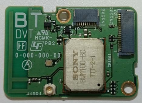
Click to zoom
Application Details
- Equipment Class
- DSS - Part 15 Spread Spectrum Transmitter
- Date of Grant
- Nov 03, 2015
- Application Purpose
- Original Equipment
- Date of Application
- Nov 03, 2015
- Equipment Note
- Bluetooth Module
- Frequency Range
- 2402.00000000 - 2480.00000000
- Company
- Sony Group Corporation
- Country
- Japan
Documents & Files
Document Text
Text extracted from the exhibit documents filed with the FCC. Open a document above to read the original.
Users Manual
Confidential Since this module is not sold to general end users directly, there is no user manual of module. For the details about this module, please refer to the specification sheet of module. This module should be installed in the host device according to the interface specification (installation procedure). 2. Regulatory information described in the manual of the end product 2.1. FCC This device complies with part 15 of the FCC Rules. Operation is subject to the following two conditions: (1) This device may not cause harmful interference, and (2) this device must accept any interference received, including interference that may cause undesired operation. FCC CAUTION Changes or modifications not expressly approved by the party responsible for compliance could void the user’s authority to operate the equipment. Note: This equipment has been tested and found to comply with the limits for a Class B digital device, pursuant to part 15 of the FCC Rules. These limits are designed to provide reasonable protection against harmful interference in a residential installation. This equipment generates, uses and can radiate radio frequency energy and, if not installed and used in accordance with the instructions, may cause harmful interference to radio communications. However, there is no guarantee that interference will not occur in a particular installation. If this equipment does cause harmful interference to radio or television reception, which can be determined by turning the equipment off and on, the user is encouraged to try to correct the interference by one or more of the following measures: —Reorient or relocate the receiving antenna. —Increase the separation between the equipment and receiver. —Connect the equipment into an outlet on a circuit different from that to which the receiver is connected. —Consult the dealer or an experienced radio/TV technician for help. This transmitter must not be co-located or operated in conjunction with any other antenna or transmitter. Confidential This equipment complies with FCC radiation exposure limits set forth for an uncontrolled environment and meets the FCC radio frequency (RF) Exposure Guidelines. This equipment has very low levels of RF energy that is deemed to comply without maximum permissive exposure evaluation (MPE). 2.2. IC This device complies with Industry Canada’s licence-exempt RSSs. Operation is subject to the following two conditions: (1) This device may not cause interference; and (2) This device must accept any interference, including interference that may cause undesired operation of the device. Le présent appareil est conforme aux CNR d’Industrie Canada applicables aux appareils radio exempts de licence. L’exploitation est autorisée aux deux conditions suivantes : 1) l’appareil ne doit pas produire de brouillage; 2) l’utilisateur de l’appareil doit accepter tout brouillage radioélectrique subi, même si le brouillage est susceptible d’en compromettre le fonctionnement. This equipment complies with IC radiation exposure limits set forth for an uncontrolled environment and meets RSS-102 of the IC radio frequency (RF) Exposure rules. This equipment has very low levels of RF energy that is deemed to comply without maximum permissive exposure evaluation (MPE). Cet équipement est conforme aux limites d’exposition aux rayonnements énoncées pour un environnement non contrôlé et respecte les règles d’exposition aux fréquences radioélectriques (RF) CNR-102 de l’IC. Cet équipement émet une énergie RF très faible qui est considérée comme conforme sans évaluation de l’exposition maximale autorisée (MPE). 3. Labelling 3.1. FCC FCC ID is printed on BT-LSP1 module as below. FCC ID: AK8BTLS1 If FCC ID on BT-LSP1 is not visible from outside of the end product, the product shall be labelled outside of it as below. Contains FCC ID: AK8BTLS1 3.2. IC IC number is printed on BT-LSP1 module as below. Confidential IC: 409B-BTLS1 If IC number on BT-LSP1 is not visible from outside of the end product, the product shall be labelled outside of it as below. Contains IC: 409B-BTLS1
Cover Letter(s)
Sony EMCS Corporation Letter of Authorization Date: October 16, 2015 UL Japan, Inc. 4383-326 Asama-cho, Ise-shi, Mie 516-0021 Japan FCC ID : AK8BTLS1 Applicant : Sony Corporation To whom it may concern: Please be advised we authorize Yoshihisa Maeda of Consumer Technology Division, UL Japan, Inc. to act on our behalf, until otherwise notified, for applications submitted for Federal Communication Commission Radio equipment applications submitted to UL Japan, Inc. We certify that we are not subject to denial of federal benefits, t hat includes FCC benefits, pursuant to Section 5301 of the Anti-Drug Abuse ACT of 1988, U.S.C. 862. Further, no party, as defined in 47 CFR 1.2002(b), to the application is subject to denial of federal benefits, that includes FCC benefits. The application for the subject equipment has not been submitted to another TCB for certification. Thank you for your attention to this matter. Sincerely, Hideo Nomura Sony EMCS Corporation
Cover Letter(s)
Sony EMCS Corporation Request for Limited Modular Transmitter Approval October 16, 2015 FCC ID : AK8BTLS1 Applicant : Sony Corporation This transmitter, model: BT-LSP1 is designed by us. It complies with the modular transmitters basic requirements (Item 1 to 8) in FCC Part 15 Subpart C Section 15.212 as indicated below: Modular Approval Checklist: Modular approval requirement Yes No (1) Have its own RF shielding. (2) Have buffered modulation/data inputs. (3) Have its own power supply regulation. This module does not have the power supply regulator. The stable voltage will be supplied by end product. Therefore end product will be required to have the power supply regulator. (4) Comply with the antenna and transmission system requirements of § 15.203, 15.204(b) and 15.204(c). (5) Tested in a stand-alone configuration. Unless the transmitter module will be battery powered, it must comply with the AC line conducted requirements found in FCC § 15.207. AC or DC power lines and data input/output lines connected to the module must not contain ferrites, unless they will be marketed with the module. The length of these lines shall be the length typical of actual use or, if that length is unknown, at least 10 centimeters to insure that there is no coupling between the case of the module and supporting equipment. Any accessories, peripherals, or support equipment connected to the module during testing shall be unmodified and commercially available. (6) Equipped with either a permanently affixed label or must be capable of electronically displaying its FCC ID. If the FCC ID is not visible when the module is installed inside another device, then the outside of the device into which the module is installed must also display a labe l referring to the enclosed module. (7) Comply with any specific rules or operating requirements that ordinarily apply to a complete transmitter and the manufacturer must provide adequate instructions along with the module to explain any such requirements. (8) Comply with any applicable RF exposure requirements in its final configuration: The modular transmitter complies with FCC radiation exposure requirement. Hideo Nomura Sony EMCS Corporation
Cover Letter(s)
Sony EMCS Corporation Request for Confidentiality Date: October 16, 2015 UL Japan, Inc. 4383-326 Asama-cho, Ise-shi, Mie 516-0021 Japan FCC ID : AK8BTLS1 Applicant : Sony Corporation To whom it may concern: Please be advised that the following information is to be held confidential on behalf of us, referring to the FCC rules 0.457 and 0.459: Block Diagram Theory of Operation Schematics The application contains technical information which we deem to be trade secrets and proprietary. If made public, the information might be used to the disadvantage of the applicant in the market place. Thank you for your attention to this matter. Sincerely, Hideo Nomura Sony EMCS Corporation
Cover Letter(s)
Sony EMCS Corporation Request for Short-Term Confidentiality Date: October 16, 2015 UL Japan, Inc. 4383-326 Asama-cho, Ise-shi, Mie 516-0021 Japan FCC ID : AK8BTLS1 Applicant : Sony Corporation To whom it may concern: Please be advised that the following information is to be held in confidence for 180 days from the date of the Grant of Equipment Authorization and behalf of us, referring to the FCC rules 0.457 and 0.459: External Photos Internal Photos Test Setup Photos User Manual The application contains technical information, which we deem to be trade secrets and proprietary. If made public, the information might be used to the disadvantage of the applicant in the market place. Thank you for your attention to this matter. Sincerely, ____________________________________ Hideo Nomura Sony EMCS Corporation
External Photos
Sony Corporation Photos Front With shield case Back Front Without shield case
ID Label/Location Info
Sony Corporation Label design and location
Internal Photos
Sony Corporation Photos Front With shield case Back Front Without shield case
RF Exposure Info
Sony EMCS Corporation RF Exposure / MPE Calculation No. : LIN-0521 Applicant : Sony Corporation Type of Equipment : Bluetooth Module Model No. : BT-LSP1 FCC ID : AK8BTLS1 Sony Corporation declares that Model: BT-LSP1 complies with FCC radiation exposure requirement specified in the FCC Rule 2.1091 (for mobile). RF Exposure Calculations: The following information provides the minimum separation distance for the highest gain antenna provided with the “BT-LSP1“ as calculated from (B) Limits for General Population / Uncontrolled Exposure of TABLE 1- LIMITS FOR MAXIMUM PERMISSIBLE EXPOSURE (MPE) of §1.1310 Radiofrequency radiation exposure limits. This calculation is based on the highest EIRP possible from the system, considering maximum power and antenna gain, and considering a 1mW/cm^2 uncontrolled exposure limit. The Friis formula used was: Where P = 2.16 mW (Maximum peak output power) G = 0.752 Numerical Antenna gain; equal to -1.24 dBi r = 20 cm (Separation distance) Power Density Result S = 0.000324 mW/cm2 Even taking into account the tolerance, this device can be satisfied with the limits.
Test Report
Project No: JB-Z0086-A Page 1 of 75 Sony EMCS EMC/RF Test Laboratory Main Lab. A2LA Cert. #3203.01 Kisarazu Site 8-4 Shiomi Kisarazu-shi, Chiba, 292-0834 Japan PHONE +81-(438) 37-2750 FAX +81-(438) 37-1021 RADIO TEST REPORT Project No. : JB-Z0086-A Client : Sony Corporation Address : 1-7-1 Konan, Minato-ku Tokyo 108-0075, Japan Type of Equipment : Bluetooth Module Model No. : BT-LSP1 Serial No. : 72, 84 FCC ID : AK8BTLS1 Regulation Applied : 47 CFR Part 15 Subpart C Final Judgment : Passed Sample Receipt : October 1, 2015 Testing : October 2, 2015 – October 7, 2015 Original Reported : October 14, 2015 Amend Reported : October 29, 2015 Amend: This report is to be replaced with the original report, Project No.JB-Z0086 because the test data is revised on . Voltage notation error correction 100V/50Hz ->120V/60Hz in the System configuration. Reported by : Approved Signatory : Takanori Oho Teruki Kurihara Test Engineer Technical Manager EMC/ RF Test Laboratory Main Lab. EMC/ RF Test Laboratory Main Lab. Design Technology Division Design Technology Division Sony EMCS Corporation Sony EMCS Corporation Notice * These test results relate only to the items (combination equipment, test configuration, operation condition etc.) tested. * This report shall not be reproduced except in full, without written approval of the laboratory. * This report must not be used by the client to claim product endorsement by A2LA or any agency of the U.S. Government. * All test results are traceable to the national and / or international standards. The testing in which “Non-accreditation” is displayed is outside the accreditation scopes in Sony EMCS EMC/ RF Test Laboratory. TESTING CERT #3203.01 Project No: JB-Z0086-A Page 2 of 75 Sony EMCS EMC/RF Test Laboratory Main Lab. A2LA Cert. #3203.01 Kisarazu Site 8-4 Shiomi Kisarazu-shi, Chiba, 292-0834 Japan PHONE +81-(438) 37-2750 FAX +81-(438) 37-1021 TABLE OF CONTENTS 1. General Information .................................................................................................................................................... 3 1.1. Description of Equipment Under Test (EUT) .................................................................................................................. 3 1.2. Summary of Test Result ...................................................................................................................................................... 4 1.3. Tested Methodology .............................................................................................................................................................. 5 1.4. Measurement Procedures .................................................................................................................................................... 5 1.5. Test Facility ............................................................................................................................................................................ 8 1.6. Uncertainty ............................................................................................................................................................................ 8 2. System Test Configuration .......................................................................................................................................... 9 2.1. Validation ............................................................................................................................................................................... 9 2.2. Test Operating Conditions ................................................................................................................................................... 9 2.3. Special Accessories ................................................................................................................................................................ 9 2.4. EUT Modifications ................................................................................................................................................................ 9 2.5. Configuration of Tested System ....................................................................................................................................... 10 3. Test Data ..................................................................................................................................................................... 12 3.1. AC Power-line Conducted Emissions ............................................................................................................................. 12 3.2. 20dB Bandwidth ................................................................................................................................................................. 13 3.3. Carrier Frequency Separation ......................................................................................................................................... 15 3.4. Number of Hopping Frequencies ..................................................................................................................................... 16 3.5. Time of Occupancy (Dwell Time) ..................................................................................................................................... 17 3.6. Maximum Peak Conducted Output Power ................................................................................................................... 20 3.7. Radiated Spurious Emissions .......................................................................................................................................... 21 3.8. Conducted Spurious Emissions for Band Edge............................................................................................................. 69 4. Method of Calculation ................................................................................................................................................ …
Text truncated - open the document above for the full version.
Test Setup Photos
Project No: JB-Z0086-A Page 73 of 75 Sony EMCS EMC/RF Test Laboratory Main Lab. A2LA Cert. #3203.01 Kisarazu Site 8-4 Shiomi Kisarazu-shi, Chiba, 292-0834 Japan PHONE +81-(438) 37-2750 FAX +81-(438) 37-1021 6. Photographs of test setup The following photographs show the arrangement of the worst case. 6.1. AC Power-line Conducted Emissions Measurement Photo(s) 6.2. Antenna-port Conducted Measurements Photo(s) Project No: JB-Z0086-A Page 74 of 75 Sony EMCS EMC/RF Test Laboratory Main Lab. A2LA Cert. #3203.01 Kisarazu Site 8-4 Shiomi Kisarazu-shi, Chiba, 292-0834 Japan PHONE +81-(438) 37-2750 FAX +81-(438) 37-1021 6.3. Radiated Spurious Emissions Measurement Photo(s) Below 30MHz 30 - 1000 MHz Above 1 GHz Project No: JB-Z0086-A Page 75 of 75 Sony EMCS EMC/RF Test Laboratory Main Lab. A2LA Cert. #3203.01 Kisarazu Site 8-4 Shiomi Kisarazu-shi, Chiba, 292-0834 Japan PHONE +81-(438) 37-2750 FAX +81-(438) 37-1021 < EUT position > X axis Y axis Z axis
Contact Information
Applicant
Kazuyuki Hori(Chief EMC/RF Compliance Specialist)
Technical Contact
Sony EMCS EMC/RF Test Laboratory Main Lab.Teruki Kurihara
[email protected]81-438-37-2750
Kisarazu Site 8-4 Shiomi Kisarazu-shi · Chiba · Japan
Test Firm
Sony GMOC EMC/RF Test Laboratory, Main LabTeruki Kurihara
Technical Specifications
| # | Rule Parts | Frequency Range | Power Output |
|---|---|---|---|
| 1 | 15C | 2.40 GHz - 2.48 GHz | 2.20 mW |
Other Applications from Sony Group Corporation
AK8WW81782
Aug 21, 2026Radio Equipment
Equipment Class
DSS - Part 15 Spread Spectrum TransmitterAK8CFIZCP2
Aug 03, 2026Wireless Controller
Equipment Class
DSS - Part 15 Spread Spectrum TransmitterAK8OEV321MUH
Apr 14, 2026LCD Monitor
Equipment Class
JAD - Part 15 Class A Digital DeviceAK8OEV431MUH
Apr 14, 2026LCD Monitor
Equipment Class
JAD - Part 15 Class A Digital DeviceAK8OEV271MUH
Apr 14, 2026LCD Monitor
Equipment Class
JAD - Part 15 Class A Digital Device