AK8ECM-W2BTRWireless Microphone
Sony Group Corporation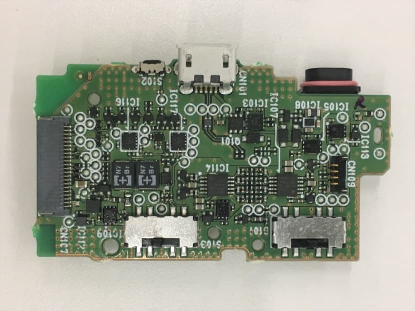
Click to zoom
Application Details
- Equipment Class
- DSS - Part 15 Spread Spectrum Transmitter
- Date of Grant
- Feb 07, 2021
- Application Purpose
- Original Equipment
- Date of Application
- Feb 07, 2021
- Equipment Note
- Wireless Microphone
- Frequency Range
- 2402.00000000 - 2480.00000000
- Company
- Sony Group Corporation
- Country
- Japan
Documents & Files
Document Text
Text extracted from the exhibit documents filed with the FCC. Open a document above to read the original.
Users Manual
5-025-980-01(1)5-025-980-01(1)5-025-980-01(1) To prevent accidentally swallowing of the device parts, do not put them in your mouth. To store this unit, avoid any locations subject to extremely high/low temperatures, high humidity, or direct sunlight. Notice This product has been tested and found compliant with the limits set out in the EMC regulation for using connection cables shorter than 3 meters (9.8 feet) except LAN cable. Note on Use of Wireless Function Use of the wireless function of the unit may not be permitted, depending on the rules and regulations of the country or region. Always observe the rules and regulations of the country or region regarding use. When using this unit in an aircraft or a hospital, follow the instructions from the airline company or the hospital to avoid possible interference with instruments or medical devices caused by radio waves from this unit. For Customers in the U.S.A. and Canada RECYCLING RECHARGEABLE BATTERIES Rechargeable batteries are recyclable. You can help preserve our environment by returning your used rechargeable batteries to the collection and recycling location nearest you. For more information regarding recycling of rechargeable batteries, visit www.sony.com/electronics/eco/environmental- management The available scientific evidence does not show that any health problems are associated with using low power wireless devices. There is no proof, however, that these low power wireless devices are absolutely safe. Low power Wireless devices emit low levels of radio frequency energy (RF) in the microwave range while being used. Whereas high levels of RF can produce health effects (by heating tissue), exposure of low-level RF that does not produce heating effects causes no known adverse health effects. Many studies of low-level RF exposures have not found any biological effects. Some studies have suggested that some biological effects might occur, but such findings have not been confirmed by additional research. This equipment has been tested and found to comply with FCC/ISED radiation exposure limits set forth for an uncontrolled environment and meets the FCC radio frequency (RF) Exposure Guidelines and RSS-102 of the ISED radio frequency (RF) Exposure rules. For Customers in the U.S.A. CAUTION You are cautioned that any changes or modifications not expressly approved in this manual could void your authority to operate this equipment. Note: This equipment has been tested and found to comply with the limits for a Class B digital device, pursuant to Part 15 of the FCC Rules. These limits are designed to provide reasonable protection against harmful interference in a residential installation. This equipment generates, uses, and can radiate radio frequency energy and, if not installed and used in accordance with the instructions, may cause harmful interference to radio communications. However, there is no guarantee that interference will not occur in a particular installation. If this equipment does cause harmful interference to radio or television reception, which can be determined by turning the equipment off and on, the user is encouraged to try to correct the interference by one or more of the following measures: • Reorient or relocate the receiving antenna. • Increase the separation between the equipment and receiver. •Connect the equipment into an outlet on a circuit different from that to which the receiver is connected. •Consult the dealer or an experienced radio/TV technician for help. This equipment must not be co-located or operated in conjunction with any other antenna or transmitter. For Customers in Canada This device contains licence-exempt transmitter(s)/ receiver(s) that comply with Innovation, Science and Economic Development Canada’s licence-exempt RSS(s). Operation is subject to the following two conditions: (1) This devic e may not cause interference. (2) This device must accept any interference, including interference that may cause undesired operation of the device. For Customers in Europe Manufacturer: Sony Corporation EU Importer/manufacturer’s authorized representative: Sony Europe B.V., Da Vincilaan 7-D1, 1930 Zaventem, Belgium. UK Importer/manufacturer’s authorized representative: Sony Europe B.V., The Heights, Brooklands, Weybridge, Surrey KT13 0XW, United Kingdom. Hereby, Sony Corporation declares that this equipment is in compliance Directive 2014/53/EU. The full text of the EU declaration of conformity is available at the following internet address: https://compliance.sony.eu Hereby, Sony Corporation declares that this equipment is in compliance with the UK relevant statutory requirements. The full text of the declaration of conformity is available at the following internet address: https://compliance.sony.co.uk Disposal of waste batteries and electrical and electronic equipment (applicable in the European Union and other countries with separate collection systems) This symbol on the product, the battery or on the packaging indicates that the product and the battery shall not be treated as household waste. On certain batteries this symbol might be used in combination with a chemical symbol. The chemical symbol for lead (Pb) is added if the battery contains more than 0.004% lead. By ensuring that these products and batteries are disposed of correctly, you will help to prevent potentially negative consequences for the environment and human health which could be caused by inappropriate waste handling. The recycling of the materials will help to conserve natural resources. In case of products that for safety, performance or data integrity reasons require a permanent connection with an incorporated battery, this battery should be replaced by qualified service staff only. To ensure that the battery and the electrical and electronic equipment will be treated properly, hand over these products at end-of-life to the appropriate collection point for the recycling of electrical and electronic equipment. For all other batte…
Text truncated - open the document above for the full version.
Users Manual
ECM-W2BT 5-024-898-01(1)ECM-W2BT 5-024-898-01(1)ECM-W2BT 5-024-898-01(1)ECM-W2BT 5-024-898-01(1) • 火災、感電の原因となることがありますので以下にご注意ください。 ‒ 分解や改造をしない ‒ ぬれた手で使用しない ‒ 内部に水や異物(金属類や燃えやすい物など)を入れない ‒ 水滴のかかる場所など湿気の多い場所やほこり、油煙、湯気の多い 場所では使わない • 破損や不具合の原因となる場合がありますので以下にご注意くだ さい。 ‒ 本機は精密機器のため、落としたり、たたいたり、強い衝撃を与え ない ‒ 端子部を直接手で触らない ‒ 高温多湿の場所での使用、保存を避ける • 内部点検や修理は相談窓口にご依頼ください。 • 落としたり、液体がかかったりしないように丁寧に扱ってください。 • 本機は防じん、防滴性に配慮して設計されていますが、防水性能は備 えていません。雨中での使用時は、本機に雨がかからないようにして ください。 • カメラの内蔵フラッシュをお使いの場合は、レシーバーを取り外し てください。 • マイクロホンの機銘板はクリップの下にあります。 • 録音中はカメラやレンズの作動音、操作音などが記録されてしまう ことがあります。録音中に本機に触れると、ノイズとして録音されて しまいます。 • 運転中は使用しないでください。 自動車、オートバイなどの運転をしながらヘッドホンやイヤホンな どを使用したり、細かい操作をすることは絶対におやめください。 交通事故の原因となります。 また、歩きながら使用するときも、事故を防ぐため、周囲の交通や路 面状況に充分にご注意ください。 機器に内蔵されている充電式電池はリサイクル 出来ます。 この充電式電池の取り外しはお客様ご自身では 行わず、ソニーの相談窓口にご相談ください 各部名称 レ シ ー バ ー( イ ラ ス ト -(1)参照) 1 スライドスイッチ(MIC OUT ANALOG/電源OFF/DIGITAL) 2 モードスイッチ(RCVR/MIX/MIC) 3 マルチインターフェースフット 4 電源ランプ(緑:電源ON、オレンジ:充電中) 5 LINKランプ 6 内蔵マイク 7 マイクロUSB端子 8 マイク出力端子 9 端子保護ホルダー マ イ ク ロ ホ ン( イ ラ ス ト -(2)参照) 10 LINKランプ 11 電源ランプ(緑:電源ON、オレンジ:充電中) 12 内蔵マイク 13 外部マイク入力端子 14 電源スイッチ 15 ATTスイッチ 16 マイクロUSB端子 17 クリップ 18 ウインドスクリーン 主な仕様 通信仕様 通信方式Bluetooth標準規格 Ver. 5.0 出力Bluetooth標準規格 Power Class 1 主なBluetooth プロファイル Advanced A udio Dis tribution P rofile 通信距離*最大 200 m * マイクロホンを立てて、レシーバーを真っ直ぐに向かい合わせたと きの目安となる距離です。 金属、人体などの障害物や反射面の有無など周囲の状況や電波状況 により変化します。 レシーバー マイク方式モノラル 無指向性 外形寸法(約)34 mm × 28.7 mm × 53 mm (幅/高さ/奥行き) 質量(約)28 g マイクロホン(トランスミッター) マイク方式モノラル 無指向性 外形寸法(約) 3 0.6 mm × 67.6 mm × 19 mm (幅/高さ/奥行き) 質量(約)27 g 同梱物 レシーバー(ECM-W2BT(R))(1)、マイクロホン(トランスミッター) (ECM-W2BT(T))(1)、ウインドスクリーン(1)、ポーチ(1)、 録音ケーブル(1)、マイクロUSBケーブル(1)、端子保護ホルダー(1)、 印刷物一式 仕様および外観は、改良のため予告なく変更することがありますが、 ご了承ください。 • Bluetooth®ワードマークおよびロゴは、Bluetooth S IG, In c.が所有 する登録商標であり、ソニー株式会社はこれらのマークをライセン スに基づいて使用しています。 • Multi I nterface Sho e(マルチインターフェースシュー)はソニー株 式会社の商標です。 保証書とアフターサービス 保証書 • この製品には保証書が添付されていますので、お買い上げの際、お受 け取りください。 • 所定事項の記入および記載内容をお確かめのうえ、大切に保管して ください。 • 保証期間は、お買い上げ日より1年間です。 アフターサービス 調子が悪いときはまずチェックを ヘルプガイドなどを参考にして故障かどうかお調べください。 それでも具合の悪いときは ソニーの相談窓口にご相談ください。 保証期間中の修理は 保証書の記載内容に基づいて修理させていただきます。詳しくは保証 書をご覧ください。 保証期間経過後の修理は 修理によって機能が維持できる場合は、ご要望により有料修理させて いただきます。 部品の保有期間について 当社では本機の補修用性能部品(製品の機能を維持するために必要な 部品)を、製造打ち切り後最低7年間保有しています。ただし、故障の状 況その他の事情により、修理に代えて製品交換をする場合があります のでご了承ください。保有期間が経過したあとも、故障箇所によって は修理可能の場合がありますので、お買い上げ店か、ソニーの相談窓 口にご相談ください。 ご相談になるときは次のことをお知らせください。 • 型名:ECM-W2BT(レシーバー単体 ECM-W2BT(R)、 マイクロホン単体 ECM-W2BT(T)) • 故障の状態:できるだけ詳しく • お買い上げ年月日 「402」+「#」 About the manual for this product For details on using the product, refer to the “Help Guide” (web manual). “Help Guide” (Web manual) https://rd1.sony.net/help/ilc/2080/h_zz/ For Customers in the U.S.A. For question regarding your product or for the Sony Service Center nearest you, call 1-800-222-SONY (7669) . Supplier’s Declaration of Conformity Trade Name : SONY Model : ECM-W2BT(T)/ ECM-W2BT(R) Responsible Party : Sony Electronics Inc. Address : 16535 Via Esprillo, San Diego, CA 92127 U.S.A. Telephone Number : 858-942-2230 This device complies with part 15 of the FCC rules. Operation is subject to the following two conditions: (1) This device may not cause harmful interference, and (2) This device must accept any interference received, including interference that may cause undesired operation. Notes on use The Wireless Microphone ECM-W2BT (referred to below as “this unit”) is compatible with a camera that has a Multi Interface Shoe such as a Sony Interchangeable Lens Digital Camera (referred to below as “camera”). Even if your camera has a Multi Interface Shoe, you may be unable to use it with this unit or some functions may not work. • This unit uses Bluetooth wireless communication technology. • See the operating instructions of this unit and refer to the operating instructions of your camera. • For camera models compatible with this unit, visit the website at: https://www.sony.net/dics/w2bt/ • To avoid the risk of a fire or an electric shock, observe the following: – Do not disassemble or alter this unit. – Do not use this unit with wet hands. – Do not allow ingress of water or foreign matters (metal, flammable substances, etc.) to this unit. – Do not use this unit in a place subject to water splashes, high humidity, dust, oil fumes, and steam. • To avoid the risk of damage or a malfunction, observe the following: – This unit is precision equipment. Do not drop the unit, hit it, or subject it to a strong physical impact. – Do not touch the electrical contacts on this unit with bare hands. – Do not use or store this unit in a place subject to high temperatures and humidity. • For interior inspection and repair of this unit, contact your Sony dealer or local authorized Sony service facility. • Handle this unit with care to avoid the risk of dropping it or letting it exposed to liquid. • This unit is designed to be dust and moisture-resistant, but is not waterproof or splash-proof. When you use the unit in rainy conditions, do not let the unit get wet. • To use the built-in flash of the camera, remove the receiver of this unit from the camera. • The nameplate is under the clip of the microphone. • While recording is in progress, operation and handling noises of a camera or a lens may be recorded. Touching this unit while recording is in progress causes a noise to be included in the recording. • Do not use this unit while driving a vehicle. While driving a vehicle, such as a car or a motorcycle, do not use headphones, earphones, or the like, nor do you perform fine operations to avoid a traffic accident. In addition, when you use this unit while walking, always pay attention to the surrounding traffic and the road surface conditions to avoid an accident. Identifying the parts Receiver (see illustration -(1)) 1 Slide switch (MIC OUT ANALOG/Power OFF/DIGITAL) 2 Mode switch (RCVR/MIX/MIC) 3 Multi Interface foot 4 Power lamp (Green: Powered, Orange: Charging the battery) 5 LINK lamp 6 Internal microphone 7 Micro USB terminal 8 Microphone out jack 9 Connector p…
Text truncated - open the document above for the full version.
Cover Letter(s)
Date: January 18, 2021 UL Verification Services Inc. 47173 Benicia Street, Fremont, CA 94538 Applicant: Sony Corporation FCC ID: AK8ECM-W2BTR To whom it may concern: We, the undersigned, hereby authorize Akiko Nishimura of Consumer Technology Division, UL Japan, Inc. to act on our behalf in all manners relating to application for equipment authorization, including signing of all documents relating to these matters. Any and all acts carried out by UL Japan, Inc. on our behalf shall have the same effect as acts of our own. We, the undersigned, hereby certify that we are not subject to a denial of federal benefits, that includes FCC benefits, pursuant to Section 5301 of the Anti-Drug Abuse Act of 1988, 21 U.S.C. 862. This authorization is valid until further written notice from the applicant. The application for the subject equipment has not been submitted to another TCB for certification. Sincerely, Hideo Nomura Sony Global Manufacturing & Operations Corporation
Cover Letter(s)
Request for Confidentiality Date: January 18, 2021 UL Verification Services Inc. 47173 Benicia Street, Fremont, CA 94538 Applicant : Sony Corporation FCC ID : AK8ECM-W2BTR To whom it may concern: Please be advised that the following information is to be held confidential on behalf of us, referring to the FCC rules 0.457 and 0.459: Block Diagram Theory of Operation Schematics The application contains technical information which we deem to be trade secrets and proprietary. If made public, the information might be used to the disadvantage of the applicant in the market place. Thank you for your attention to this matter. Sincerely, Sincerely, Hideo Nomura Sony Global Manufacturing & Operations Corporation
Cover Letter(s)
Request for Short-Term Confidentiality Date: January 18, 2021 UL Verification Services Inc. 47173 Benicia Street, Fremont, CA 94538 FCC ID : AK8ECM-W2BTR Applicant : Sony Corporation To whom it may concern: Please be advised that the following information is to be held in confidence until February 28, 2021 from the date of the Grant of Equipment Authorization and behalf of us, referring to the FCC rules 0.457 and 0.459: External Photos Internal Photos Test Setup Photos User Manual The application contains technical information, which we deem to be trade secrets and proprietary. If made public, the information might be used to the disadvantage of the applicant in the market place. Thank you for your attention to this matter. Sincerely, ____________________________________ Hideo Nomura Sony Global Manufacturing & Operations Corporation Sony Global Manufacturing & Operations Corporation
Cover Letter(s)
Sony Corporation Special Power of Attorney I, Kazuyuki Hori of Sony Corporation, hereby appoint Hideo Nomura of Sony Global Manufacturing & Operations Corporation to represent me to act on my behalf to do any and all of the following. Sign on my behalf the agency, anti-drug and confidentiality cover letters and apply to FCC for the products. The rights, powers and authority in fact to exercise any and all of the rights and powers herein granted shall Manufacturing & commence and be in full force from December 1, 2020 and continue to be effective unless specifically terminated by either party. Dated December 1, 2020 Kazuyuki Hori Company: Sony Corporation Country: Japan
External Photos
ECM-W2BT ProductPicture Right View Left View Back View Bottom View Top View ECM-W2BT(R)
ID Label/Location Info
Label Location ECM-W2BT(R) 1.41mm
Internal Photos
ECM-W2BT(R) Receiver Unit Main PWB TB0012611 Sub PWB( Mic element) inner side outer side Main PWB surface Main PWB back-side Sub PWB Pattern layout of RF signal line ECM-W2BT(R) FPC Antenna (TG0002811) Bluetooth System LSI Front End Amp. AntennaContact Main PWB TB0012611 FPC Antenna (TG0002811) Position/Photo of Antenna ECM-W2BT(R) FPC Antenna (TG0002811)
RF Exposure Info
Project No: JB-Z0791-B Model No.: ECM-W2BT(R) FCC ID: AK8ECM-W2BTR Issued: February 5, 2021 Page 1 of 60 Sony Global Manufacturing & Operations Corporation EMC/RF Test Laboratory, Main Lab. 8-4 Shiomi Kisarazu-shi Chiba-ken, 292-0834, Japan PHONE +81 438 37 2750 FAX +81 438 37 1021 SAR TEST REPORT Project No. : JB-Z0791-B Client : Sony Corporation Address : 1-7-1 Konan Minato-ku Tokyo, 108-0075 Japan Type of Equipment : Wireless Microphone Model No. : ECM-W2BT(R) FCC ID : AK8ECM-W2BTR Regulation Applied : FCC 47 CFR 2.1093 SAR Limits : Exposure Characteristics Spatial Peak SAR (Head and Trunk) averaged over any 1 g of tissue General Public Exposure 1.6 W/kg The Highest Reported SAR : RF Exposure Conditions Equipment Class Note(s) DSS/DTS Bluetooth Body-Worn 0.242 W/kg Test Result : Complied Sample Receipt : September 17, 2020 Testing : September 18, 2020 (for conducted power measurements) November 13, 2020 (for SAR measurements) Reported : February 5, 2021 Reported by : Approved Signatory : Hisae Takayama Takashi Yamada Test Engineer Technical Manager EMC/ RF Test Laboratory Main Lab. EMC/ RF Test Laboratory Main Lab. Design Technology Division Design Technology Division Sony Global Manufacturing & Operations Corporation Sony Global Manufacturing & Operations Corporation Notice * These test results relate only to the items (combination equipment, test configuration, operation condition etc.) tested. * This report shall not be reproduced except in full, without written approval of the laboratory. * This report must not be used by the client to claim product endorsement by A2LA or any agency of the U.S. Government. * All test results are traceable to the national and / or international standards. * The testing in which “Non-accreditation” is displayed is outside the accreditation scopes in Sony Global Manufacturing & Operations Corporation EMC/ RF Test Laboratory. * This report replaces and supersedes all previous versions. Refer to Revision History on the following page. TESTING CERT #3203.01 Format No.: NV1-1-01 Version 5.0 Project No: JB-Z0791-B Model No.: ECM-W2BT(R) FCC ID: AK8ECM-W2BTR Issued: February 5, 2021 Page 2 of 60 Sony Global Manufacturing & Operations Corporation EMC/RF Test Laboratory, Main Lab. 8-4 Shiomi Kisarazu-shi Chiba-ken, 292-0834, Japan PHONE +81 438 37 2750 FAX +81 438 37 1021 REVISION HISTORY Project No. Revision Page Description Issued date JB-Z0791 Original - - December 14, 2020 JB-Z0791-A 1 1,4 Corrected the FCC ID. January 19, 2021 JB-Z0791-B 2 28,29 Updated the reported SAR according to the specification change of the maximum duty cycle of the DUT specified by the client. February 5, 2021 DISCLAIMER This report includes the information provided by the customer as below; - Cover page : Client and product related information - Clause 1.1 : Description of Device Under Test (DUT) - Clause 1.2 : Antenna Placement - Clause 1.3 : Simultaneous Transmission Conditions - Clause 1.4 : Nominal and Maximum Possible Power (Maximum Tune-up Tolerance Limit) * The laboratory is not responsible for results affected by the above information. Project No: JB-Z0791-B Model No.: ECM-W2BT(R) FCC ID: AK8ECM-W2BTR Issued: February 5, 2021 Page 3 of 60 Sony Global Manufacturing & Operations Corporation EMC/RF Test Laboratory, Main Lab. 8-4 Shiomi Kisarazu-shi Chiba-ken, 292-0834, Japan PHONE +81 438 37 2750 FAX +81 438 37 1021 TABLE OF CONTENTS 1. General Information .................................................................................................................................... 4 1.1. Description of Device Under Test (DUT) ............................................................................................. 4 1.2. Antenna Placement ................................................................................................................................ 4 1.3. Nominal and Maximum Possible Power (Maximum Tune-up Tolerance Limit) .......................... 5 1.4. RF Exposure Conditions ........................................................................................................................ 5 1.5. RF Exposure Limits ................................................................................................................................ 5 1.6. SAR Test Exclusion ................................................................................................................................ 6 1.7. Test Specification, Methods and Procedures ....................................................................................... 7 1.8. Test Facilities and Accreditation .......................................................................................................... 8 2. Test Set-up .................................................................................................................................................... 9 2.1. Test Equipment and Measurement Software Lists ........................................................................... 9 2.2. Measurement System Description ..................................................................................................... 11 2.3. Measurement System Main Components ......................................................................................... 12 2.4. Tissue Simulating Liquids ................................................................................................................... 15 2.5. SAR Measurement ............................................................................................................................... 16 2.6. Measurement Uncertainty .................................................................................................................. 17 2.7. Dielectric Parameter Measurement of Tissue Simulating Liquids ............................................... 20 2.8. System Check Measurement .............................................................................................................. 22 3. Cond…
Text truncated - open the document above for the full version.
RF Exposure Info
Project No: JB-Z0791-B Model No.: ECM-W2BT(R) FCC ID: AK8ECM-W2BTR Issued: February 5, 2021 Page 34 of 60 Sony Global Manufacturing & Operations Corporation EMC/RF Test Laboratory, Main Lab. 8-4 Shiomi Kisarazu-shi Chiba-ken, 292-0834, Japan PHONE +81 438 37 2750 FAX +81 438 37 1021 Appendix C. Calibration Certificate C.1. E-Field Probe EX3DV4 (Serial No. 3921 / Control No. WA0002) Please see the following pages. Project No: JB-Z0791-B Model No.: ECM-W2BT(R) FCC ID: AK8ECM-W2BTR Issued: February 5, 2021 Page 35 of 60 Sony Global Manufacturing & Operations Corporation EMC/RF Test Laboratory, Main Lab. 8-4 Shiomi Kisarazu-shi Chiba-ken, 292-0834, Japan PHONE +81 438 37 2750 FAX +81 438 37 1021 Project No: JB-Z0791-B Model No.: ECM-W2BT(R) FCC ID: AK8ECM-W2BTR Issued: February 5, 2021 Page 36 of 60 Sony Global Manufacturing & Operations Corporation EMC/RF Test Laboratory, Main Lab. 8-4 Shiomi Kisarazu-shi Chiba-ken, 292-0834, Japan PHONE +81 438 37 2750 FAX +81 438 37 1021 Project No: JB-Z0791-B Model No.: ECM-W2BT(R) FCC ID: AK8ECM-W2BTR Issued: February 5, 2021 Page 37 of 60 Sony Global Manufacturing & Operations Corporation EMC/RF Test Laboratory, Main Lab. 8-4 Shiomi Kisarazu-shi Chiba-ken, 292-0834, Japan PHONE +81 438 37 2750 FAX +81 438 37 1021 Project No: JB-Z0791-B Model No.: ECM-W2BT(R) FCC ID: AK8ECM-W2BTR Issued: February 5, 2021 Page 38 of 60 Sony Global Manufacturing & Operations Corporation EMC/RF Test Laboratory, Main Lab. 8-4 Shiomi Kisarazu-shi Chiba-ken, 292-0834, Japan PHONE +81 438 37 2750 FAX +81 438 37 1021 Project No: JB-Z0791-B Model No.: ECM-W2BT(R) FCC ID: AK8ECM-W2BTR Issued: February 5, 2021 Page 39 of 60 Sony Global Manufacturing & Operations Corporation EMC/RF Test Laboratory, Main Lab. 8-4 Shiomi Kisarazu-shi Chiba-ken, 292-0834, Japan PHONE +81 438 37 2750 FAX +81 438 37 1021 Project No: JB-Z0791-B Model No.: ECM-W2BT(R) FCC ID: AK8ECM-W2BTR Issued: February 5, 2021 Page 40 of 60 Sony Global Manufacturing & Operations Corporation EMC/RF Test Laboratory, Main Lab. 8-4 Shiomi Kisarazu-shi Chiba-ken, 292-0834, Japan PHONE +81 438 37 2750 FAX +81 438 37 1021 Project No: JB-Z0791-B Model No.: ECM-W2BT(R) FCC ID: AK8ECM-W2BTR Issued: February 5, 2021 Page 41 of 60 Sony Global Manufacturing & Operations Corporation EMC/RF Test Laboratory, Main Lab. 8-4 Shiomi Kisarazu-shi Chiba-ken, 292-0834, Japan PHONE +81 438 37 2750 FAX +81 438 37 1021 Project No: JB-Z0791-B Model No.: ECM-W2BT(R) FCC ID: AK8ECM-W2BTR Issued: February 5, 2021 Page 42 of 60 Sony Global Manufacturing & Operations Corporation EMC/RF Test Laboratory, Main Lab. 8-4 Shiomi Kisarazu-shi Chiba-ken, 292-0834, Japan PHONE +81 438 37 2750 FAX +81 438 37 1021 Project No: JB-Z0791-B Model No.: ECM-W2BT(R) FCC ID: AK8ECM-W2BTR Issued: February 5, 2021 Page 43 of 60 Sony Global Manufacturing & Operations Corporation EMC/RF Test Laboratory, Main Lab. 8-4 Shiomi Kisarazu-shi Chiba-ken, 292-0834, Japan PHONE +81 438 37 2750 FAX +81 438 37 1021 Project No: JB-Z0791-B Model No.: ECM-W2BT(R) FCC ID: AK8ECM-W2BTR Issued: February 5, 2021 Page 44 of 60 Sony Global Manufacturing & Operations Corporation EMC/RF Test Laboratory, Main Lab. 8-4 Shiomi Kisarazu-shi Chiba-ken, 292-0834, Japan PHONE +81 438 37 2750 FAX +81 438 37 1021 Project No: JB-Z0791-B Model No.: ECM-W2BT(R) FCC ID: AK8ECM-W2BTR Issued: February 5, 2021 Page 45 of 60 Sony Global Manufacturing & Operations Corporation EMC/RF Test Laboratory, Main Lab. 8-4 Shiomi Kisarazu-shi Chiba-ken, 292-0834, Japan PHONE +81 438 37 2750 FAX +81 438 37 1021 C.2. System Validation Dipole D2450V2 (Serial No. 936 / Control No. WA0026) Please see the following pages. Project No: JB-Z0791-B Model No.: ECM-W2BT(R) FCC ID: AK8ECM-W2BTR Issued: February 5, 2021 Page 46 of 60 Sony Global Manufacturing & Operations Corporation EMC/RF Test Laboratory, Main Lab. 8-4 Shiomi Kisarazu-shi Chiba-ken, 292-0834, Japan PHONE +81 438 37 2750 FAX +81 438 37 1021 Project No: JB-Z0791-B Model No.: ECM-W2BT(R) FCC ID: AK8ECM-W2BTR Issued: February 5, 2021 Page 47 of 60 Sony Global Manufacturing & Operations Corporation EMC/RF Test Laboratory, Main Lab. 8-4 Shiomi Kisarazu-shi Chiba-ken, 292-0834, Japan PHONE +81 438 37 2750 FAX +81 438 37 1021 Project No: JB-Z0791-B Model No.: ECM-W2BT(R) FCC ID: AK8ECM-W2BTR Issued: February 5, 2021 Page 48 of 60 Sony Global Manufacturing & Operations Corporation EMC/RF Test Laboratory, Main Lab. 8-4 Shiomi Kisarazu-shi Chiba-ken, 292-0834, Japan PHONE +81 438 37 2750 FAX +81 438 37 1021 Project No: JB-Z0791-B Model No.: ECM-W2BT(R) FCC ID: AK8ECM-W2BTR Issued: February 5, 2021 Page 49 of 60 Sony Global Manufacturing & Operations Corporation EMC/RF Test Laboratory, Main Lab. 8-4 Shiomi Kisarazu-shi Chiba-ken, 292-0834, Japan PHONE +81 438 37 2750 FAX +81 438 37 1021 Project No: JB-Z0791-B Model No.: ECM-W2BT(R) FCC ID: AK8ECM-W2BTR Issued: February 5, 2021 Page 50 of 60 Sony Global Manufacturing & Operations Corporation EMC/RF Test Laboratory, Main Lab. 8-4 Shiomi Kisarazu-shi Chiba-ken, 292-0834, Japan PHONE +81 438 37 2750 FAX +81 438 37 1021 Project No: JB-Z0791-B Model No.: ECM-W2BT(R) FCC ID: AK8ECM-W2BTR Issued: February 5, 2021 Page 51 of 60 Sony Global Manufacturing & Operations Corporation EMC/RF Test Laboratory, Main Lab. 8-4 Shiomi Kisarazu-shi Chiba-ken, 292-0834, Japan PHONE +81 438 37 2750 FAX +81 438 37 1021 Project No: JB-Z0791-B Model No.: ECM-W2BT(R) FCC ID: AK8ECM-W2BTR Issued: February 5, 2021 Page 52 of 60 Sony Global Manufacturing & Operations Corporation EMC/RF Test Laboratory, Main Lab. 8-4 Shiomi Kisarazu-shi Chiba-ken, 292-0834, Japan PHONE +81 438 37 2750 FAX +81 438 37 1021 Project No: JB-Z0791-B Model No.: ECM-W2BT(R) FCC ID: AK8ECM-W2BTR Issued: February 5, 2021 Page 53 of 60 Sony Global Manufacturing & Operations Corporation EMC/RF Test Laboratory, Main Lab. 8-4 Shiomi Kisarazu-shi Chiba-ken, 292-0834, Japan PHONE +81 438 37 2750 FAX +81 438 37 1021
Test Report
Project No: JB-Z0788-B Page 1 of 26 Sony Global Manufacturing & Operations Corporation EMC/RF Test Laboratory, Main Lab. 8-4 Shiomi Kisarazu-shi Chiba-ken, 292-0834, Japan PHONE +81 438 37 2750 FAX +81 438 37 1021 RADIO TEST REPORT (for Bluetooth classic) Project No. : JB-Z0788-B Client : Sony Corporation Client’s Address : 1-7-1 Konan Minato-ku Tokyo, 108-0075 Japan Product Name : Wireless Microphone Model No. : ECM-W2BT(R) FCC ID : AK8ECM-W2BTR Te s t S t a n d a r d : 47 CFR Part 15 Subpart C Sample Receipt Date : October 20, 2020 Te s t D a t e : November 5, 2020 to November 19, 2020 Report Date : January 25, 2021 Test Result : Complied Notice : * These test results relate only to the items (combination equipment, test configuration, operation condition etc.) tested. * This report shall not be reproduced except in full, without written approval of the laboratory. * This report must not be used by the client to claim product endorsement by A2LA or any agency of the U.S. * Hereby certify that no party is subject to a denial of federal benefits pursuant to section 5301 of the Anti-Drug Abuse Act. * All test results are traceable to the national and / or international standards. * The testing in which “Non-accreditation” is displayed is outside the accreditation scopes in Sony Global Manufacturing & Operations Corporation EMC/ RF Test Laboratory. * This report replaces and supersedes all previous versions. Refer to Revision History on the following page. Reported by: Takanori Oho Technical Manager EMC/RF Test Laboratory, Main Lab. Design Technology Division Approved Signatory: Takashi Yamada Technical Manager EMC/RF Test Laboratory, Main Lab. Design Technology Division Format No.: NV1-1-01 Version 5.0 TESTING CERT #3203.01 Project No: JB-Z0788-B Page 2 of 26 Sony Global Manufacturing & Operations Corporation EMC/RF Test Laboratory, Main Lab. 8-4 Shiomi Kisarazu-shi Chiba-ken, 292-0834, Japan PHONE +81 438 37 2750 FAX +81 438 37 1021 TABLE OF CONTENTS 1. General Information ................................................................................................................................................. 3 1.1. Description of Equipment Under Test (EUT) ...................................................................................................... 3 1.2. Summary of Test Result ..........…
Text truncated - open the document above for the full version.
Contact Information
Applicant
Kazuyuki Hori(Chief EMC/RF Compliance Specialist)
Technical Contact
Sony Global Manufacturing & Operations CorporationTakashi Yamada
[email protected]81-438-37-2750
8-4 Shiomi Kisarazu-shi · Chiba-ken · Japan
Test Firm
Sony GMOC EMC/RF Test Laboratory, Main LabTeruki Kurihara
Technical Specifications
| # | Rule Parts | Frequency Range | Power Output |
|---|---|---|---|
| 1 | 15C | 2.40 GHz - 2.48 GHz | 21.20 mW |
Other Applications from Sony Group Corporation
AK8WW81782
Aug 21, 2026Radio Equipment
Equipment Class
DSS - Part 15 Spread Spectrum TransmitterAK8CFIZCP2
Aug 03, 2026Wireless Controller
Equipment Class
DSS - Part 15 Spread Spectrum TransmitterAK8OEV321MUH
Apr 14, 2026LCD Monitor
Equipment Class
JAD - Part 15 Class A Digital DeviceAK8OEV431MUH
Apr 14, 2026LCD Monitor
Equipment Class
JAD - Part 15 Class A Digital DeviceAK8OEV271MUH
Apr 14, 2026LCD Monitor
Equipment Class
JAD - Part 15 Class A Digital Device