AK8M19DFR1Wireless communication module
Sony Group Corporation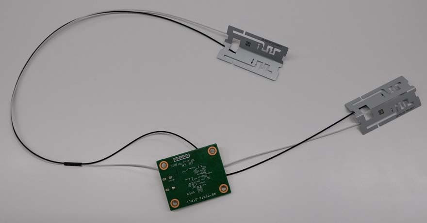
Click to zoom
Application Details
- Equipment Class
- NII - Unlicensed National Information Infrastructure TX
- Date of Grant
- Jun 20, 2020
- Application Purpose
- Original Equipment
- Date of Application
- Jun 20, 2020
- Equipment Note
- Wireless communication module
- Frequency Range
- 5745.00000000 - 5825.00000000
- Company
- Sony Group Corporation
- Country
- Japan
Documents & Files
Document Text
Text extracted from the exhibit documents filed with the FCC. Open a document above to read the original.
Users Manual
User Manual Since this module is not sold to general end users directly, there is no user manual of module. For the details about this module, please refer to the specification sheet of module. This module should be installed in the host device according to the interface specification (installation procedure).
Cover Letter(s)
1 KDB996369 Check List FCC ID: AK8M19DFR1 Applicant: Sony Corporation This transmitter complies with KDB996369 D03 as indicated below: Modular approval requirement Applicable Not Applicable 2.2 List of applicable FCC rules List the FCC rules that are applicable to the modular transmitter. These are the rules that specifically establish the bands of operation, the power, spurious emissions, and operating fundamental frequencies. DO NOT list compliance to unintentional-radiator rules (Part 15 Subpart B) since that is not a condition of a module grant that is extended to a host manufacturer. See also Section 2.10 below concerning the need to notify host manufacturers that further testing is required. Please refer to Interface Specification. 2.3 Summarize the specific operational use conditions Describe use conditions that are applicable to the modular transmitter, including for example any limits on antennas, etc. For example, if point-to -point antennas are used that require reduction in power or compensation for cable loss, then this information must be in the instructions. If the use condition limitations extend to professional users, then instructions must state that this information also extends to the host manufacturer’s instruction manual. In addition, certain information may also be needed, such as peak gain per frequency band and minimum gain, specifically for master devices in 5 GHz DFS bands. Please refer to Interface Specification. 2.4 Limited module procedures If a modular transmitter is approved as a “limited module,” then the module manufacturer is responsible for approving the host environment that the limited module is used with. The manufacturer of a limited module must describe, both in the filing and in the installation instructions, the alternative means that the limited module manufacturer uses to verify that the host meets the necessary requirements to satisfy the module limiting conditions. A limited module manufacturer has the flexibility to define its alternative method to address the conditions that limit the initial approval, such as: shielding, minimum signaling amplitude, buffered modulation/data inputs, or power supply regulation. The alternative method could include that the limited module manufacturer reviews detailed test data or host designs prior to giving the host manufacturer approval. This limited module procedure is also applicable for RF exposure evaluation when it is necessary to demonstrate compliance in a specific host. The module manufacturer must state how control of the product into which the modular transmitter will be installed will be maintained such that full compliance of the product is always ensured. For additional hosts other than the specific host originally granted with a limited module, a Class II permissive change is required on the module grant to register the additional host as a specific host also approved with the module. Please refer to LMA Letter and Interface Specification. 2 2.5 Trace antenna designs For a modular transmitter with trace antenna designs, see the guidance in Question 11 of KDB Publication 996369 D02 FAQ – Modules for Micro-Strip Antennas and traces. The integration information shall include for the TCB review the integration instructions for the following aspects: layout of trace design, parts list (BOM), antenna, connectors, and isolation requirements. a) Information that includes permitted variances (e.g., trace boundary limits, thickness, length, width, shape(s), dielectric constant, and impedance as applicable for each type of antenna); b) Each design shall be considered a different type (e.g., antenna length in multiple(s) of frequency, the wavelength, and antenna shape (traces in phase) can affect antenna gain and must be considered); c) The parameters shall be provided in a manner permitting host manufacturers to design the printed circuit (PC) board layout; d) Appropriate parts by manufacturer and specifications; e) Test procedures for design verification; and f) Production test procedures for ensuring compliance. The module grantee shall provide a notice that any deviation(s) from the defined parameters of the antenna trace, as described by the instructions, require that the host product manufacturer must notify the module grantee that they wish to change the antenna trace design. In this case, a Class II permissive change application is required to be filed by the grantee, or the host manufacturer can take responsibility through the change in FCC ID (new application) procedure followed by a Class II permissive change application. Please refer to Interface Specification. 2.6 RF exposure considerations It is essential for module grantees to clearly and explicitly state the RF exposure conditions that permit a host product manufacturer to use the module. Two types of instructions are required for RF exposure information: (1) to the host product manufacturer, to define the application conditions (mobile, portable – xx cm from a person’s body); and (2) additional text needed for the host product manufacturer to provide to end users in their end-product manuals. If RF exposure statements and use conditions are not provided, then the host product manufacturer is required to take responsibility of the module through a change in FCC ID (new application). Please refer to Interface Specification. 2.7 Antennas A list of antennas included in the application for certification must be provided in the instructions. For modular transmitters approved as limited modules, all applicable professio nal installer instructions must be included as part of the information to the host product manufacturer. The antenna list shall also identify the antenna types (monopole, PIFA, dipole, etc. (note that for example an “omni-directional antenna” is not considered to be a specific “antenna type”)). For situations where the host product manufacturer is responsible for an external connector, for example with an RF pin and antenna tra…
Text truncated - open the document above for the full version.
External Photos
The scope of approval is only the area surrounded by a red frame and the antennas. IFA Antenna PIFA Antenna
ID Label/Location Info
Label drawing 1 1 2 34 5 6 1) 2D barcode 2) MAC Address 3) Model Name: J20H100 4) Manufacture ID & Revision Code 5) FCC ID: AK8M19DFR1 6) IC ID: 409B ‐ M19DFR1
Internal Photos
To p Bottom To p (w/o shielding cover)
RF Exposure Info
UL Japan, Inc. Ise EMC Lab. 4383-326 Asama-cho, Ise-shi, Mie-ken 516-0021 JAPAN Telephone : +81 596 24 8999 Facsimile : +81 596 24 8124 RF Exposure / MPE Calculation No. : 13170804H Applicant : Son y Interactive Entertainment Inc. Type of Equipment : Wireless communication module Model No. : J20H100 FCC ID : AK8M19DFR1 Sony Interactive Entertainment Inc. declares that Model: J20H100 complies with FCC radiation exposure requirement specified in the FCC Rule 2.1091 (for mobile). RF Exposure Calculations: The following information provides the minimum separation distance for the highest gain antenna provided with the “J20H100“ as calculated from (B) Limits for General Population / Uncontrolled Exposure of TABLE 1- LIMITS FOR MAXIMUM PERMISSIBLE EXPOSURE (MPE) of §1.1310 Radiofrequency radiation exposure limits. [WLAN 2.4 GHz band part] This calculation is based on the highest EIRP possible from the system, considering maximum power and antenna gain, and considering a 1mW/cm^2 uncontrolled exposure limit. The Friis formula used was: Where P =11.95 mW (Maximum average output power) Time average was used for the above value in consideration of 6-minutes time-averaging Burst power average was used for the above value in consideration of worst condition. G =7.962 Numerical Antenna gain; equal to 9.01dBi r =20 cm (Separation distance) 0.01893 mW/cm 2 Power Density Result S = 2 4r GP S UL Japan, Inc. Ise EMC Lab. 4383-326 Asama-cho, Ise-shi, Mie-ken 516-0021 JAPAN Telephone : +81 596 24 8999 Facsimile : +81 596 24 8124 [WLAN 5 GHz band part] This calculation is based on the highest EIRP possible from the system, considering maximum power and antenna gain, and considering a 1mW/cm^2 uncontrolled exposure limit. The Friis formula used was: Where P =12.29 mW (Maximum average output power) Time average was used for the above value in consideration of 6-minutes time-averaging Burst power average was used for the above value in consideration of worst condition. G =5.358 Numerical Antenna gain; equal to 7.29dBi r =20 cm (Separation distance) 0.01310 mW/cm 2 Power Density Result S = 2 4r GP S [Bluetooth part (BT1)] This calculation is based on the highest EIRP possible from the system, considering maximum power and antenna gain, and considering a 1mW/cm^2 uncontrolled exposure limit. The Friis formula used was: Where P =1.03 mW (Maximum average output power) Time average was used for the above value in consideration of 6-minutes time-averaging Burst power average was used for the above value in consideration of worst condition. G =3.802 Numerical Antenna gain; equal to 5.8dBi r =20 cm (Separation distance) 0.00078 mW/cm 2 Power Density Result S = 2 4r GP S UL Japan, Inc. Ise EMC Lab. 4383-326 Asama-cho, Ise-shi, Mie-ken 516-0021 JAPAN Telephone : +81 596 24 8999 Facsimile : +81 596 24 8124 [Bluetooth part (BT2)] This calculation is based on the highest EIRP possible from the system, considering maximum power and antenna gain, and considering a 1mW/cm^2 uncontrolled exposure limit. The Friis formula used was: Where P =1.20 mW (Maximum average output power) Time average was used for the above value in consideration of 6-minutes time-averaging Burst power average was used for the above value in consideration of worst condition. G =3.802 Numerical Antenna gain; equal to 5.8dBi r =20 cm (Separation distance) 0.00091 mW/cm 2 Power Density Result S = 2 4r GP S Therefore, if WLAN 2.4 GHz, Bluetooth (BR/EDR/LE) (BT1) and Bluetooth (BR/EDR/LE) (BT2) transmit simultaneously, S= 0.01893 W/m 2 + 0.00078 W/m 2 + 0.00091 W/m 2 = 0.02062 W/m 2 Therefore, if WLAN 5 GHz, Bluetooth (BR/EDR/LE) (BT1) and Bluetooth (BR/EDR/LE) (BT2) transmit simultaneously, S= 0.01310 W/m 2 + 0.00078 W/m 2 + 0.00091 W/m 2 = 0.01479 W/m 2 Even taking into account the tolerance, this device can be satisfied with the limits.
Test Report
Test report No. : 13170804H-D-R1 Page : 1 of 25 Issued date : June 10, 2020 FCC ID : AK8M19DFR1 UL Japan, Inc. Ise EMC Lab. 4383-326 Asama-cho, Ise-shi, Mie-ken 516-0021 JAPAN Telephone : +81 596 24 8999 Facsimile : +81 596 24 8124 Report Cover Page - 13-EM-F0429 Issue # 16.0 RADIO TEST REPORT Test Report No. : 13170804H-D-R1 Applicant : Sony Interactive Entertainment Inc. Type of EUT : Wireless communication module Model Number of EUT : J20H100 FCC ID : AK8M19DFR1 Test regulation : FCC Part 15 Subpart E: 2020 (DFS test only) *Client without radar detection Test Result : Complied (Refer to SECTION 3.2) Date of test: January 7, 2020 Representative test engineer: Yuta Moriya Engineer Consumer Technology Division Approved by: Takayuki Shimada Leader Consumer Technology Division This report contains data that are not covered by the NVLAP accreditation. There is no testing item of "Non-accreditation". 1. This test report shall not be reproduced in full or partial, without the written approval of UL Japan, Inc. 2. The results in this report apply only to the sample tested. 3. This sample tested is in compliance with the limits of the above standard. 4. The test results in this test report are traceable to the national or international standards. 5. This test report covers Radio technical requirements. It does not cover administrative issues such as Manual or non-Radio test related Requirements. (if applicable) 6. The all test items in this test report are conducted by UL Japan, Inc. Ise EMC Lab. 7. This test report must not be used by the customer to claim product certification, approval, or endorsement by NVLAP, NIST, or any agency of the U.S. Government. 8. The information provided from the customer for this report is identified in SECTION 1. 9. This report is a revised version of 13170804H-D. 13170804H-D is replaced with this report. This laboratory is accredited by the NVLAP LAB CODE 200572-0, U.S.A. The tests reported herein have been performed in accordance with its terms of accreditation. *As for the range of Accreditation in NVLAP, you may refer to the WEB address, http://japan.ul.com/resources/emc_accredited/ Test report No. : 13170804H-D-R1 Page : 2 of 25 Issued date : June 10, 2020 FCC ID : AK8M19DFR1 UL Japan, Inc. Ise EMC Lab. 4383-326 Asama-cho, Ise-shi, Mie-ken 516-0021 JAPAN Telephone : +81 596 24 8999 Facsimile : +81 596 24 8124 REVISION HISTORY Original Test Report No.: 13170804H-D Revision Test report No. Date Page revised Contents - (Ori ginal) 13170804H-D June 3, 2020 - - 1 13170804H-D-R1 June 10, 2020 P16 Corrected CONDUCTED METHODS SYSTEM BLOCK DIAGRM F: Mas ter → D: Master Test report No. : 13170804H-D-R1 Page : 3 of 25 Issued date : June 10, 2020 FCC ID : AK8M19DFR1 UL Japan, Inc. Ise EMC Lab. 4383-326 Asama-cho, Ise-shi, Mie-ken 516-0021 JAPAN Telephone : +81 596 24 8999 Facsimile : +81 596 24 8124 Reference: Abbreviations (Including words undescribed in this report) A2LA The American Association for Laboratory Accreditation MCS Modulation and Coding Scheme AC Alternating Current MRA Mutual Recognition Arrangement AFH Adaptive Frequency Hopping N/A Not Applicable AM Amplitude Modulation NIST National Institute of Standards and Technology Amp, AMP Amplifier NS No signal detect. ANSI American National Standards Institute NSA Normalized Site Attenuation Ant, ANT Antenna NVLAP National Voluntary Laboratory Accreditation Program AP Access Point OBW Occupied Band Width ASK Amplitude Shift Keying OFDM Orthogonal Frequency Division Multiplexing Atten., ATT Attenuator P/M Power meter AV Average PCB Printed Circuit Board BPSK Binary Phase-Shift Keying PER Packet Error Rate BR Bluetooth Basic Rate PHY Physical Layer BT Bluetooth PK Peak BT LE Bluetooth Low Energy PN Pseudo random Noise BW BandWidth PRBS Pseudo-Random Bit Sequence Cal Int Calibration Interval PSD Power Spectral Density CCK Complementary Code Keying QAM Quadrature Amplitude Modulation Ch., CH Channel QP Quasi-Peak CISPR Comite International Special des Perturbations Radioelectriques QPSK Quadri-Phase Shift Keying CW Continuous Wave RBW Resolution Band Width DBPSK Differential BPSK RDS Radio Data System DC Direct Current RE Radio Equipment D-factor Distance factor RF Radio Frequency DFS Dynamic Frequency Selection RMS Root Mean Square DQPSK Differential QPSK RSS Radio Standards Specifications DSSS Direct Sequence Spread Spectrum Rx Receiving EDR Enhanced Data Rate SA, S/A Spectrum Analyzer EIRP, e.i.r.p. Equivalent Isotropically Radiated Power SG Signal Generator EMC ElectroMagnetic Compatibility SVSWR Site-Voltage Standing Wave Ratio EMI ElectroMagnetic Interference TR Test Receiver EN European Norm Tx Transmitting ERP, e.r.p. Effective Radiated Power VBW Video BandWidth EU European Union Vert. Vertical EUT Equipment Under Test WLAN Wireless LAN Fac. Factor FCC Federal Communications Commission FHSS Frequency Hopping Spread Spectrum FM Frequency Modulation Freq. Frequency FSK Frequency Shift Keying GFSK Gaussian Frequency-Shift Keying GNSS Global Navigation Satellite System GPS Global Positioning System Hori. Horizontal ICES Interference-Causing Equipment Standard IEC International Electrotechnical Commission IEEE Institute of Electrical and Electronics Engineers IF Intermediate Frequency ILAC International Laboratory Accreditation Conference ISED Innovation, Science and Economic Development Canada ISO International Organization for Standardization JAB Japan Accreditation Board LAN Local Area Network LIMS Laboratory Information Management System Test report No. : 13170804H-D-R1 Page : 4 of 25 Issued date : June 10, 2020 FCC ID : AK8M19DFR1 UL Japan, Inc. Ise EMC Lab. 4383-326 Asama-cho, Ise-shi, Mie-ken 516-0021 JAPAN Telephone : +81 596 24 8999 Facsimile : +81 596 24 8124 CONTENTS PAGE SECTION 1: Customer information ...................................................................................................... 5 SECTION 2: Equipment under test (EUT) ........................................................…
Text truncated - open the document above for the full version.
Test Report
Test report No. : 13170804H-C-R1 Page : 721 of 934 Issued date : June 10, 2020 FCC ID : AK8M19DFR1 UL Japan, Inc. Ise EMC Lab. 4383-326 Asama-cho, Ise-shi, Mie-ken 516-0021 JAPAN Telephone : +81 596 24 8999 Facsimile : +81 596 24 8124 Radiated Spurious Emission (IFA Antenna) Report No. 13170804H Test place Ise EMC Lab. No.3 Semi Anechoic Chambe r Date Januar y 7, 2020 Temperature / Humidit y 23 deg. C / 38 RH En gineer Junki Nagatomi Mode Tx 11ax-40 5310 MHz (OFDM) Horizontal Restricted-band band-edge Plot Trace Green: Peak Plot Trace Purple: Average Plot Vertical Restricted-band band-edge Plot Trace Green: Peak Plot Trace Purple: Average Plot * The measurement was conducted for a sufficiently long enough time to detect any possible spurious emissions. Final result of restricted band edge was shown in tabular data. Test report No. : 13170804H-C-R1 Page : 722 of 934 Issued date : June 10, 2020 FCC ID : AK8M19DFR1 UL Japan, Inc. Ise EMC Lab. 4383-326 Asama-cho, Ise-shi, Mie-ken 516-0021 JAPAN Telephone : +81 596 24 8999 Facsimile : +81 596 24 8124 Radiated Spurious Emission (IFA Antenna) Report No. 13170804H Test place Ise EMC Lab. No.3 Semi Anechoic Chambe r Date Januar y 7, 2020 January 7, 2020 January 8, 2020 Temperature / Humidit y 23 deg. C / 38 RH 23 deg. C / 35 % RH 22 deg. C / 39 RH En gineer Junki Nagatomi Tomohisa Nakagawa Junki Nagatomi (1 GHz - 10 GHz) (10 GHz - 18 GHz) (26.5 GHz - 40 GHz) (18 GHz - 26.5 GHz) Mode Tx 11ax-40 5510 MHz (OFDM) Polarity Frequency Detector Reading Ant.Fac. LossGain Duty Factor ResultLimitMarginRemark 消すな [MHz][dBuV] [dB/m] [dB][dB][dB][dBuV/m] [dBuV/m] [dB] Hori.5460.000 PK41.331.76.031.9-47.168.221.1 Hori.5470.000 PK42.331.76.031.9-48.268.220.1 Hori.11020.000 PK41.940.1-2.733.6-45.673.928.3 Floor noise Hori.16530.000 PK44.539.8-1.632.7-50.068.218.2 Floor noise Hori.5460.000 AV32.831.76.031.90.839.453.914.5 *1) Hori.11020.000 AV33.740.1-2.733.6-37.453.916.5 Floor noise Vert.5460.000 PK42.331.76.031.9-48.168.220.1 Vert.5470.000 PK43.731.76.031.9-49.568.218.7 Vert.11020.000 PK42.340.1-2.733.6-46.073.927.9 Floor noise Vert.16530.000 PK45.439.8-1.632.7-50.968.217.3 Floor noise Vert.5460.000 AV33.331.76.031.90.839.853.914.1 *1) Vert.11020.000 AV33.840.1-2.733.6-37.553.916.4 Floor noise Result = Reading + Ant Factor + Loss (Cable+Attenuator+Filter+Distance factor(above 1 GHz)) - Gain(Amplifier) + Duty factor *Other frequency noises omitted in this report were not seen or had enough margin (more than 20 dB). 消すな Distance factor:1 GHz - 10 GHz 20log (3.9 m / 3.0 m) = 2.28 dB 消すな 10 GHz - 40 GHz 20log (1.0 m / 3.0 m) = -9.5 dB *1) Not Out of Band emission(Leakage Power) Test report No. : 13170804H-C-R1 Page : 723 of 934 Issued date : June 10, 2020 FCC ID : AK8M19DFR1 UL Japan, Inc. Ise EMC Lab. 4383-326 Asama-cho, Ise-shi, Mie-ken 516-0021 JAPAN Telephone : +81 596 24 8999 Facsimile : +81 596 24 8124 Radiated Spurious Emission (IFA Antenna) Report No. 13170804H Test place Ise EMC Lab. No.3 Semi Anechoic Chambe r Date Januar y 7, 2020 Temperature / Humidit y 23 deg. C / 38 RH En gineer Junki Nagatomi Mode Tx 11ax-40 5510 MHz (OFDM) Horizontal Restricted-band band-edge Plot Trace Green: Peak Plot Trace Purple: Average Plot Vertical Restricted-band band-edge Plot Trace Green: Peak Plot Trace Purple: Average Plot * The measurement was conducted for a sufficiently long enough time to detect any possible spurious emissions. Final result of restricted band edge was shown in tabular data. Test report No. : 13170804H-C-R1 Page : 724 of 934 Issued date : June 10, 2020 FCC ID : AK8M19DFR1 UL Japan, Inc. Ise EMC Lab. 4383-326 Asama-cho, Ise-shi, Mie-ken 516-0021 JAPAN Telephone : +81 596 24 8999 Facsimile : +81 596 24 8124 Radiated Spurious Emission (IFA Antenna) Report No. 13170804H Test place Ise EMC Lab. No.3 Semi Anechoic Chambe r Date Januar y 7, 2020 January 7, 2020 January 8, 2020 Temperature / Humidit y 23 deg. C / 38 RH 23 deg. C / 35 % RH 22 deg. C / 39 RH En gineer Junki Nagatomi Tomohisa Nakagawa Junki Nagatomi (1 GHz - 10 GHz) (10 GHz - 18 GHz) (26.5 GHz - 40 GHz) (18 GHz - 26.5 GHz) Mode Tx 11ax-40 5550 MHz (OFDM) Polarity Frequency Detector Reading Ant.Fac. LossGain Duty Factor ResultLimitMarginRemark 消すな [MHz][dBuV] [dB/m] [dB][dB][dB][dBuV/m] [dBuV/m] [dB] Hori.11100.000 PK42.539.7-2.733.6-45.973.928.0 Floor noise Hori.16650.000 PK43.640.4-1.532.7-49.868.218.4 Floor noise Hori.11100.000 AV34.039.7-2.733.6-37.553.916.5 Floor noise Vert.11100.000 PK42.639.7-2.733.6-46.173.927.8 Floor noise Vert.16650.000 PK44.440.4-1.532.7-50.668.217.6 Floor noise Vert.11100.000 AV33.739.7-2.733.6-37.253.916.7 Floor noise Result = Reading + Ant Factor + Loss (Cable+Attenuator+Filter+Distance factor(above 1 GHz)) - Gain(Amplifier) *Other frequency noises omitted in this report were not seen or had enough margin (more than 20 dB). 消すな Distance factor:1 GHz - 10 GHz 20log (3.9 m / 3.0 m) = 2.28 dB 消すな 10 GHz - 40 GHz 20log (1.0 m / 3.0 m) = -9.5 dB Test report No. : 13170804H-C-R1 Page : 725 of 934 Issued date : June 10, 2020 FCC ID : AK8M19DFR1 UL Japan, Inc. Ise EMC Lab. 4383-326 Asama-cho, Ise-shi, Mie-ken 516-0021 JAPAN Telephone : +81 596 24 8999 Facsimile : +81 596 24 8124 Radiated Spurious Emission (IFA Antenna) Report No. 13170804H Test place Ise EMC Lab. No.3 Semi Anechoic Chamber Date Januar y 7, 2020 January 7, 2020 January 8, 2020 Temperature / Humidit y 23 deg. C / 38 RH 23 deg. C / 35 % RH 22 deg. C / 39 RH En gineer Junki Nagatomi Tomohisa Nakagawa Junki Nagatomi (1 GHz - 10 GHz) (10 GHz - 18 GHz) (26.5 GHz - 40 GHz) (18 GHz - 26.5 GHz) Mode Tx 11ax-40 5670 MHz (OFDM) Polarity Frequency Detector Reading Ant.Fac. LossGain Duty Factor ResultLimitMarginRemark 消すな [MHz][dBuV] [dB/m] [dB][dB][dB][dBuV/m] [dBuV/m] [dB] Hori.5725.000 PK42.832.06.131.9-49.068.219.2 Hori.11340.000 PK42.539.9-2.633.6-46.273.927.7 Floor noise Hori.17010.000 PK43.942.0-1.532.6-51.868.216.4 Floor noise Hori.11340.000 AV33.539.9-2.633.6-37.253.916.7 Floor noise Vert.5725.000 PK43.332.06.131…
Text truncated - open the document above for the full version.
Test Report
Test report No. : 13170804H-C-R1 Page : 872 of 934 Issued date : June 10, 2020 FCC ID : AK8M19DFR1 UL Japan, Inc. Ise EMC Lab. 4383-326 Asama-cho, Ise-shi, Mie-ken 516-0021 JAPAN Telephone : +81 596 24 8999 Facsimile : +81 596 24 8124 Radiated Spurious Emission (IFA Antenna) Report No. 13170804H Test place Ise EMC Lab. No.4 Semi Anechoic Chambe r Date A pril 9, 2020 Temperature / Humidit y 22 deg. C / 32 % RH En gineer Yuta Moriya (1 GHz - 10 GHz) Mode Tx 11ax-80 5290 MHz (996-tone RU) RU Index 67 Horizontal Restricted-band band-edge Plot Trace Green: Peak Plot Trace Purple: Average Plot Vertical Restricted-band band-edge Plot Trace Green: Peak Plot Trace Purple: Avera ge Plot * The measurement was conducted for a sufficiently long enough time to detect any possible spurious emissions. Final result of restricted band edge was shown in tabular data. Test report No. : 13170804H-C-R1 Page : 873 of 934 Issued date : June 10, 2020 FCC ID : AK8M19DFR1 UL Japan, Inc. Ise EMC Lab. 4383-326 Asama-cho, Ise-shi, Mie-ken 516-0021 JAPAN Telephone : +81 596 24 8999 Facsimile : +81 596 24 8124 Radiated Spurious Emission (IFA Antenna) Report No. 13170804H Test place Ise EMC Lab. No.3 Semi Anechoic Chambe r Date Februar y 19, 2020 Temperature / Humidit y 22 deg. C / 42 % RH En gineer Yuta Moriya (1 GHz - 10 GHz) Mode Tx 11ax-80 5530 MHz (26-tone RU) RU Index 0 Polarity Frequency Detector Reading Ant.Fac. Loss Gain Duty Factor ResultLimit MarginRemark 消すな [MHz][dBuV] [dB/m] [dB] [dB][dB] [dBuV/m] [dBuV/m] [dB] Hori.5460.000 PK40.231.76.031.9-46.068.222.2 Hori.5470.000 PK41.131.76.031.9-47.068.221.2 Hori.5460.000 AV32.431.76.031.90.238.553.915.4 *1) Vert.5460.000 PK40.131.76.031.9-45.968.222.3 Vert.5470.000 PK41.231.76.031.9-47.068.221.2 Vert.5460.000 AV32.331.76.031.90.238.353.915.6 *1) Result = Reading + Ant Factor + Loss (Cable+Attenuator+Filter+Distance factor(above 1 GHz)) - Gain(Amplifier) + Duty factor *Other frequency noises omitted in this report were not seen or had enough margin (more than 20 dB). 消すな Distance factor:1 GHz - 10 GHz 20log (3.9 m / 3.0 m) = 2.28 dB *1) Not Out of Band emission(Leakage Power) Test report No. : 13170804H-C-R1 Page : 874 of 934 Issued date : June 10, 2020 FCC ID : AK8M19DFR1 UL Japan, Inc. Ise EMC Lab. 4383-326 Asama-cho, Ise-shi, Mie-ken 516-0021 JAPAN Telephone : +81 596 24 8999 Facsimile : +81 596 24 8124 Radiated Spurious Emission (IFA Antenna) Report No. 13170804H Test place Ise EMC Lab. No.3 Semi Anechoic Chambe r Date Februar y 19, 2020 Temperature / Humidit y 22 deg. C / 42 % RH En gineer Yuta Moriya (1 GHz - 10 GHz) Mode Tx 11ax-80 5530 MHz (26-tone RU) RU Index 0 Horizontal Restricted-band band-edge Plot Trace Green: Peak Plot Trace Purple: Average Plot Vertical Restricted-band band-edge Plot Trace Green: Peak Plot Trace Purple: Average Plot * The measurement was conducted for a sufficiently long enough time to detect any possible spurious emissions. Final result of restricted band edge was shown in tabular data. Test report No. : 13170804H-C-R1 Page : 875 of 934 Issued date : June 10, 2020 FCC ID : AK8M19DFR1 UL Japan, Inc. Ise EMC Lab. 4383-326 Asama-cho, Ise-shi, Mie-ken 516-0021 JAPAN Telephone : +81 596 24 8999 Facsimile : +81 596 24 8124 Radiated Spurious Emission (IFA Antenna) Report No. 13170804H Test place Ise EMC Lab. No.3 Semi Anechoic Chambe r Date Februar y 19, 2020 Temperature / Humidit y 22 deg. C / 42 % RH En gineer Yuta Moriya (1 GHz - 10 GHz) Mode Tx 11ax-80 5530 MHz (52-tone RU) RU Index37 Polarity Frequency Detector Reading Ant.Fac. Loss Gain Duty Factor ResultLimit MarginRemark 消すな [MHz][dBuV] [dB/m] [dB] [dB][dB] [dBuV/m] [dBuV/m] [dB] Hori.5460.000 PK40.231.76.031.9-46.168.222.2 Hori.5470.000 PK41.231.76.031.9-47.068.221.2 Hori.5460.000 AV32.531.76.031.90.238.653.915.3 *1) Vert.5460.000 PK40.931.76.031.9-46.768.221.5 Vert.5470.000 PK41.231.76.031.9-47.168.221.1 Vert.5460.000 AV32.631.76.031.90.238.653.915.3 *1) Result = Reading + Ant Factor + Loss (Cable+Attenuator+Filter+Distance factor(above 1 GHz)) - Gain(Amplifier) + Duty factor *Other frequency noises omitted in this report were not seen or had enough margin (more than 20 dB). 消すな Distance factor:1 GHz - 10 GHz 20log (3.9 m / 3.0 m) = 2.28 dB *1) Not Out of Band emission(Leakage Power) Test report No. : 13170804H-C-R1 Page : 876 of 934 Issued date : June 10, 2020 FCC ID : AK8M19DFR1 UL Japan, Inc. Ise EMC Lab. 4383-326 Asama-cho, Ise-shi, Mie-ken 516-0021 JAPAN Telephone : +81 596 24 8999 Facsimile : +81 596 24 8124 Radiated Spurious Emission (IFA Antenna) Report No. 13170804H Test place Ise EMC Lab. No.3 Semi Anechoic Chambe r Date Februar y 19, 2020 Temperature / Humidit y 22 deg. C / 42 % RH En gineer Yuta Moriya (1 GHz - 10 GHz) Mode Tx 11ax-80 5530 MHz (52-tone RU) RU Index37 Horizontal Restricted-band band-edge Plot Trace Green: Peak Plot Trace Purple: Average Plot Vertical Restricted-band band-edge Plot Trace Green: Peak Plot Trace Purple: Average Plot * The measurement was conducted for a sufficiently long enough time to detect any possible spurious emissions. Final result of restricted band edge was shown in tabular data. Test report No. : 13170804H-C-R1 Page : 877 of 934 Issued date : June 10, 2020 FCC ID : AK8M19DFR1 UL Japan, Inc. Ise EMC Lab. 4383-326 Asama-cho, Ise-shi, Mie-ken 516-0021 JAPAN Telephone : +81 596 24 8999 Facsimile : +81 596 24 8124 Radiated Spurious Emission (IFA Antenna) Report No. 13170804H Test place Ise EMC Lab. No.3 Semi Anechoic Chambe r Date Februar y 19, 2020 Temperature / Humidit y 22 deg. C / 42 % RH En gineer Yuta Moriya (1 GHz - 10 GHz) Mode Tx 11ax-80 5530 MHz (106-tone RU) RU Index 53 Polarity Frequency Detector Reading Ant.Fac. Loss Gain Duty Factor ResultLimit MarginRemark 消すな [MHz][dBuV] [dB/m] [dB] [dB][dB] [dBuV/m] [dBuV/m] [dB] Hori.5460.000 PK40.331.76.031.9-46.268.222.1 Hori.5470.000 PK41.331.76.031.9-47.168.221.1 Hori.5460.000 AV32.631.76.031.90.238.653.915.3 *1) Vert.5460.000 PK40.931.76.031.9-46.768.221.5 Vert.5470.000 PK41.4…
Text truncated - open the document above for the full version.
Test Report
Test report No. : 13170804H-C-R1 Page : 1 of 934 Issued date : June 10, 2020 FCC ID : AK8M19DFR1 UL Japan, Inc. Ise EMC Lab. 4383-326 Asama-cho, Ise-shi, Mie-ken 516-0021 JAPAN Telephone : +81 596 24 8999 Facsimile : +81 596 24 8124 Report Cover Page - 13-EM-F0429 Issue # 16.0 RADIO TEST REPORT Test Report No. : 13170804H-C-R1 Applicant : Sony Interactive Entertainment Inc. Type of EUT : Wireless communication module Model Number of EUT : J20H100 FCC ID : AK8M19DFR1 Test regulation : FCC Part 15 Subpart E: 2020 (Except for DFS test) Test Result : Complied (Refer to SECTION 3.2) Date of test: December 17, 2019 to May 20, 2020 Representative test engineer: Takafumi Noguchi Engineer Consumer Technology Division Approved by: Takayuki Shimada Leader Consumer Technology Division This report contains data that are not covered by the NVLAP accreditation. There is no testing item of "Non-accreditation". 1. This test report shall not be reproduced in full or partial, without the written approval of UL Japan, Inc. 2. The results in this report apply only to the sample tested. 3. This sample tested is in compliance with the limits of the above standard. 4. The test results in this test report are traceable to the national or international standards. 5. This test report covers Radio technical requirements. It does not cover administrative issues such as Manual or non-Radio test related Requirements. (if applicable) 6. The all test items in this test report are conducted by UL Japan, Inc. Ise EMC Lab.…
Text truncated - open the document above for the full version.
Contact Information
Applicant
Kazuyuki Hori(Chief EMC/RF Compliance Specialist)
Technical Contact
UL Japan, Inc.Takayuki Shimada
[email protected]81-596-24-8999
4383-326 Asama-cho, Ise-shi · Mie-ken · Japan
Test Firm
UL Japan, Inc.Masamichi Ishii
Technical Specifications
| # | Rule Parts | Frequency Range | Power Output |
|---|---|---|---|
| 3 | 15E | 5.75 GHz - 5.83 GHz | 12.80 mW |
Other Applications from Sony Group Corporation
AK8WW81782
Aug 21, 2026Radio Equipment
Equipment Class
DSS - Part 15 Spread Spectrum TransmitterAK8CFIZCP2
Aug 03, 2026Wireless Controller
Equipment Class
DSS - Part 15 Spread Spectrum TransmitterAK8OEV321MUH
Apr 14, 2026LCD Monitor
Equipment Class
JAD - Part 15 Class A Digital DeviceAK8OEV431MUH
Apr 14, 2026LCD Monitor
Equipment Class
JAD - Part 15 Class A Digital DeviceAK8OEV271MUH
Apr 14, 2026LCD Monitor
Equipment Class
JAD - Part 15 Class A Digital Device