AK8PSP3001DPlay Station Portable
Sony Group Corporation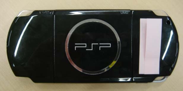
Click to zoom
Application Details
- Equipment Class
- DTS - Digital Transmission System
- Date of Grant
- Jul 13, 2010
- Application Purpose
- Original Equipment
- Date of Application
- Jul 13, 2010
- Equipment Note
- Play Station Portable
- Frequency Range
- 2412.00000000 - 2462.00000000
- Company
- Sony Group Corporation
- Country
- Japan
Documents & Files
Document Text
Text extracted from the exhibit documents filed with the FCC. Open a document above to read the original.
Users Manual
PSP-3001 4-115-362-11(1) PSP-3001 4-115-362-11(1) US/FR/ES Quick Reference Aide-mémoire Referencia rápida PSP-3001 4-115-362-11(1) US/FR/ES This docume ( page 25 Using "XMB" (XrossMediaBar) Introduction GAME Playing games VIDEO Playing video MUSIC Playing music PHOTO Displaying images NETWORK Connecting to the Internet SETTINGS Adjusting PSP ® system settings Direction Us categ P Returns to the Qui t Select to disp button: Category 1 Select a category using the left or right button. 2 Select an item using the up or down button. 3 Press the button to confi rm the selected item. Item Icons displayed in the home menu vary depending on the system software version. The PSP ® system includes a user interface called "XMB" (XrossMediaBar). The main screen for "XMB" is called the “home menu”. Home menu 2 ) US/FR/ES DE IT NL PT PSP-3001 4-115-362-11(1) US/FR/ES US FR ES SELECTSTART VOL This document describes basic operations of the PSP ® system. For detailed instructions, refer to the online user's guide ( page 25): http://manuals.playstation.net/document/ Directional buttons: Used to select categories/items button: Cancels selected operations button: Confi rms selected items PS button: Returns to the home menu Quits gameplay Select an icon, and then press the button to display the options menu. While playing content, press the button to display the control panel. button: Displays the options menu/control panel IconsOptions menuControl panel Category eft or right or down m the me menu”. menu 3 PSP-3001 4-115-362-11(1) US/FR/ES 01 Checking the package contents Preparation Check that you have all of the following items. If any items are missing, visit http://www.us.playstation.com/support or contact SCEA Consumer Services at 1-800-345-7669 for assistance. Additional items may be included with certain models of this product. Please check against the contents listed on the product package. PSP ® (PlayStation ® Portable) system Battery pack AC adaptor AC power cord Printed materials P OW E R H O L D S E L E C T V O L S T A R T About the The PSP ® sy following: • Safety and Before usin It contains s system, trou information • Quick Refe This docum operations • User's Gui (http://manu This online contains de system soft 4 ) US/FR/ES DE IT NL PT PSP-3001 4-115-362-11(1) US/FR/ES FR US ES Preparation Checking the package contents vices at . Please aptor wer cord About the PSP ® system documentation The PSP ® system documentation includes the following: • Safety and Support Before using the product, carefully read this document fi rst. It contains safety information related to the use of the PSP ® system, troubleshooting, specifi cations and other information. • Quick Reference (this document) This document contains information on basic hardware operations of the PSP ® system. • User's Guide (http://manuals.playstation.net/document/) This online document is accessed through the Internet and contains detailed information related to the use of the PSP ® system software ( page 25). 5 PSP-3001 4-115-362-11(1) US/FR/ES 02 Preparing the PSP ® system for use Preparation Charging the battery Before using the PSP ® system for the fi rst time after purchase, you must follow these steps to charge the battery. Caution • The socket-outlet shall be installed near the equipment and shall be easily accessible. • Do not plug the AC power cord for the PSP ® system into an electrical outlet until you have made all other connections. Notice Before inserting the battery pack, fi nd the serial and model numbers listed within the battery compartment and make a record of the numbers for future reference. 1 Remove the battery cover. While holding down the release button, slide the battery cover in the direction of the arrow. 2 1 Release button 2 Insert the battery pack. Align the bottom surface of the battery pack with the system to attach the battery. 1 2 Align the tabs of the battery cover with the system and snap it in place. 4 3 3 Attach battery The powe orange, i has beg u will turn o fully char 6 ) US/FR/ES DE IT NL PT PSP-3001 4-115-362-11(1) US/FR/ES FR US ES Preparation Preparing the PSP ® system for use with the ystem and 3 Attach the AC adaptor to charge the battery. The power indicator lights up in orange, indicating that charging has begun. The power indicator will turn off when the battery is fully charged. Power indicator To electrical outlet SELECTSTART VOL 2 1 3 Initial setup 1 Slide the power/hold switch up. Power/hold switch POW E R HOL D ST A RT S E LE CT The power indicator lights up in green, and the initial setup screen is displayed. 2 Follow the on-screen instructions to make the initial settings. When you have completed initial setup, the home menu ( page 2) is displayed. • See "Using the on-screen keyboard" ( page 26) for information on entering characters. • Settings made during initial setup can be changed later in (Settings). See the user's guide ( page 25) for details. 7 PSP-3001 4-115-362-11(1) US/FR/ES SELECTSTART VOL Using the Press and rele Press for more than one seco *1 : The tone c Also, the t gameplay *2 : To clear m Using the Press and rele Press for more than one seco Press for mor e than fi ve seco *1 : The high e PSP ® syst *2 : To turn th e system bu 03 Part names and functions Preparation System WLAN switch (top) Power/hold switch (right side) ( page 10) Hold indicator ( page 10) Power indicator ( page 10) LCD screen L button Directional buttons Memory Stick Duo™ access indicator ( page 13) WLAN access indicator Lights up when using the wireless LAN feature Analog stick Strap holder PS button Volume – button Volume + button Start button Select button R button button, button button, button Sound button ( page 9) Display button ( page 9) Left speaker Right speaker Microphone ( page 12) USB connector (top) WL A N Off On 8 ) US/FR/ES DE IT NL PT PSP-3001 4-115-362-11(1) US/FR/ES FR US ES Using the sound button Press and release Each time you press the button, the tone changes among HEAVY POP…
Text truncated - open the document above for the full version.
Users Manual
model name1[PSP-3001] [4-115-361-11(1)] masterpage:Right filename[E:\sagyou\4115361111\4115361111\01US\01EN01COV.fm] Safety and Support Sécurité et support technique Seguridad y soporte técnico PSP-3001 4-115-361-11(1) US FR ES 01PSP-1001 EN.book Page 1 Friday, June 20, 2008 11:29 AM masterpage:Left filename[E:\sagyou\4115361111\4115361111\01US\01EN02WAR.fm] 2 WARNINGS model name1[PSP-3001] [4-115-361-11(1)] To avoid electrical shock, do not open the cabinet. Refer servicing to qualified personnel only. For your safety, use only a licensed or genuine Sony AC adaptor or battery charger to charge a battery pack for the PSP ® system. Other types may cause fire, electrical shocks or a malfunc- tion. Caution Use of controls or adjustments or performance of procedures other than those specified herein may result in hazardous radiation exposure. The use of optical instruments with this product will increase eye hazard. This appliance is classified as a CLASS 1 LASER product under IEC60825-1+A2: 2001. This equipment complies with FCC/IC radiation exposure limits set forth for uncontrolled equipment and meets the FCC radio frequency (RF) Exposure Guidelines in Supplement C to OET65 and RSS-102 of the IC radio frequency (RF) Exposure rules. This equipment has very low levels of RF energy that are deemed to comply without testing of specific absorption ratio (SAR). This transmitter must not be co-located or operated in conjunction with any other antenna or transmitter. This Class B digital apparatus complies with Canadian ICES-003. NOTE: This equipment has been tested and found to comply with the limits for a Class B digital device, pursuant to Part 15 of the FCC rules. These limits are designed to provide reasonable protection against harmful interference in a residential installation. This equipment generates, uses, and can radiate radio frequency energy and, if not installed and used in accordance with the instructions, may cause harmful interference to radio communications. However, there is no guarantee that interference will not occur in a particular installation. If this equipment does cause harmful interference to radio or television reception, which can be determined by turning the equipment off and on, the user is encouraged to try to correct the interference by one or more of the following measures: WARNINGS For customers in the U.S.A. and Canada 01PSP-1001 EN.book Page 2 Friday, June 20, 2008 11:29 AM 3 WARNINGS model name1[PSP-3001] [4-115-361-11(1)] masterpage:Right filename[E:\sagyou\4115361111\4115361111\01US\01EN02WAR.fm] US – Reorient or relocate the receiving antenna. – Increase the separation between the equipment and receiver. – Connect the equipment into an outlet on a circuit different from that to which the receiver is connected. – Consult the dealer or an experienced radio/TV technician for help. You are cautioned that any changes or modifications not expressly approved by the party responsible for compliance could void the user's authority to operate the equipment. A very small percentage of individuals may experience epileptic seizures or blackouts when exposed to certain light patterns or flashing lights. Exposure to certain patterns or backgrounds on a screen or when playing video games may trigger epileptic seizures or blackouts in these individuals. These conditions may trigger previously undetected epileptic symptoms or seizures in persons who have no history of prior seizures or epilepsy. If you, or anyone in your family, has an epileptic condition or has had seizures of any kind, consult your physician before playing. IMMEDIATELY DISCONTINUE use and consult your physician before resuming gameplay if you or your child experience any of the following health problems or symptoms: • dizziness, • altered vision, • eye or muscle twitches, • loss of awareness, • disorientation, • seizures, or • any involuntary movement or convulsion. RESUME GAMEPLAY ONLY ON APPROVAL OF YOUR PHYSICIAN. Use and handling of video games to reduce the likelihood of a seizure • Use in a well-lit area and keep the screen a safe distance from your face. • Avoid prolonged use of the PSP® system. Take a 15-minute break during each hour of play. • Avoid playing when you are tired or need sleep. If you have questions about this product, call our technical support line at 1-800-345-7669, or write to: Sony Computer Entertainment America Inc. Consumer Services/Technical Support PO Box 5888, San Mateo, CA 94402-0888 U.S.A. This device complies with Part 15 of the FCC Rules and RSS- Gen of IC Rules. Operation is subject to the following two conditions: (1) this device may not cause harmful interference, and (2) this device must accept any interference received, including interference that may cause undesired operation of this device. Declaration of Conformity Trade Name : Model No. : Responsible Party : Address : Telephone No. : SONY PSP-3001 Sony Electronics Inc. 16530 Via Esprillo, San Diego, CA 92127 U.S.A 858-942-2230 Photosensitivity/Epilepsy/Seizures 01PSP-1001 EN.book Page 3 Friday, June 20, 2008 11:29 AM masterpage:Left filename[E:\sagyou\4115361111\4115361111\01US\01EN02WAR.fm] 4 WARNINGS model name1[PSP-3001] [4-115-361-11(1)] Radio waves may affect electronic equipment or medical devices (for example, pacemakers), which may cause malfunctions and possible injuries. • If you use a pacemaker or other medical device, consult your physician or the manufacturer of your medical device before using the wireless LAN feature. • Do not use the wireless LAN feature in the following locations: – Areas where wireless LAN use is prohibited, such as in hospitals. Abide by medical institution regulations when using the system on their premises. – Areas near fire alarms, automatic doors and other types of automated equipment. Sony Computer Entertainment Inc. uses DNAS (Dynamic Network Authentication System), a proprietary authentication system, to help protect copyright and security in connecting the PSP ® syst…
Text truncated - open the document above for the full version.
External Photos
Outside(1) SC EI Co nfi d ential Outside(2) SC EI Co nfi d ential
ID Label/Location Info
FCC ID will be affixed on the outside of device. The regulatory compliance label is visible to the end user at the time of purchase. FCC ID: AK8PSP3001D
Internal Photos
Inside(1) ANTENNA(Back Side) WLAN Module(Back Side) SC EI Co nfi d ential Inside (2) PWB Rear-side ANTENNAWLAN Module SC EI Co nfi d ential WLAN Module With Shield Without Shield Rear Side
Test Report
Test report No. : 30JE0236-HO-01-A Page : 1 of 38 Issued date : July 8, 2010 FCC ID : AK8PSP3001D UL Japan, Inc. Head Office EMC Lab. 4383-326 Asama-cho, Ise-shi, Mie-ken 516-0021 JAPAN Telephone : +81 596 24 8116 Facsimile : +81 596 24 8124 RADIO TEST REPORT Test Report No. : 30JE0236-HO-01-A Applicant : Sony Computer Entertainment Inc. Type of Equipment : PSP Model No. : PSP-3001 FCC ID : AK8PSP3001D Test regulation : FCC Part 15 Subpart C 2010 Test Result : Complied 1. This test report shall not be reproduced in full or partial, without the written approval of UL Japan, Inc. 2. The results in this report apply only to the sample tested. 3. This sample tested is in compliance with the above regulation. 4. The test results in this report are traceable to the national or international standards. 5. This test report must not be used by the customer to claim product certification, approval, or endorsement by NVLAP, NIST, or any agency of the Federal Government. Date of test: _____________________________ Representative test engineer: _____________________________ Takumi Shimada Engineer of EMC Service Approved by: _____________________________ Mitsuru Fujimura Manager of EMC Service MF060b (10.05.10) NVLAP LAB CODE: 200572-0 This laboratory is accredited by the NVLAP LAB CODE 200572-0, U.S.A. The tests reported herein have been performed in accordance with its terms of accreditation. *As for the range of Accreditation in NVLAP, you may refer to the WEB address, http://www.ul.com/japan/jpn/pages/services/emc/about/ma rk1/index.jsp#nvlap June 9 to 24, 2010 Test report No. : 30JE0236-HO-01-A Page : 2 of 38 Issued date : July 8, 2010 FCC ID : AK8PSP3001D UL Japan, Inc. Head Office EMC Lab. 4383-326 Asama-cho, Ise-shi, Mie-ken 516-0021 JAPAN Telephone : +81 596 24 8116 Facsimile : +81 596 24 8124 CONTENTS PAGE SECTION 1: Customer information.........................................................................................................3 SECTION 2: Equipment under test (E.U.T.)...........................................................................................3 SECTION 3: Test specification, procedures & results............................................................................4 SECTION 4: Operation of E.U.T. during testing ....................................................................................8 SECTION 5: Conducted Emission..........................................................................................................11 SECTION 6: Radiated Spurious Emission ............................................................................................12 SECTION 7: Antenna Terminal Conducted Tests................................................................................13 APPENDIX 1: Photographs of test setup ...............................................................................................14 Conducted Emission .........................................................................................................................14 Radiated Spurious Emission .............................................................................................................15 Worst Case Position (Horizontal: X-axis/ Vertical:Z-axis) ..............................................................16 APPENDIX 2: Data of EMI test..............................................................................................................19 Conducted Emission .........................................................................................................................19 6dB Bandwidth .................................................................................................................................22 Maximum Peak Output Power ..........................................................................................................24 Radiated Spurious Emission .............................................................................................................25 Conducted Spurious Emission ..........................................................................................................30 Conducted Emission Band Edge compliance ...................................................................................34 Power Density ...................................................................................................................................35 99%Occupied Bandwidth .................................................................................................................37 APPENDIX 3: Test instruments .............................................................................................................38 Test report No. : 30JE0236-HO-01-A Page : 3 of 38 Issued date : July 8, 2010 FCC ID : AK8PSP3001D UL Japan, Inc. Head Office EMC Lab. 4383-326 Asama-cho, Ise-shi, Mie-ken 516-0021 JAPAN Telephone : +81 596 24 8116 Facsimile : +81 596 24 8124 SECTION 1: Customer information Company Name Sony Computer Entertainment Inc. Brand name Sony Address 2-6-21 Minami-Aoyama, Minato-ku, Tokyo, 107-0062, Japan Telephone Number +81-3-6483-8023 Facsimile Number +81-3-6483-8642 Contact Person Tatsuya Suzuki SECTION 2: Equipment under test (E.U.T.) 2.1 Identification of E.U.T. Type of Equipment PSP Model No. PSP-3001 Serial No. 03-TSP1700H-0000301-PSPXXXX for Conducted Emission and Radiated Emission tests 03-TSP1700H-0000314-PSPXXXX for Antenna Terminal Conducted tests Rating DC 5V, AC Adaptor (AC 100V-240V) Country of Manufacture China Receipt Date of Sample May 31, 2010 Condition of EUT Production prototype (Not for sale: This sample is equivalent to mass-produced items.) Modification of EUT No modification by the test lab. 2.2 Product Description Radio Specification Wireless LAN Module (IEEE802.11b) Equipment Type Transceiver Frequency of Operation 2412-2462 MHz Clock Frequency 40MHz ITU Code G1D Type of Modulation DSSS Method of frequency generation Crystal Antenna model EBMGC5A245FB Antenna ty…
Text truncated - open the document above for the full version.
Test Report
Test report No. : 30JE0236-HO-01-A Page : 19 of 38 Issued date : July 8, 2010 FCC ID : AK8PSP3001D UL Japan, Inc. Head Office EMC Lab. 4383-326 Asama-cho, Ise-shi, Mie-ken 516-0021 JAPAN Telephone : +81 596 24 8116 Facsimile : +81 596 24 8124 APPENDIX 2: Data of EMI test Conducted Emission DATA OF CONDUCTED EMISSION TEST UL Japan, Inc. Head Office EMC Lab. No.4 Semi Anechoic Chamber Date : 2010/06/10 Company : Sony Computer Entertainment Inc. Report No. : 30JE0236-HO-01 Kind of EUT : PSP Power : AC 120V / 60Hz Model No. : PSP-3001 Temp./Humi. : 23deg.C / 54% Serial No. : 03-TSP1700H-0000301-PSPXXXX Engineer : Takeshi Choda Mode / Remarks : WLAN 11b, Tx 2412MHz, 11Mbps LIMIT : FCC15.207 QP FCC15.207 AV CHART:WITH FACTOR,Peak hold data. CALCULATION:RESULT[dBuV]=READING[dBuV]+C.F[dB](LISN LOSS+CABLE LOSS) Except for the above table : adequate margin data below the limits. Frequency[Hz] [dBuV]<< QP/AV DATA >> L:QP:AV N:QP:AV .15M30M.2M.3M.5M.7M1M2M3M5M7M10M20M 0 10 20 30 40 50 60 70 80 Frequency Reading LevelReading LevelCorr.ResultsResultsLimitLimitMarginMargin PhaseComment Frequency QPAVFactorQPAVQPAVQPAVPhaseComment [MHz][dBuV][dBuV][dB][dBuV][dBuV][dBuV][dBuV][dB][dB] PhaseComment 0.1997331.120.513.344.433.863.653.619.219.8N 0.2982021.58.213.334.821.560.350.325.528.8N 0.4951217.70.613.331.013.956.146.125.132.2N 0.7013218.60.813.331.914.156.046.024.131.9N 3.2100815.10.213.528.613.756.046.027.432.3N 20.5588614.710.414.829.525.260.050.030.524.8N 0.1997332.122.013.345.435.363.653.618.218.3L 0.2974024.49.713.337.723.060.350.322.627.3L 0.4914019.31.313.332.614.656.146.123.531.5L 0.7124020.61.813.333.915.156.046.022.130.9L 3.1916714.3-0.213.527.813.356.046.028.232.7L 20.6790014.310.514.829.125.360.050.030.924.7L Test report No. : 30JE0236-HO-01-A Page : 20 of 38 Issued date : July 8, 2010 FCC ID : AK8PSP3001D UL Japan, Inc. Head Office EMC Lab. 4383-326 Asama-cho, Ise-shi, Mie-ken 516-0021 JAPAN Telephone : +81 596 24 8116 Facsimile : +81 596 24 8124 Conducted Emission Test place Head Office EMC Lab. No.4 Semi Anechoic Chamber Report No. 30JE0236-HO-01 Date 06/09/2010 Temperature/ Humidity 23 deg.C./ 54% Engineer Takeshi Choda Mode 11b Tx 2412MHz 2437MHz 2462MHz Y scale [dBuV] Chart N L Test report No. : 30JE0236-HO-01-A Page : 21 of 38 Issued date : July 8, 2010 FCC ID : AK8PSP3001D UL Japan, Inc. Head Office EMC Lab. 4383-326 Asama-cho, Ise-shi, Mie-ken 516-0021 JAPAN Telephone : +81 596 24 8116 Facsimile : +81 596 24 8124 Conducted Emission DATA OF CONDUCTED EMISSION TEST UL Japan, Inc. Head Office EMC Lab. No.4 Semi Anechoic Chamber Date : 2010/06/10 Company : Sony Computer Entertainment Inc. Report No. : 30JE0236-HO-01 Kind of EUT : PSP Power : AC 120V / 60Hz Model No. : PSP-3001 Temp./Humi. : 23deg.C / 54% Serial No. : 03-TSP1700H-0000301-PSPXXXX Engineer : Takeshi Choda Mode / Remarks : WLAN 11b, Rx 2437MHz, 11Mbps LIMIT : FCC15.207 QP FCC15.207 AV CHART:WITH FACTOR,Peak hold data. CALCULATION:RESULT[dBuV]=READING[dBuV]+C.F[dB](LISN LOSS+CABLE LOSS) Except for the above table : adequate margin data below the limits. Frequency[Hz] [dBuV]<< QP/AV DATA >> L:QP:AV N:QP:AV .15M30M.2M.3M.5M.7M1M2M3M5M7M10M20M 0 10 20 30 40 50 60 70 80 Frequency Reading LevelReading LevelCorr.ResultsResultsLimitLimitMarginMargin PhaseComment Frequency QPAVFactorQPAVQPAVQPAVPhaseComment [MHz][dBuV][dBuV][dB][dBuV][dBuV][dBuV][dBuV][dB][dB] PhaseComment 0.1985530.319.313.343.632.663.753.720.121.1N 0.2993520.87.913.334.121.260.350.326.229.1N 0.5078017.70.313.331.013.656.046.025.032.4N 0.7268017.0-1.313.330.312.056.046.025.734.0N 3.3275711.5-1.413.525.012.156.046.031.033.9N 20.7230014.010.414.828.825.260.050.031.224.8N 0.1985531.320.613.344.633.963.753.719.119.8L 0.2993523.88.413.337.121.760.350.323.228.6L 0.5078019.82.113.333.115.456.046.022.930.6L 0.7268020.81.413.334.114.756.046.021.931.3L 3.3275712.3-0.713.525.812.856.046.030.233.2L 20.7230014.310.414.829.125.260.050.030.924.8L Test report No. : 30JE0236-HO-01-A Page : 22 of 38 Issued date : July 8, 2010 FCC ID : AK8PSP3001D UL Japan, Inc. Head Office EMC Lab. 4383-326 Asama-cho, Ise-shi, Mie-ken 516-0021 JAPAN Telephone : +81 596 24 8116 Facsimile : +81 596 24 8124 6dB Bandwidth Test place Head Office EMC Lab. No.7 Shielded Room Report No. 30JE0236-HO-01 Date 06/18/2010 Temperature/ Humidity 24 deg.C./ 58% Engineer Takumi Shimada Mode 11b, Tx(Ch L,M,H), 11Mbps 11b Frequency 6dB Bandwidth Limit [MHz] [MHz] [kHz] 2412 9.934 >500 2437 9.956 >500 2462 9.525 >500 Test report No. : 30JE0236-HO-01-A Page : 23 of 38 Issued date : July 8, 2010 FCC ID : AK8PSP3001D UL Japan, Inc. Head Office EMC Lab. 4383-326 Asama-cho, Ise-shi, Mie-ken 516-0021 JAPAN Telephone : +81 596 24 8116 Facsimile : +81 596 24 8124 6dB Bandwidth 11b 2412MHz 2437MHz 2462MHz Test report No. : 30JE0236-HO-01-A Page : 24 of 38 Issued date : July 8, 2010 FCC ID : AK8PSP3001D UL Japan, Inc. Head Office EMC Lab. 4383-326 Asama-cho, Ise-shi, Mie-ken 516-0021 JAPAN Telephone : +81 596 24 8116 Facsimile : +81 596 24 8124 Maximum Peak Output Power Test place Head Office EMC Lab. No.7 Shielded Room Report No. 30JE0236-HO-01 Date 06/24/2010 Temperature/ Humidity 23 deg.C./ 59% Engineer Takumi Shimada Mode 11b Tx Freq.ReadingCableAtten.Margin Loss [MHz][dBm][dB][dB][dBm][mW][dBm][mW][dB] 24120.680.5010.0011.1813.1230.00100018.82 24371.220.5010.0011.7214.8630.00100018.28 24620.560.5010.0011.0612.7630.00100018.94 Sample Calculation: Result = Reading + Cable Loss (customer supplied) + Attenuator Antenna 1, 2437MHz RateReading Remark [Mbps][dBm] 11.17 21.09 5.50.61 111.22* *: Worst Rate All comparizon were carried out on same frequency and measurement factors. ResultLimi t Test report No. : 30JE0236-HO-01-A Page : 25 of 38 Issued date : July 8, 2010 FCC ID : AK8PSP3001D UL Japan, Inc. Head Office EMC Lab. 4383-326 Asama-cho, Ise-shi, Mie-ken 516-0021 JAPAN Telephone : +81 596 24 8116 Facsimile : +81 596 24 8124 Radiated Spurious Emission Test place Head Office EMC Lab. No.4 Semi Anechoic Chamber Report No. 30JE02…
Text truncated - open the document above for the full version.
Test Setup Photos
Test report No. : 30JE0236-HO-01-A Page : 14 of 38 Issued date : July 8, 2010 FCC ID : AK8PSP3001D UL Japan, Inc. Head Office EMC Lab. 4383-326 Asama-cho, Ise-shi, Mie-ken 516-0021 JAPAN Telephone : +81 596 24 8116 Facsimile : +81 596 24 8124 APPENDIX 1: Photographs of test setup Conducted Emission Photo 1 Photo 2 Test report No. : 30JE0236-HO-01-A Page : 15 of 38 Issued date : July 8, 2010 FCC ID : AK8PSP3001D UL Japan, Inc. Head Office EMC Lab. 4383-326 Asama-cho, Ise-shi, Mie-ken 516-0021 JAPAN Telephone : +81 596 24 8116 Facsimile : +81 596 24 8124 Radiated Spurious Emission Photo 1 Photo 2 Test report No. : 30JE0236-HO-01-A Page : 16 of 38 Issued date : July 8, 2010 FCC ID : AK8PSP3001D UL Japan, Inc. Head Office EMC Lab. 4383-326 Asama-cho, Ise-shi, Mie-ken 516-0021 JAPAN Telephone : +81 596 24 8116 Facsimile : +81 596 24 8124 Worst Case Position (Horizontal: X-axis/ Vertical:Z-axis) X-axis Y-axis Z-axis Test report No. : 30JE0236-HO-01-A Page : 17 of 38 Issued date : July 8, 2010 FCC ID : AK8PSP3001D UL Japan, Inc. Head Office EMC Lab. 4383-326 Asama-cho, Ise-shi, Mie-ken 516-0021 JAPAN Telephone : +81 596 24 8116 Facsimile : +81 596 24 8124 Configuration and peripherals : Standard Ferrite Core AC120V/60Hz AC120V/60Hz AC120V/60Hz 1 A DF H E G J I 6 8 7 9 2 3 4 5 B C * Cabling and setup were taken into consideration and test data was taken under worse case conditions. Test report No. : 30JE0236-HO-01-A Page : 18 of 38 Issued date : July 8, 2010 FCC ID : AK8PSP3001D UL Japan, Inc. Head Office EMC Lab. 4383-326 Asama-cho, Ise-shi, Mie-ken 516-0021 JAPAN Telephone : +81 596 24 8116 Facsimile : +81 596 24 8124 Description of EUT and Support equipment No. Item Model number Serial number Manufacturer Remarks A PSP PSP-3001 03-TSP1700H-0000301-PSPXXXX *1) 03-TSP1700H-0000314-PSPXXXX *2) Sony Computer Entertainment Inc. EUT B Memory Stick Duo MSX-M512S - SONY - C Battery Pack PSP-S110 (PSP-S110 B) 10209WBB1545 SONY - D Laptop PC 2371-4WJ KV-04455 IBM - E AC Adaptor 02K6808 11S02K6808Z1Z89H3C6HWN IBM - F Hub FX-05Mini - PLANEX - G Adaptor for Hub RHF-050080-1 0643 PLANEX - H HP Remote Controller PSP-S120 - MITSUMI - I Headphones PSP-130 - SONY - J AC Adaptor PSP-380 (ACC-195) 10040000187A SONY EUT *1) Used for Conducted Emission and Radiated Emission tests *2) Used for Antenna Terminal Conducted tests List of cables used No. Name Length (m) Shield Cable Connector 1 USB Cable 0.5 Shielded Shielded 2 HP Remote Controller 0.8 Shielded Shielded 3 Headphones Cable 1.1 Shielded Shielded 4 DC Cable 1.0 Shielded Shielded 5 AC Cable 1.5 Unshielded Unshielded 6 LAN Cable 3.0 Unshielded Unshielded 7 DC Cable 1.7 Unshielded Unshielded 8 DC Cable 1.8 Shielded Shielded 9 AC Cable 1.0 Unshielded Unshielded
Contact Information
Applicant
Kazuyuki Hori(Chief EMC/RF Compliance Specialist)
Test Firm
UL Japan, Inc. Head office EMC Lab.Tetsuya Hashimoto
Technical Specifications
| # | Rule Parts | Frequency Range | Power Output |
|---|---|---|---|
| 1 | 15C | 2.41 GHz - 2.46 GHz | 15.00 mW |
Other Applications from Sony Group Corporation
AK8WW81782
Aug 21, 2026Radio Equipment
Equipment Class
DSS - Part 15 Spread Spectrum TransmitterAK8CFIZCP2
Aug 03, 2026Wireless Controller
Equipment Class
DSS - Part 15 Spread Spectrum TransmitterAK8OEV321MUH
Apr 14, 2026LCD Monitor
Equipment Class
JAD - Part 15 Class A Digital DeviceAK8OEV431MUH
Apr 14, 2026LCD Monitor
Equipment Class
JAD - Part 15 Class A Digital DeviceAK8OEV271MUH
Apr 14, 2026LCD Monitor
Equipment Class
JAD - Part 15 Class A Digital Device