AK8S430CSony Remote Card System Reader/Writer RC-S430C
Sony Group Corporation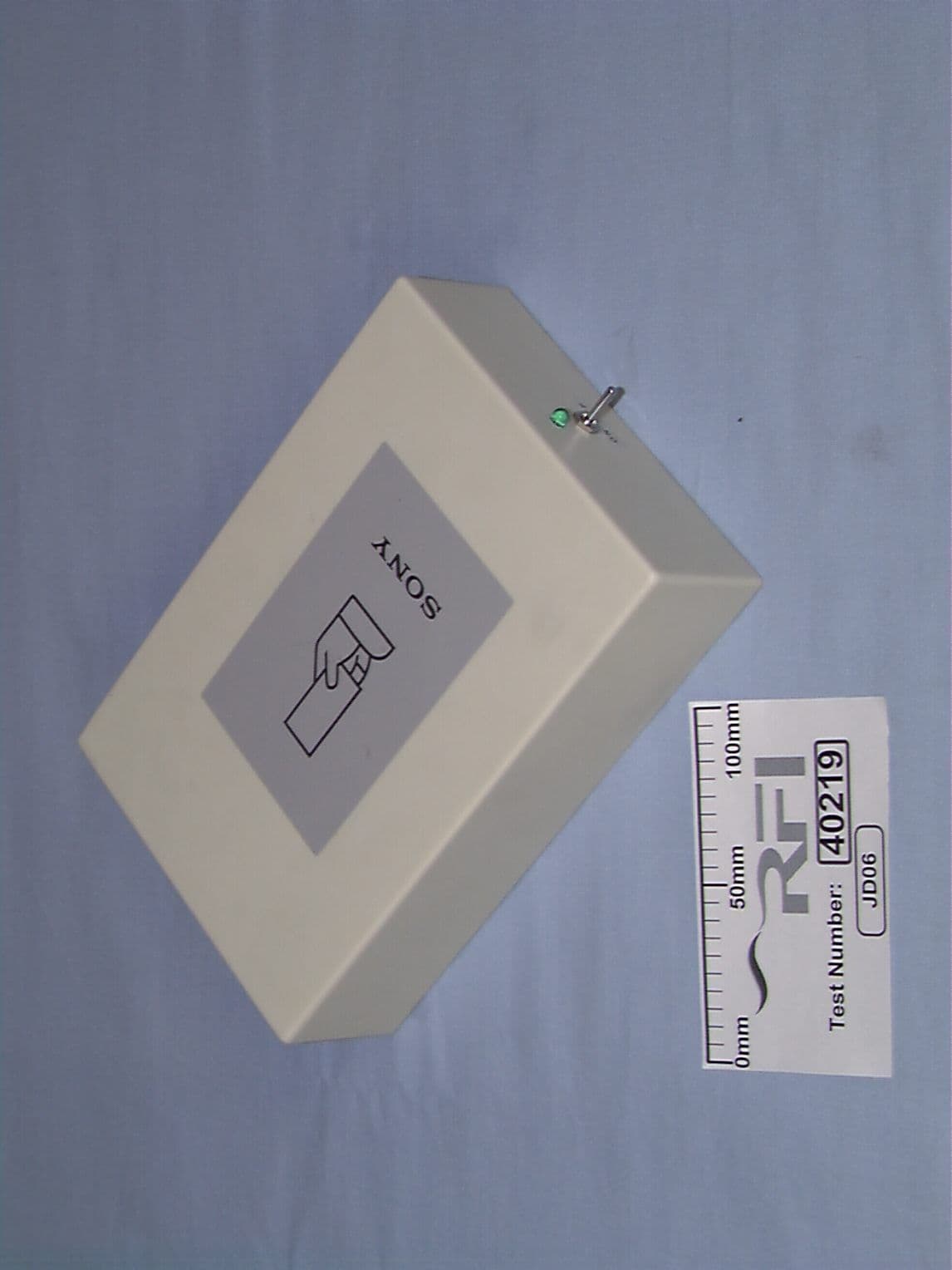
Click to zoom
Application Details
- Equipment Class
- DXX - Part 15 Low Power Communication Device Transmitter
- Date of Grant
- Feb 15, 2000
- Application Purpose
- Original Equipment
- Date of Application
- Jan 23, 2000
- Equipment Note
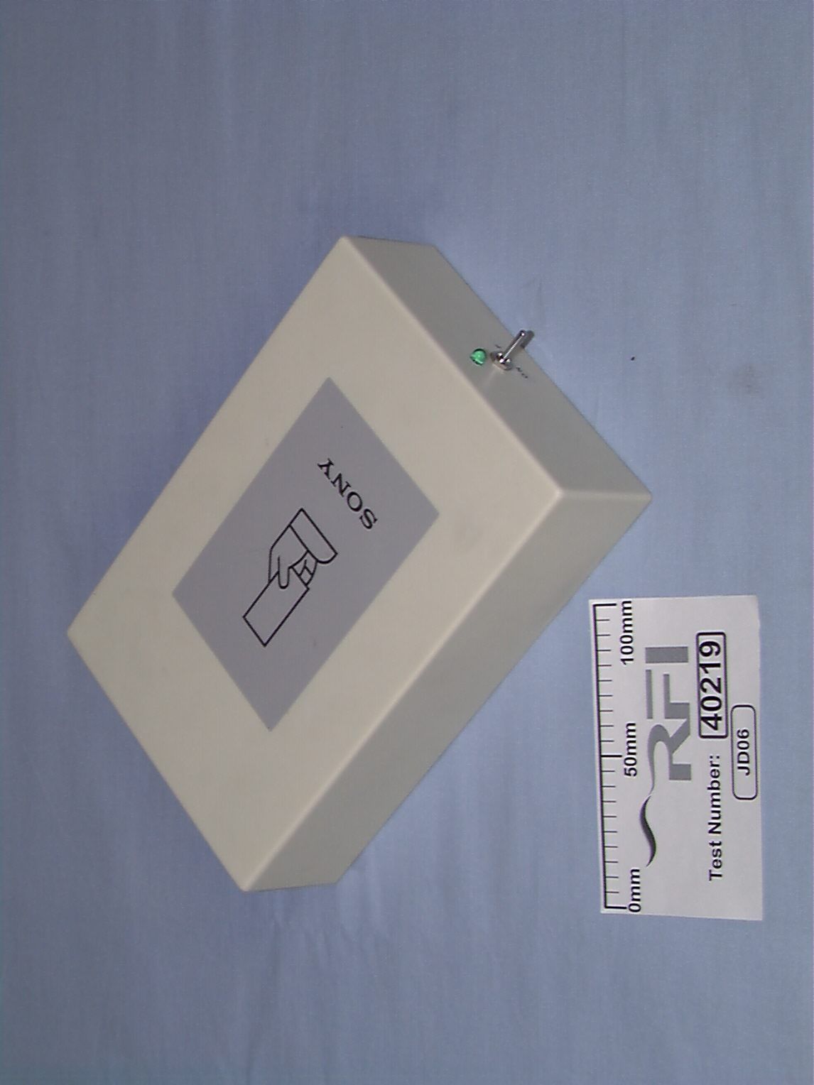
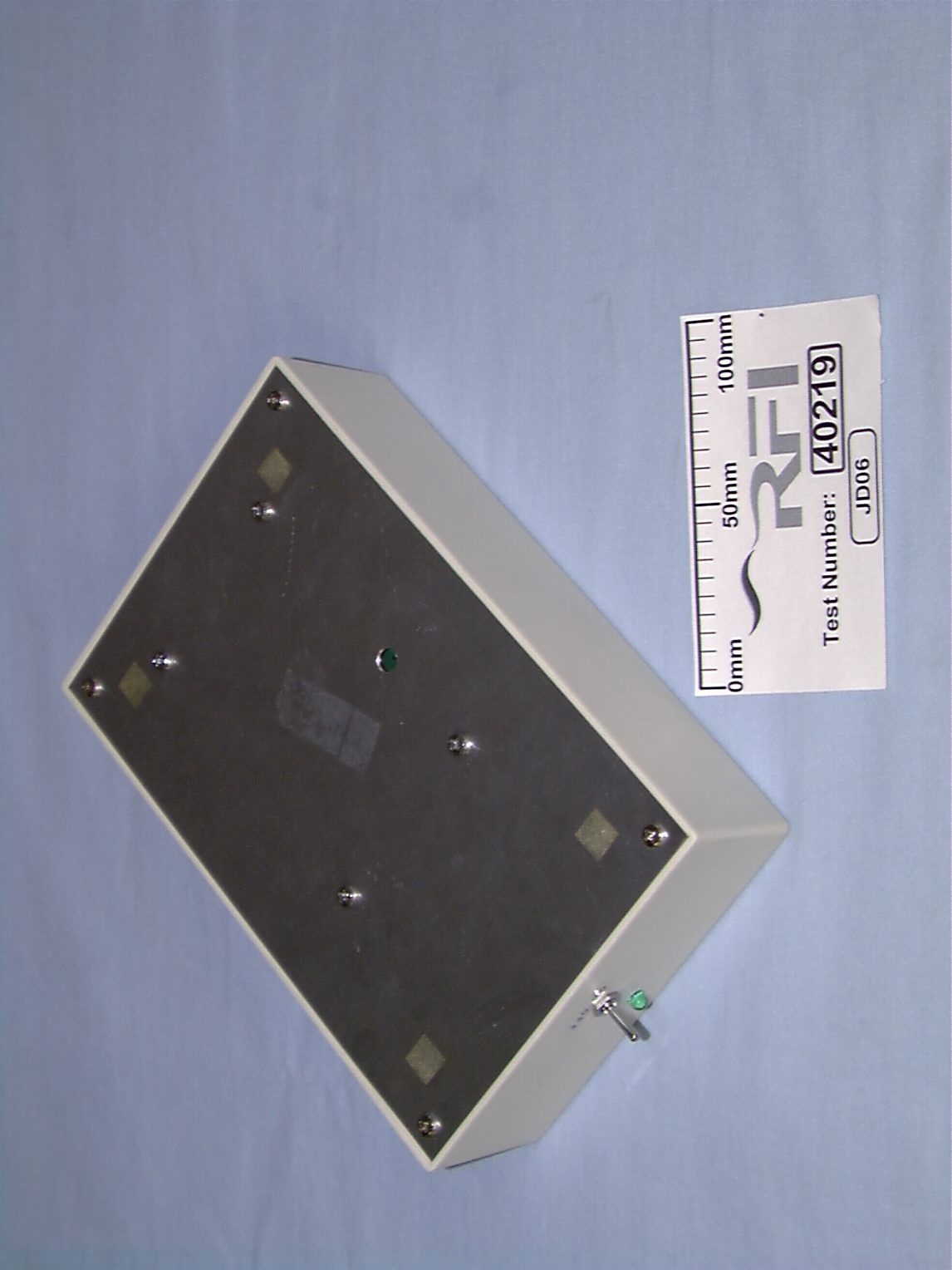
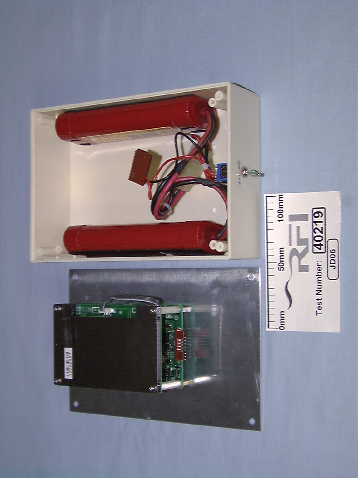
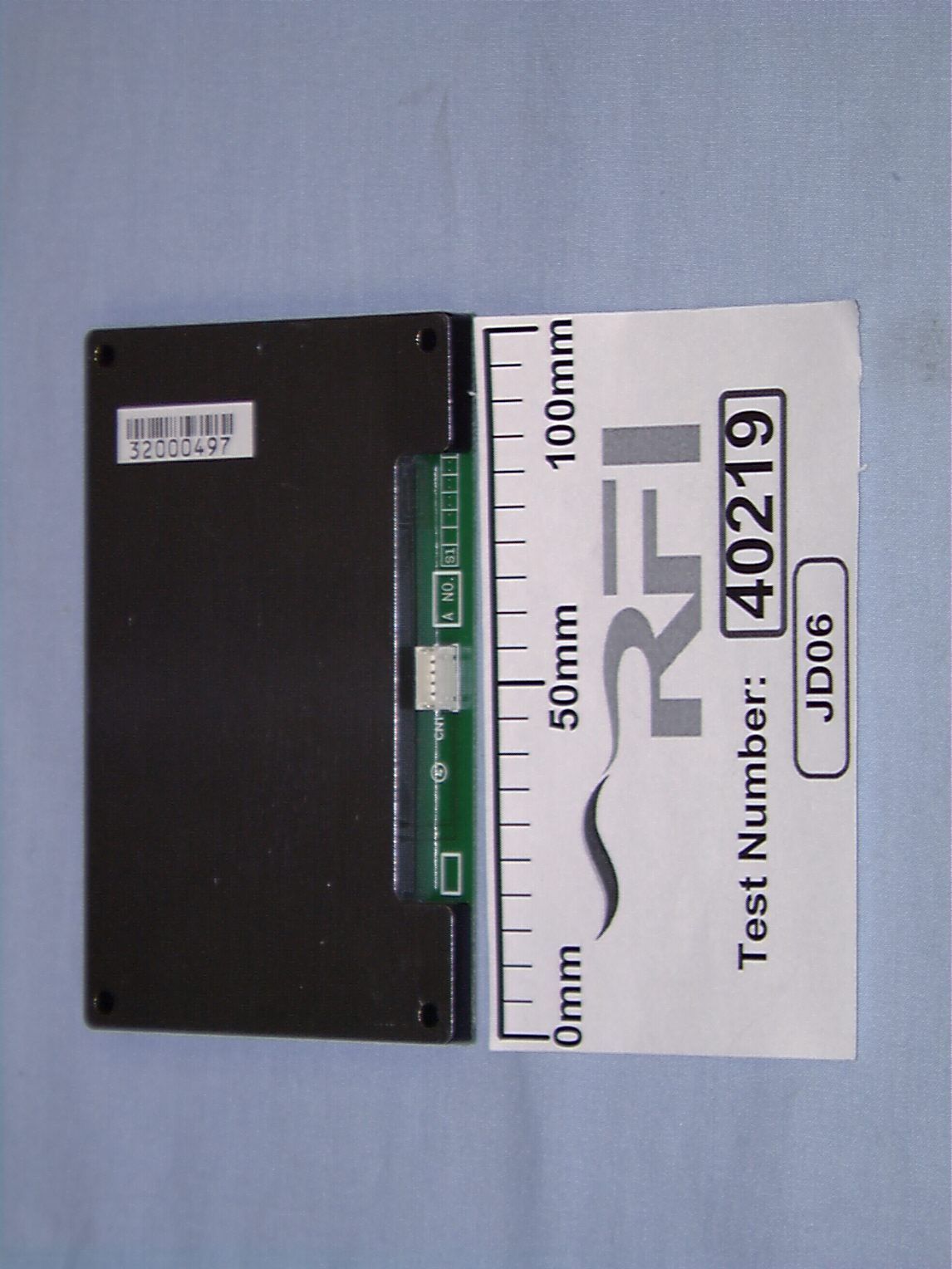
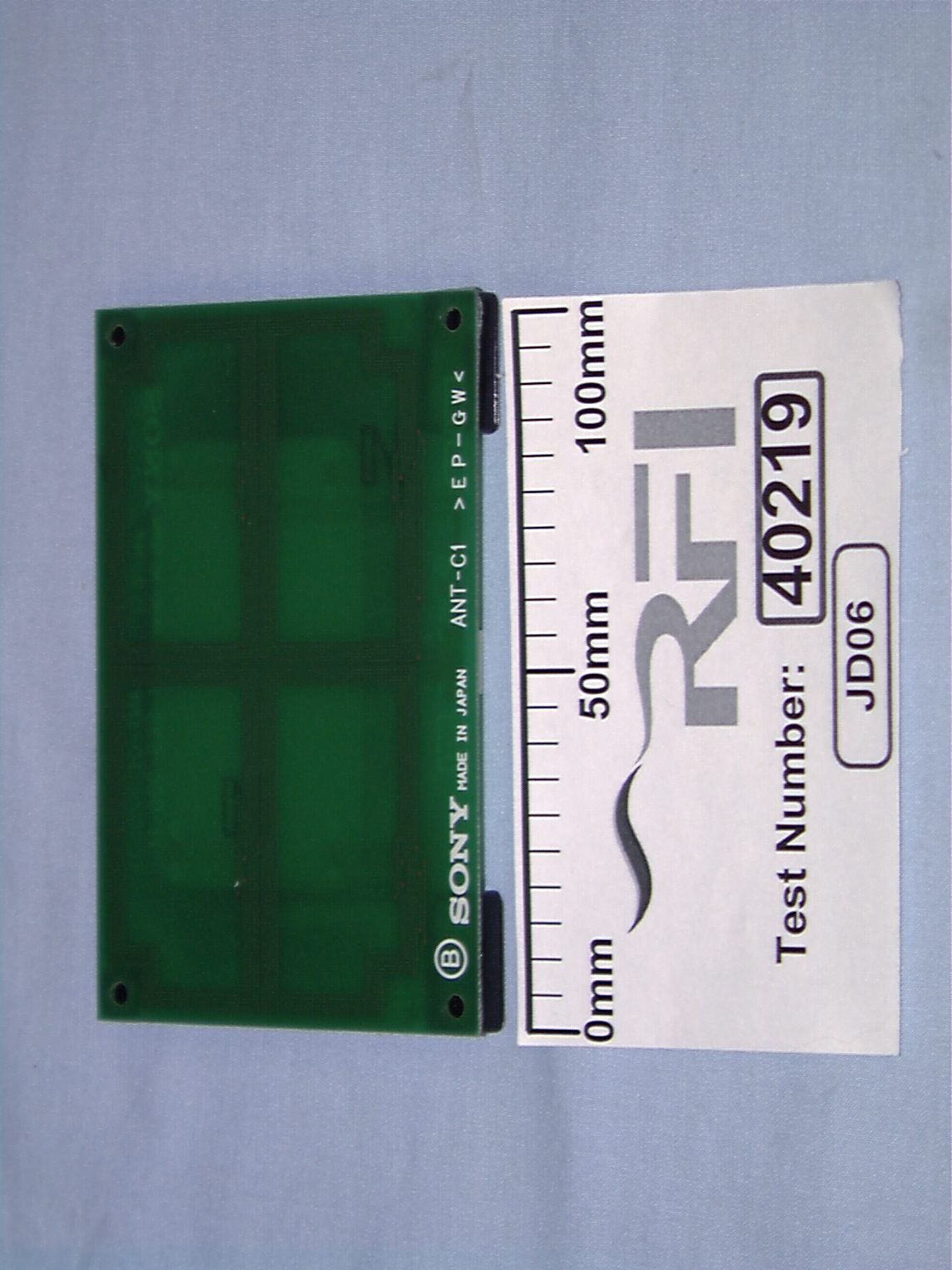
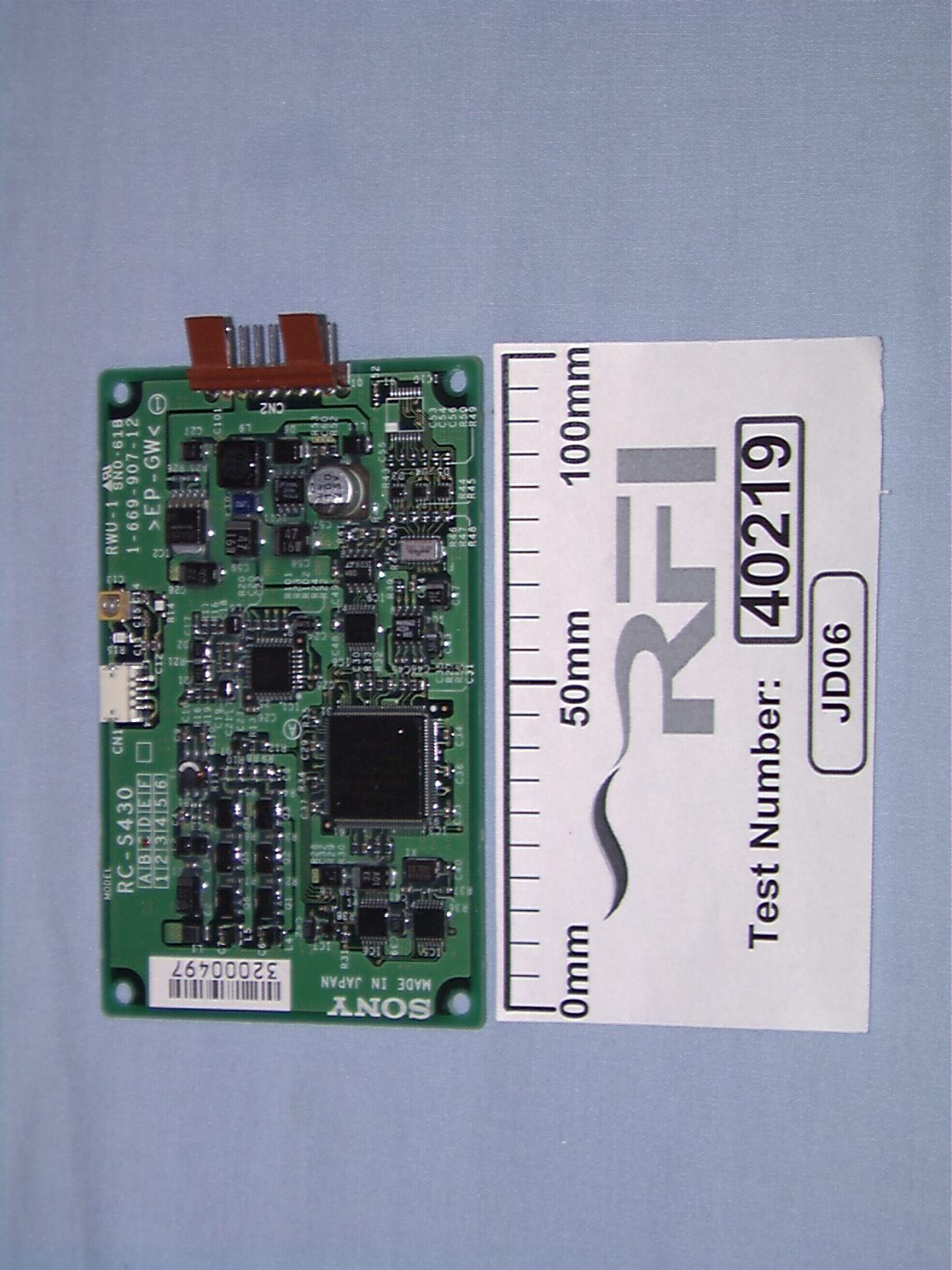
- Sony Remote Card System Reader/Writer RC-S430C
- Frequency Range
- 13.56000000 - 13.56000000
- Company
- Sony Group Corporation
- Country
- Japan
Documents & Files
Document Text
Text extracted from the exhibit documents filed with the FCC. Open a document above to read the original.
Block Diagram
Digital Processing Unit Signal Processing Unit Memory DC-DC Converter Antenna Unit TuningCircuit 11V (only for Power Amp.) 13.56MHz Oscillator Clock 5V 12 or 5V MAX662 CXD8680R CXA3175Q RD *WD *R/W RS-485 Driver EMI filter & Protection Circuit Switching Regulator Series Regulator 5V EXT DC (typ. 12V) LTC490 RS-485 CMOS 5V EXT CPU LM2594M-5.0 PQ20VZ51 Power Amp. & Modulation EN/*INH Block Diagram of RC-S430C Detector Low Pass Filter Band Pass Filter Amplifier Threshold Detector
ID Label/Location Info
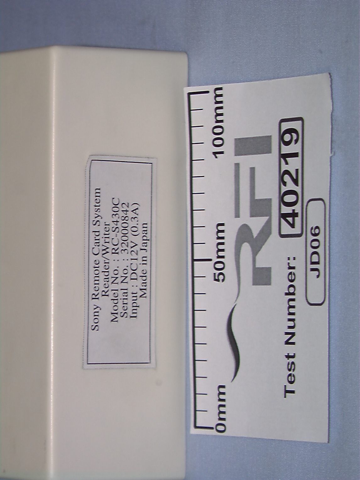
Sony Remote Card System Reader/Writer Model No.:RC-S430C Serial No.:32000482 FCC ID: AK8S430C Made in Japan Label layout for RC-S430C 65mm 25mm 10mm 15mm 32mm32mm
Operational Description
Operational Description - Model RC-S430C - Version 1.0 Sony Corporation RC-S430C Operational Description 2 Reader/Writer Operation After turning on the power switch, the Reader/Writer transmits 13.56MHz 10% ASK polling signal with the specified intensity until receiving a response from a contactless card. After receiving the response from a card the device starts to communicate with the card by using the same frequency and modulation. Though the reader/writer is a self- operating device according to the program installed in the FLASH memory, it can be connected to a host computer (Controller) for more complicated applications by taking out the reader/writer from the enclosure. For the connection to a host computer, refer to the initialization and communication protocols described below. 1Connection with Controller The connection with controller shall be done as follows. •Interface Connector : Methode 1100-12-110-02 (right angle) The interface connector is a 10-pin connector located at the right edge of the RF/Control board which is shown in the schematic drawing of Fig.6. The pitch of connector pins is 2.54mm. The most upper connector pin is No. 1. Pin assignment of the connector is shown in Fig. 4 and Table 4. 12V:DC input port GND:Ground port SHDN :Shut Down (No Connection in usual operation) Power supply for the circuit on the RF/Control board can be shut down by applying high level voltage (5V) to the pin. RX+,- , TX+,-:Serial Data I/O (RS-485) RXD,TXD:Serial Data I/O (CMOS 5V or RS-232C) Fig.1 : Pin Assignment of Connectors CN1-2 Pin No. 12345678910 Pin AssignmentSHDNGNDDCINRX-RX+TX-TX+TXDGNDRXD Table 1 : Pin Assignment of Interface Connector CN2 RF block RFIN+ RFIN- RFOUT- RFOUT+ WD RD *R/W CARRIER EN/*INH DC GND 5V Controller WD RD *R/W CARRIER EN/*INH GND 5V RXD TXD TX+ TX- RX+ RX- Converter GND5V DC SHDN to Antenna RX-(RS485) TX-(RS485) RXD(CMOS or RS232C) DCIN GND TX+(RS485) RX+(RS485) GND TXD(CMOS or RS232C) SHDN CN1 1 2 3 4 CN2 1 2 3 4 5 6 7 8 9 10 RC-S430C Operational Description 3 •Power voltage : DC12V (shall be applied to DCIN of CN2) voltage allowance : +4V, -0.5V current:≈ 180mA voltage ripple allowance:100mV (peak-to-peak) The Reader/Writer can be operated in the voltage range of 7-11.5V and the voltage ripple > 100mV, however operating distance cannot be assured in such condition. •External Interface serial 1 port : RS-485A, RS-232C and CMOS logic level(5V) software selectable, non-inverted or inverted, and baud rate (default setting : CMOS 5V, non-inverted, 115.2kbps) Common pins are assigned for RS-232C and CMOS logic level. RS-232C is available by mounting MAX3221CAE(MAXIM) as IC10, 4 capacitors C53-56 and 2 resistors R49-50 and removing 2 resistors R43-44 which are located near the right, lower corner of the RF/Control board as is shown in Fig.5. 2Transaction Overview 2.1 Communication Protocol There are two communication protocols, namely, data link level and application level protocol. Either ACK or NACK packet is returned in every packet transfer. ACK indicates a successful transfer, NACK means unsuccessful. Fig. 2 : Communication Protocol and Packet Structure 2.2 Re-sending Protocol Reader/Writer supports the re-sending procedure in Controller interface. Re-sending handling is triggered or required in the two cases below : 1. NACK packet is returned. 2. Neither ACK nor NACK response comes. (time out) Controller should re-send the same packet within 5ms after receiving NACK or detecting time out. 2.3ACK / NACK Packet ACK / NACK packet format is as follows : Reader/WriterController Max. 2ms Command Packet ACK ACK Max. 2ms Response Packet 00FF00 LEN LCS PD0PDnPD1DCS 00 ... Postamble Packet Data Checksum Packet Data Packet Length Checksum Start of Packet Code Packet Length Preamble Command or Response Code RC-S430C Operational Description 4 ACK : LEN = 00h & LCS = ffh without Packet Data part and DCS NACK : LEN = ffh & LCS = 00h without Packet Data part and DCS 2.4 Mutual Authentication Mutual Authentication is a process that is performed between Controller and Reader/Writer to authenticate each other mutually in order to avoid the fraud usage. This authentication is based on the following elements : 1. two 8byte (64bit) keys 2. three pass authentication model (ISO 9758) 3. cryptography algorithm mentioned in section 3.2.5. 2.5 Encryption and Decryption The cryptography algorithm is used for the following three stages : 1. mutual authentication between Controller and Reader/Writer 2. mutual authentication between Reader/Writer and Card 3. commands and data encryption through Reader/Writer 3Communication Commands 3.1General In this section, the communication commands between Controller and Reader /Writer are described. Table 1-3 shows all commands between Controller and general Reader/Writer. All commands are categorized into 3 groups as follows : 1. Reader/Writer internal operation command 2. Card operation command 3. Card management command Card management command group is for issue Reader/Writer and not for general Reader/Writer . 3.2Reader/Writer Internal Operation Command 3.2.1Attention Command Attention Command enables Reader/Writer and Controller to recognize each other and is the only command available before the authentication completes. The main purpose of this Attention Command is to recognize its partner before authentication and to force Reader/Writer to be in the idle state. 3.2.2Authentication 1 Command Authentication 1 Command enables Controller to authenticate Reader/Writer. 3.2.3Authentication 2 Command Authentication 2 Command enables Reader/Writer to authenticate Controller. 3.2.4Disconnect Command Disconnect Command is for Controller to terminate the communication with Reader/Writer. RC-S430C Operational Description 5 CommandCommand CodeResponse Code Attention00h01h Authentication 102h03h Authentication 204h05h Disconnect06h07h Change Reader/Writer Access Key20h21h Self-Diagnosis40h41h Check Firmware Version44h45h Change Communication Mode46h47…
Text truncated - open the document above for the full version.
Parts List/Tune Up Info
DescriptionQtyManufacturer PCB,(RWM-1) Combined1/4 Sanno Electric Pin,Connector 4P (SMD 1.5mm)1 JST Pin,Connector 40P1 Honda Commu. Cap,Chip Tantalum Elect 33MF 10V 1 Cap,Chip Tantalum Elect 22MF 20V 2 Cap,Chip Tantalum Elect 10MF 10V 4 Cap,Chip Tantalum Elect 4.7MF 20V 1 Cap,Chip Tantalum Elect 4.7MF 10V 1 Cap,Chip Tantalum Elect 2.2MF 35V 1 Cap,Chip Tantalum Elect 1.0MF 25V 1 Cap,Chip Trimmer1 MURATA Cap,Chip Ceramic 3pF CH2 Cap,Chip Ceramic 15pF CH1 Cap,Chip Ceramic 18pF CH1 Cap,Chip Ceramic 22pF CH2 Cap,Chip Ceramic 47pF CH2 Cap,Chip Ceramic 270pF CH4 Cap,Chip Ceramic 330pF CH2 Cap,Chip Ceramic 1000pF B5 Cap,Chip Ceramic 0.01MF F2 Cap,Chip Ceramic 0.1MF F14 Cap,Chip Ceramic 0.22MF F2 Res,Chip 22 1/10W 5.0%2 Res,Chip 39 1/10W 5.0%1 Res,Chip 47 1/10W 5.0%1 Res,Chip 3.3 1/16W 5.0%6 Res,Chip 100 1/16W 5.0%1 Res,Chip 1.0K 1/16W 5.0%6 Res,Chip 1.5K 1/16W 5.0%1 Res,Chip 3.3K 1/16W 5.0%6 Res,Chip 10K 1/16W 5.0%11 Res,Chip 1M 1/16W 5.0%1 Res,Chip 1.0K 1/16W 0.5%1 Res,Chip 7.5K 1/16W 0.5%1 Network Resistor (Chip) 47K5 KOA Inductor 2.2UH 5.0%2 TDK Inductor 22UH 5.0%4 TDK Inductor 3.3UH 5.0% M1 TDK Inductor 22UH 5.0% M1 TDK Inductor 47UH 5.0% M1 TDK Coil S4-S2/330331 MITSUMI Diode,MA715-TX2 MATSUSHITA Transistor,2SC4175-T1B3B41 NEC Transistor,2SC3617-T1TL6 NEC Crystal 13.56MHz1 Я IC,CXD8680R1 SONY IC,MAX662ACSA1 MAXIM IC,TC74AC00FS(EL)2 TOSHIBA IC,PQ20VZ5U1 SHARP IC,PST9343UR1 MITSUMI IC,CXA3175Q1 SONY PCB,(ANT-C1Z) Combined1/4 Sanno Electric Core,Ferrite (C)1 TDK Cap,Chip Ceramic 120pF B8 Pin,Connector 4P (SMD 1.5mm)1 JST Tape (C Front),Double Stick1 Nichibei Parts Tape (C Rear),Double Stick1 Nichibei Parts Spacer (C1)2 JTM Spacer (C2)2 JTM Plate (C),Iron1 Ohta Wire Kit RC-S430C1 Asahi Comm. Reference No. & Note CN1 CN2 C38 C2,28 C39,42,48,49 C47 C24 C27 C43 C13 C16,17 C40 C41 C18,19 C14,15 C4,5,11,12 C20,21 C8,9,10,22,23 C6,7 C1,25,26,29,30,31,32,33,34,35,36,37,44,101 C45,46 R8,9 R10 R11 R2,3,4,5,6,7 R22 R20,21,23,37,38,102 R12 R13,16,17,18,19,24 R27,28,29,30,31,32,33,34,35,39,101 R36 R26 R25 RM1,2,3,4,5 L2,3 L4,5,6,7 L9 L1 L8 T1 D1,2 Q7 Q1,2,3,4,5,6 X1 IC3 IC4 IC5,6 IC2 IC7 IC1 C1,2,3,4,5,6,7,8 CN1
Schematics
RC-S430C ON OFF 12.7mm 13.0mm 5.0mm 5.5mm 192mm 195mm 6.5mm Schematics for RC-S430C
Test Report
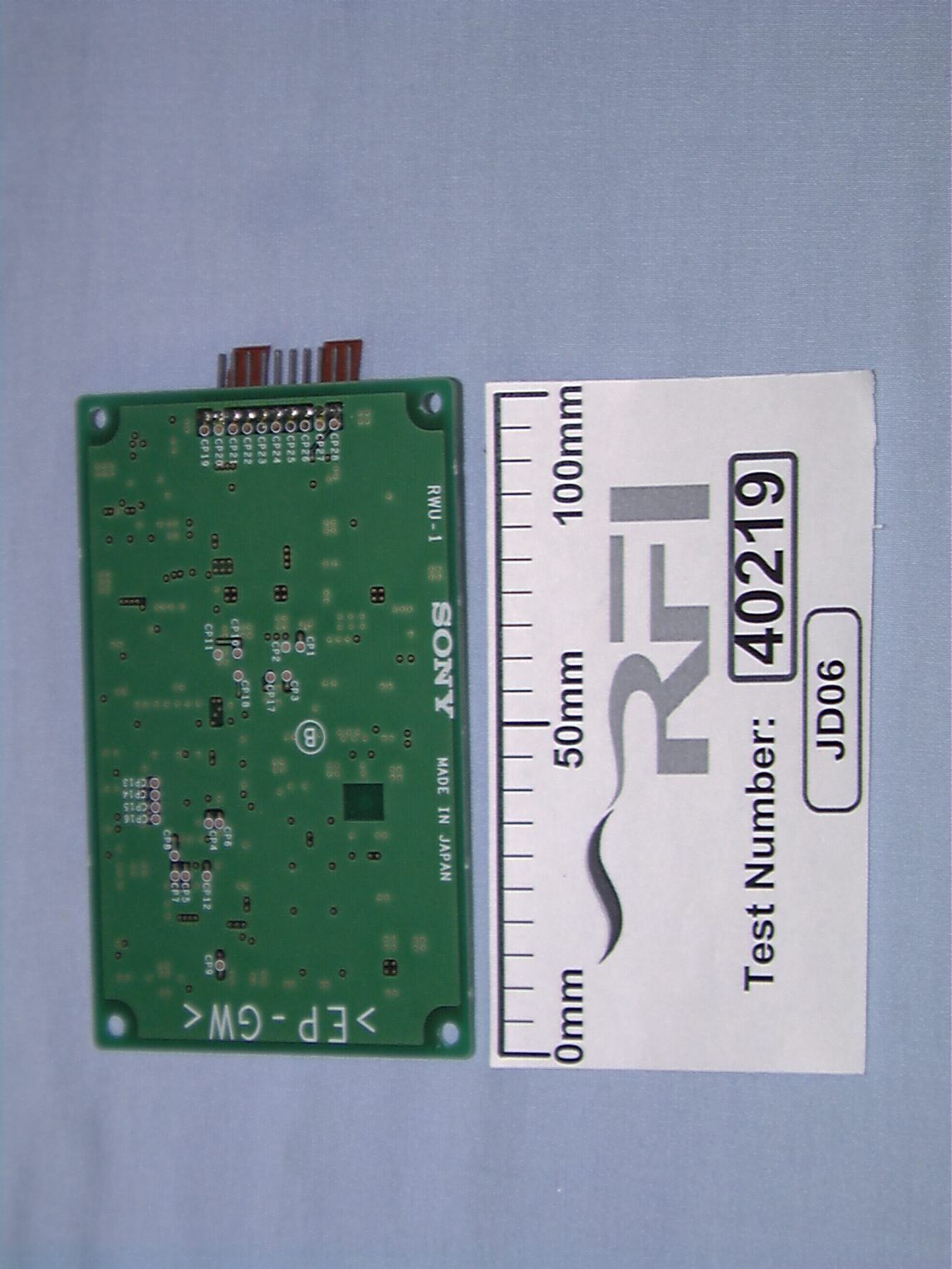
Radio Frequency Investigation Ltd, Ewhurst Park, Ramsdell, Basingstoke, Hampshire, RG26 5RQ, ENGLAND. Tel: +44 (0) 1256 851193 Fax: +44 (0) 1256 851192 Registered in England, No. 211 7901. Registered Office: Ewhurst Park, Ramsdell, Basingstoke, Hampshire RG26 5RQ TESTING 0644 TEST REPORT FROM RADIO FREQUENCY INVESTIGATION LTD. Test Of: Sony Corporation. RC-S430C Smart Card Reader To: FCC Part 15 Subpart C Clause 15.225: 1998 Test Report Serial No: RFI\EMCB1\RP40219C This Test Report Is Issued Under The Authority Of Brian Watson Technical Director: Checked By: Tested By:Release Version No: PDF01 Issue Date: 20 December 1999Test Date: 2 December to 16 December 1999 This report is issued in Adobe Acrobat portable document format (PDF). It is only a valid copy of the report if it is being viewed in PDF format with the following security options not allowed: Changing the document, Selecting text and graphics, Adding or changing notes and form fields. Furthermore, the date of creation must match the issue date stated above. This report may be copied in full. RADIO FREQUENCY INVESTIGATION LTD.TEST REPORT S.No: RFI\EMCB1\RP40219C EMC DepartmentPage 2 of 26 Issue Date: 20 December 1999 Test Of:Sony Corporation. RC-S430C Smart Card Reader To:FCC Part 15 Subpart C Clause 15.225: 1998 This page has been left intentionally blank. RADIO FREQUENCY INVESTIGATION LTD.TEST REPORT S.No: RFI\EMCB1\RP40219C EMC DepartmentPage 3 of 26 Issue Date: 20 December 1999 Test Of:Sony Corporation. RC-S430C Smart Card Reader To:FCC Part 15 Subpart C Clause 15.225: 1998 Table of Contents 1. Client Information......................................................................................................4 2. Equipment Under Test (EUT).....................................................................................5 3. Test Specification, Methods And Procedures..........................................................7 4. Deviations From The Test Specification...................................................................8 5. Operation Of The EUT During Testing......................................................................9 6. Summary Of Test Results........................................................................................10 7. Measurements, Examinations And Derived Results..............................................11 8. Measurement Uncertainty........................................................................................16 Appendix 1. Test Equipment Used...............................................................................17 Appendix 2. Measurement Methods............................................................................18 Appendix 3. Test Configuration Drawings..................................................................20 Appendix 4. Graphical Test Results............................................................................24 RADIO FREQUENCY INVESTIGATION LTD.TEST REPORT S.No: RFI\EMCB1\RP40219C EMC DepartmentPage 4 of 26 Issue Date: 20 December 1999 Test Of:Sony Corporation. RC-S430C Smart Card Reader To:FCC Part 15 Subpart C Clause 15.225: 1998 1. Client Information Company Name: Sony Corporation. Address: 6-7-35 Kitashinagawa Shinagawaku Tokyo 141-0001-Japan Contact Name: Mr. Toshimichi Okita. RADIO FREQUENCY INVESTIGATION LTD.TEST REPORT S.No: RFI\EMCB1\RP40219C EMC DepartmentPage 5 of 26 Issue Date: 20 December 1999 Test Of:Sony Corporation. RC-S430C Smart Card Reader To:FCC Part 15 Subpart C Clause 15.225: 1998 2. Equipment Under Test (EUT) The following information (with the exception of the Date of Receipt) has been supplied by the client: 2.1. Identification Of Equipment Under Test (EUT) Brand Name: Sony Model Name or Number: RC-S430C Unique Type Identification: None Stated by Client Serial Number: 32000842 Country of Manufacture: Japan FCC ID Number: Pending Date of Receipt: 2 December 1999 2.2. Description Of EUT The equipment under test is a smart card reader. 2.3. Modifications Incorporated In EUT The EUT has not been modified from what is described by the Model Name and Unique Type Identification stated above. 2.4. Additional Information Related To Testing Power Supply Requirement: Internal battery supply of + 12 V Intended Operating Environment: Residential and Commercial Weight: 0.5 kg Dimensions: 190 mm (L) x 125 mm (W) x 50 mm (H) Interface Ports: None RADIO FREQUENCY INVESTIGATION LTD.TEST REPORT S.No: RFI\EMCB1\RP40219C EMC DepartmentPage 6 of 26 Issue Date: 20 December 1999 Test Of:Sony Corporation. RC-S430C Smart Card Reader To:FCC Part 15 Subpart C Clause 15.225: 1998 2.5. Support Equipment The following support equipment was used to exercise the EUT during testing: Description: Smart Card (Support Tag) Brand Name: None Stated by Client Model Name or Number: None Stated by Client Serial Number: None Stated by Client FCC ID Number: None Stated by Client Cable Length And Type: No Direct Connection (Air link) Connected to Port: Not applicable RADIO FREQUENCY INVESTIGATION LTD.TEST REPORT S.No: RFI\EMCB1\RP40219C EMC DepartmentPage 7 of 26 Issue Date: 20 December 1999 Test Of:Sony Corporation. RC-S430C Smart Card Reader To:FCC Part 15 Subpart C Clause 15.225: 1998 3. Test Specification, Methods And Procedures 3.1. Test Specification Reference: FCC Part 15 Subpart C Clause 15.225: 1998 Title: Code of Federal Regulations, Part 15 (47CFR15) Radio Frequency Devices: Digital Devices. Comments: A description of the test facility used for this test is on file with, and has been accepted by, the Federal Communications Commission as required by Section 2.948 of Federal Rules. Purpose of Test: To determine whether the equipment complied with the applicable requirements of the specification for the purposes of certification. 3.2. Methods And Procedures The methods and procedures used were as detailed in: ANSI C63.2 (1987) Title: American National Standard for Instrumentation - Electromagnetic noise and field strength. ANSI C63.4 (1992…
Text truncated - open the document above for the full version.
Contact Information
Applicant
Kazuyuki Hori(Chief EMC/RF Compliance Specialist)
Technical Contact
Radio Frequency Investigation LtdNick G COBB
[email protected]+44 1256 855472
EWhurst Park, Ramsdell · Hampshire · United Kingdom
Technical Specifications
| # | Rule Parts | Frequency Range | Power Output |
|---|---|---|---|
| 1 | 15C | 13.56 MHz - 13.56 MHz | - |
Other Applications from Sony Group Corporation
AK8WW81782
Aug 21, 2026Radio Equipment
Equipment Class
DSS - Part 15 Spread Spectrum TransmitterAK8CFIZCP2
Aug 03, 2026Wireless Controller
Equipment Class
DSS - Part 15 Spread Spectrum TransmitterAK8OEV321MUH
Apr 14, 2026LCD Monitor
Equipment Class
JAD - Part 15 Class A Digital DeviceAK8OEV431MUH
Apr 14, 2026LCD Monitor
Equipment Class
JAD - Part 15 Class A Digital DeviceAK8OEV271MUH
Apr 14, 2026LCD Monitor
Equipment Class
JAD - Part 15 Class A Digital Device