AK8SEDE1SmartEyeglass
Sony Group Corporation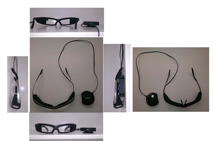
Click to zoom
Application Details
- Equipment Class
- DSS - Part 15 Spread Spectrum Transmitter
- Date of Grant
- Feb 01, 2015
- Application Purpose
- Original Equipment
- Date of Application
- Jan 29, 2015
- Equipment Note
- SmartEyeglass
- Frequency Range
- 2402.00000000 - 2480.00000000
- Company
- Sony Group Corporation
- Country
- Japan
Documents & Files
Document Text
Text extracted from the exhibit documents filed with the FCC. Open a document above to read the original.
Users Manual
SED-E1 U (US) 4-541-087-11(2) Manuals Startup Guide Read this guide first. Describes initial preparation such as charging and connecting. Reference Guide (this manual) Describes safety precautions or specifications. Help Guide Provides details about the device’s function or how to use the device. Help Guide is available on a smartphone or computer. http://rd1.sony.net/help/sed/sede1/ja/ Before operating the device, please read this guide thoroughly and retain it for future reference. Owner’s Record The serial number is located under the clip on the rear of the controller. Record the serial number in the space provided below. Refer to them whenever you call upon your Sony dealer regarding this product. Model No. SED-E1 Serial No. For customers in the USA Please register this product on line at http://www.sony.com/productregistration Proper registration will enable us to send you periodic updates about new products, services and other important announcements. Registering your product will also allow us to contact you in the unlikely event that the product needs adjustment or modification. Thank you. CAUTION This device complies with part 15 of the FCC Rules. Operation is subject to the following two conditions: (1) This device may not cause harmful interference, and (2) this device must accept any interference received, including interference that may cause undesired operation. You are cautioned that any changes or modifications not expressly approved in this manual could void your authority to operate this equipment. NOTE: This equipment has been tested and found to comply with the limits for a Class B digital device, pursuant to Part 15 of the FCC Rules. These limits are designed to provide reasonable protection against harmful interference in a residential installation. This equipment generates, uses and can radiate radio frequency energy and, if not installed and used in accordance with the instructions, may cause harmful interference to radio communications. However, there is no guarantee that interference will not occur in a particular installation. If this equipment does cause harmful interference to radio or television reception, which can be determined by turning the equipment off and on, the user is encouraged to try to correct the interference by one or more of the following measures: Reorient or relocate the receiving antenna. Increase the separation between the equipment and receiver. Connect the equipment into an outlet on a circuit different from that to which the receiver is connected. Consult the dealer or an experienced radio/TV technician for help. This equipment must not be co-located or operated in conjunction with any other antenna or transmitter. The available scientific evidence does not show that any health problems are associated with using low power wireless devices. There is no proof, however, that these low power wireless devices are absolutely safe. Low power Wireless devices emit low levels of radio frequency energy (RF) in the microwave range while being used. Whereas high levels of RF can produce health effects (by heating tissue), exposure of low-level RF that does not produce heating effects causes no known adverse health effects. Many studies of low-level RF exposures have not found any biological effects. Some studies have suggested that some biological effects might occur, but such findings have not been confirmed by additional research. SmartEyeglass (SED-E1) has been tested and found to comply with FCC radiation exposure limits set forth for an uncontrolled environment and meets the FCC radio frequency (RF) Exposure Guidelines. This SmartEyeglass (SED-E1) has been tested and meets the FCC RF exposure guidelines when used with the Sony Corporation accessories supplied or designated for this product. Use of other accessories may not ensure compliance with FCC RF exposure guidelines. Observe the following cautions, as there may be a risk of heat generation, fire, or explosion. *Lithium-ion battery is built into the product. Charge the product by the designated charging method. Do not place the product in or near fire, or put the product in a microwave. Do not leave the product in a car in hot weather. Do not store or use the product in a hot and humid place such as in a sauna bath. Do not disassemble, crush or pierce the product. Do not expose the product to excessive shock such as dropping from a high place. Do not expose the product to high temperatures above 60 °C (140 °F). Keep the product dry. Dispose of the product appropriately. Charge the product by the designated charging method in the instruction manual. If the battery pack is mishandled, the battery pack can burst, cause a fire or even chemical burns. Observe the following cautions. Do not disassemble. Do not crush and do not expose the battery pack to any shock or force such as hammering, dropping or stepping on it. Do not short circuit and do not allow metal objects to come into contact with the battery terminals. Do not expose to high temperature above 60 °C (140 °F) such as in direct sunlight or in a car parked in the sun. Do not incinerate or dispose of in fire. Do not handle damaged or leaking lithium ion batteries. Do not replace the battery with an incorrect type. Keep the battery pack out of the reach of small children. Keep the battery pack dry. Dispose of used battery packs promptly as described in the instructions. RECYCLING LITHIUM-ION BATTERIES Lithium-Ion batteries are recyclable. You can help preserve our environment by returning your used rechargeable batteries to the collection and recycling location nearest you. For more information regarding recycling of rechargeable batteries, call toll free 1-800-822-8837, or visit http://www.rbrc.org/ Caution: Do not handle damaged or leaking Lithium-Ion batteries. For the state of California, USA only Perchlorate Material - special handling may apply, See www.dtsc.ca.gov/hazardouswaste/perchl…
Text truncated - open the document above for the full version.
Cover Letter(s)
Sony EMCS Corporation Letter of Authorization Date: December 23, 2014 UL Japan, Inc. 4383-326 Asama-cho, Ise-shi, Mie 516-0021 Japan FCC ID : AK8SEDE1 Applicant : Sony Corporation To whom it may concern: Please be advised we authorize Yoshihisa Maeda of Consumer Technology Division, UL Japan, Inc. to act on our behalf, until otherwise notified, for applications submitted for Federal Communication Commission Radio equipment applications submitted to UL Japan, Inc. We certify that we are not subject to denial of federal benefits, t hat includes FCC benefits, pursuant to Section 5301 of the Anti-Drug Abuse ACT of 1988, U.S.C. 862. Further, no party, as defined in 47 CFR 1.2002(b), to the application is subject to denial of federal benefits, that includes FCC benefits. The application for the subject equipment has not been submitted to another TCB for certification. Thank you for your attention to this matter. Sincerely, Hideo Nomura Sony EMCS Corporation Product Safety Section 1, Quality Assurance Department 3 Telephone +81-50-3369-5593 Fax +81-587-36-8570
Cover Letter(s)
Sony EMCS Corporation Request for Confidentiality Date: December 23, 2014 UL Japan, Inc. 4383-326 Asama-cho, Ise-shi, Mie 516-0021 Japan FCC ID : AK8SEDE1 Applicant : Sony Corporation To whom it may concern: Please be advised that the following information is to be held confidential on behalf of us, referring to the FCC rules 0.457 and 0.459: Block Diagram Theory of Operation Schematics The application contains technical information which we deem to be trade secrets and proprietary. If made public, the information might be used to the disadvantage of the applicant in the market place. Thank you for your attention to this matter. Sincerely, Hideo Nomura Sony EMCS Corporation Product Safety Section 1, Quality Assurance Department 3 Telephone +81-50-3369-5593 Fax +81-587-36-8570
Cover Letter(s)
Sony EMCS Corporation Request for Short-Term Confidentiality Date: December 23, 2014 UL Japan, Inc. 4383-326 Asama-cho, Ise-shi, Mie 516-0021 Japan FCC ID : AK8SEDE1 Applicant : Sony Corporation To whom it may concern: Please be advised that the following information is to be held in confidence for 180 days from the date of the Grant of Equipment Authorization and behalf of us, referring to the FCC rules 0.457 and 0.459: External Photos Internal Photos Test Setup Photos User Manual The application contains technical information, which we deem to be trade secrets and proprietary. If made public, the information might be used to the disadvantage of the applicant in the market place. Thank you for your attention to this matter. Sincerely, ____________________________________ Hideo Nomura Sony EMCS Corporation Product Safety Section 1, Quality Assurance Department 3 Telephone +81-50-3369-5593 Fax +81-587-36-8570
External Photos
SED ‐ E1 External Photos
Internal Photos
RF Module ※ Shield Case Removed ( below ) Chip Antenna Internal photo SED ‐ E1 Board A ‐ side Board B ‐ side RF Module exists at reverse side of Board B ‐ side. SED ‐ E1 Internal Photos
RF Exposure Info
Test report No. : 10559367H-R1 Page : 1 of 69 FCC ID : AK8SEDE1 Issued date : January 20, 2015 Revised date : January 28, 2015 UL Japan, Inc. Ise EMC Lab. 4383-326 Asama-cho, Ise-shi, Mie-ken 516-0021 JAPAN Telephone: +81 596 24 8999 Facsimile: +81 596 24 8124 13-EM-F0429 SAR TEST REPORT Test Report No. : 10559367H-R1 Applicant :Sony Corporation Type of Equipment :SmartEyeglass Model No. :SED-E1 FCC ID : AK8SEDE1 Test regulation : FCC47CFR 2.1093 Test Result : Complied Reported SAR(1g) Value The highest reported SAR(1g) WLAN 11b/g/n 2.4GHz Body-worn : 0.457W/kg 1. This test report shall not be reproduced in full or partial, without the written approval of UL Japan, Inc. 2. The results in this report apply only to the sample tested. 3. This sample tested is in compliance with the limits of the above regulation. 4. The test results in this report are traceable to the national or international standards. 5. This test report must not be used by the customer to claim product certification, approval, or endorsement by NVLAP, NIST, or any agency of the Federal Government. 6. This test report covers SAR technical requirements. It does not cover administrative issues such as Manual or non-SAR test related Requirements. (if applicable) 7. This report is a revised version of 10559367H. 10559367H is replaced with this report. Date of test: January 8, 2015 Representative test engineer: Hisayoshi Sato Engineer Consumer Technology Division Approved by : Takahiro Hatakeda Leader Consumer Technology Division NVLAP LAB CODE: 200572-0 This laboratory is accredited by the NVLAP LAB CODE 200572-0, U.S.A. The tests reported herein have been performed in accordance with its terms of accreditation. *As for the range of Accreditation in NVLAP, you may refer to the WEB address, http://www.ul.com/japan/jpn/pages/services/emc/about/m ark1/index.jsp#nvlap Test report No. : 10559367H-R1 Page : 2 of 69 FCC ID : AK8SEDE1 Issued date : January 20, 2015 Revised date : January 28, 2015 UL Japan, Inc. Ise EMC Lab. 4383-326 Asama-cho, Ise-shi, Mie-ken 516-0021 JAPAN Telephone: +81 596 24 8999 Facsimile: +81 596 24 8124 REVISION HISTORY Original Test Report No.: 10559367H Revision Test report No. Date Page revised Contents - (Original) 10559367H January 20, 2015 - - 1 10559367H-R1 January 28, 2015 P. 1 Correction of Reported SAR(1g) Value of Cover 1 10559367H-R1 January 28, 2015 P. 7 Correction of Stand-alone SAR result of Clause 4.1 1 10559367H-R1 January 28, 2015 P. 14, 15 Correction of Standalone SAR test exclusion considerations Clause 6.1. 1 10559367H-R1 January 28, 2015 P. 16 Correction of Test position for Body-worn setup Clause 7.1. 1 10559367H-R1 January 28, 2015 P. 19 Correction of WLAN Body-worn SAR (2.4G) (3) Clause 9.1. 1 10559367H-R1 January 28, 2015 P. 24 to 28Addition of SAR Measurement data in Appendix 1. 1 10559367H-R1 January 28, 2015 P. 60, 62, 65 to 69 Addition of Photographs of test setup in Appendix 4. Test report No. : 10559367H-R1 Page : 3 of 69 FCC ID : AK8SEDE1 Issued date : January 20, 2015 Revised date : January 28, 2015 UL Japan, Inc. Ise EMC Lab. 4383-326 Asama-cho, Ise-shi, Mie-ken 516-0021 JAPAN Telephone: +81 596 24 8999 Facsimile: +81 596 24 8124 CONTENTS PAGE SECTION 1: Customer information ................................................................................................... 4 SECTION 2: Equipment under test (E.U.T.) ..................................................................................... 4 2.1 Identification of E.U.T. ....................................................................................................................................... 4 2.2 Product description ............................................................................................................................................. 4 SECTION 3 : Test standard information............................................................................................ 5 3.1 Test Specification ............................................................................................................................................... 5 3.2 Procedure ............................................................................................................................................................ 5 3.3 Exposure limit ..................................................................................................................................................... 6 3.4 Test Location ...................................................................................................................................................... 6 SECTION 4 : Test result ...................................................................................................................... 7 4.1 Stand-alone SAR result ....................................................................................................................................... 7 SECTION 5 : Description of the operating mode .............................................................................. 8 5.1 Output power operating modes ........................................................................................................................... 8 5.2 Output power measurement results ..................................................................................................................... 9 5.3 SAR testing operating modes.............................................................................................................................. 11 5.4 Confirmation after SAR testing .......................................................................................................................... 13 SECTION 6 SAR test exclusion considerations .................................................................................. 14 6.1 Standalone SAR test exclusion considerations ................................................................................................... 14 SECTION 7: De…
Text truncated - open the document above for the full version.
Test Report
Project No: JB-Z0036-F Model No.: SED-E1 FCC ID: AK8SEDE1 Issued: February 02, 2015 Page 2 of 73 Sony EMCS EMC/RF Test Laboratory Main Lab. A2LA Cert. #3203.01 Kisarazu Site 8-4 Shiomi Kisarazu-shi, Chiba, 292-0834 Japan PHONE +81-(438) 37-2750 FAX +81-(438) 37-2048 TABLE OF CONTENTS 1. General Information .................................................................................................................................................... 3 1.1. Description of Equipment Under Test (EUT) ...................................................................................................... 3 1.2. Summary of Test Result ......................................................................................................................................... 3 1.3. Tested Methodology ................................................................................................................................................ 4 1.4. Measurement Procedures ...................................................................................................................................... 4 1.5. Test Facility .............................................................................................................................................................. 7 1.6. Uncertainty .............................................................................................................................................................. 7 2. System Test Configuration .......................................................................................................................................... 8 2.1. Validation ................................................................................................................................................................. 8 2.2. Test Operating Conditions ..................................................................................................................................... 8 2.3. Special Accessories .................................................................................................................................................. 8 2.4. EUT Modifications .................................................................................................................................................. 8 2.5. Configuration of Tested System ............................................................................................................................ 9 3. Test Data ..................................................................................................................................................................... 10 3.1. AC Power-line Conducted Emissions ................................................................................................................. 10 3.2. 20dB Bandwidth .................................................................................................................................................... 11 3.3. Carrier Frequency Separation ............................................................................................................................. 13 3.4. Number of Hopping Frequencies ........................................................................................................................ 14 3.5. Time of Occupancy (Dwell Time) ......................................................................................................................... 15 3.6. Maximum Peak Conducted Output Power ........................................................................................................ 18 3.7. Radiated Spurious Emissions .............................................................................................................................. 19 3.8. Conducted Spurious Emissions for Band Edge ................................................................................................. 67 4. Method of Calculation ................................................................................................................................................ 68 5. List of Test Equipment .............................................................................................................................................. 70 5.1. AC Power-line Conducted Emissions ................................................................................................................. 70 5.2. Antenna-port Conducted Measurements ........................................................................................................... 70 5.3. Radiated Spurious Emissions .............................................................................................................................. 70 6. Photographs of test setup .......................................................................................................................................... 71 6.1. AC Power-line Conducted Emissions Measurement Photo(s) ........................................................................ 71 6.2. Antenna-port Conducted Measurements Photo(s) ........................................................................................... 71 6.3. Radiated Spurious Emissions Measurement Photo(s) ..................................................................................... 72 Note -indicates that be listed condition, standard or equipment is applicable for this report. -indicates that be listed condition, standard or equipment is not applicable for this report. Project No: JB-Z0036-F Model No.: SED-E1 FCC ID: AK8SEDE1 Issued: February 02, 2015 Page 3 of 73 Sony EMCS EMC/RF Test Laboratory Main Lab. A2LA Cert. #3203.01 Kisarazu Site 8-4 Shiomi Kisarazu-shi, Chiba, 292-0834 Japan PHONE +81-(438) 37-2750 FAX +81-(438) 37-2048 1. General Information 1.1. Description of Equipment Under Test (EUT) General specification Test Sample Condition : Prototype Pre-production Mass-production Type of Equipment : Sma…
Text truncated - open the document above for the full version.
Test Setup Photos
Test report No. : 10559367H-R1 Page : 59 of 69 FCC ID : AK8SEDE1 Issued date : January 20, 2015 Revised date : January 28, 2015 UL Japan, Inc. Ise EMC Lab. 4383-326 Asama-cho, Ise-shi, Mie-ken 516-0021 JAPAN Telephone: +81 596 24 8999 Facsimile: +81 596 24 8124 APPENDIX 4: Photographs of test setup 1. Photographs of EUT Right back view of transceiver Left front view of transceiver Whole view of EUT When an operator of this SAR test establishes a WLAN continuous transmission mode, this connector, Jig and PC are connected. When coming onto the market, there are no this connector. Test report No. : 10559367H-R1 Page : 60 of 69 FCC ID : AK8SEDE1 Issued date : January 20, 2015 Revised date : January 28, 2015 UL Japan, Inc. Ise EMC Lab. 4383-326 Asama-cho, Ise-shi, Mie-ken 516-0021 JAPAN Telephone: +81 596 24 8999 Facsimile: +81 596 24 8124 Each side of transceiver Front Rear Left side Right side Top side Bottom side Direction of Antenna side WLAN antenna Test report No. : 10559367H-R1 Page : 61 of 69 FCC ID : AK8SEDE1 Issued date : January 20, 2015 Revised date : January 28, 2015 UL Japan, Inc. Ise EMC Lab. 4383-326 Asama-cho, Ise-shi, Mie-ken 516-0021 JAPAN Telephone: +81 596 24 8999 Facsimile: +81 596 24 8124 Body-worn Body-worn 1 Around the clothes which are around the chest by a clip in the back of this transceiver. Body-worn 2 T his transceiver was put in a pocket around the chest. Test report No. : 10559367H-R1 Page : 62 of 69 FCC ID : AK8SEDE1 Issued date : January 20, 2015 Revised date : January 28, 2015 UL Japan, Inc. Ise EMC Lab. 4383-326 Asama-cho, Ise-shi, Mie-ken 516-0021 JAPAN Telephone: +81 596 24 8999 Facsimile: +81 596 24 8124 2. Antenna position Front Rear Right side Left side Bottom Top side Top side Bottom side WLAN antenna WLAN antenna <Front view> <Right side view > 3.56 mm Test report No. : 10559367H-R1 Page : 63 of 69 FCC ID : AK8SEDE1 Issued date : January 20, 2015 Revised date : January 28, 2015 UL Japan, Inc. Ise EMC Lab. 4383-326 Asama-cho, Ise-shi, Mie-ken 516-0021 JAPAN Telephone: +81 596 24 8999 Facsimile: +81 596 24 8124 3. Photographs of setup Front Test report No. : 10559367H-R1 Page : 64 of 69 FCC ID : AK8SEDE1 Issued date : January 20, 2015 Revised date : January 28, 2015 UL Japan, Inc. Ise EMC Lab. 4383-326 Asama-cho, Ise-shi, Mie-ken 516-0021 JAPAN Telephone: +81 596 24 8999 Facsimile: +81 596 24 8124 Rear Test report No. : 10559367H-R1 Page : 65 of 69 FCC ID : AK8SEDE1 Issued date : January 20, 2015 Revised date : January 28, 2015 UL Japan, Inc. Ise EMC Lab. 4383-326 Asama-cho, Ise-shi, Mie-ken 516-0021 JAPAN Telephone: +81 596 24 8999 Facsimile: +81 596 24 8124 Antenna Side Test report No. : 10559367H-R1 Page : 66 of 69 FCC ID : AK8SEDE1 Issued date : January 20, 2015 Revised date : January 28, 2015 UL Japan, Inc. Ise EMC Lab. 4383-326 Asama-cho, Ise-shi, Mie-ken 516-0021 JAPAN Telephone: +81 596 24 8999 Facsimile: +81 596 24 8124 Top Side Test report No. : 10559367H-R1 Page : 67 of 69 FCC ID : AK8SEDE1 Issued date : January 20, 2015 Revised date : January 28, 2015 UL Japan, Inc. Ise EMC Lab. 4383-326 Asama-cho, Ise-shi, Mie-ken 516-0021 JAPAN Telephone: +81 596 24 8999 Facsimile: +81 596 24 8124 Bottom Side Test report No. : 10559367H-R1 Page : 68 of 69 FCC ID : AK8SEDE1 Issued date : January 20, 2015 Revised date : January 28, 2015 UL Japan, Inc. Ise EMC Lab. 4383-326 Asama-cho, Ise-shi, Mie-ken 516-0021 JAPAN Telephone: +81 596 24 8999 Facsimile: +81 596 24 8124 Right Side Test report No. : 10559367H-R1 Page : 69 of 69 FCC ID : AK8SEDE1 Issued date : January 20, 2015 Revised date : January 28, 2015 UL Japan, Inc. Ise EMC Lab. 4383-326 Asama-cho, Ise-shi, Mie-ken 516-0021 JAPAN Telephone: +81 596 24 8999 Facsimile: +81 596 24 8124 Left Side End of Report
Test Setup Photos
Project No: JB-Z0036-F Model No.: SED-E1 FCC ID: AK8SEDE1 Issued: February 02, 2015 Page 71 of 73 Sony EMCS EMC/RF Test Laboratory Main Lab. A2LA Cert. #3203.01 Kisarazu Site 8-4 Shiomi Kisarazu-shi, Chiba, 292-0834 Japan PHONE +81-(438) 37-2750 FAX +81-(438) 37-2048 6. Photographs of test setup The following photographs show the arrangement of the worst case. 6.1. AC Power-line Conducted Emissions Measurement Photo(s) 6.2. Antenna-port Conducted Measurements Photo(s) Project No: JB-Z0036-F Model No.: SED-E1 FCC ID: AK8SEDE1 Issued: February 02, 2015 Page 72 of 73 Sony EMCS EMC/RF Test Laboratory Main Lab. A2LA Cert. #3203.01 Kisarazu Site 8-4 Shiomi Kisarazu-shi, Chiba, 292-0834 Japan PHONE +81-(438) 37-2750 FAX +81-(438) 37-2048 6.3. Radiated Spurious Emissions Measurement Photo(s) Below 30MHz 30 - 1000 MHz Above 1 GHz Project No: JB-Z0036-F Model No.: SED-E1 FCC ID: AK8SEDE1 Issued: February 02, 2015 Page 73 of 73 Sony EMCS EMC/RF Test Laboratory Main Lab. A2LA Cert. #3203.01 Kisarazu Site 8-4 Shiomi Kisarazu-shi, Chiba, 292-0834 Japan PHONE +81-(438) 37-2750 FAX +81-(438) 37-2048 <EUT Axis> X Y Z
Contact Information
Applicant
Kazuyuki Hori(Chief EMC/RF Compliance Specialist)
Technical Contact
UL Japan, Inc.Takahiro Hatakeda
[email protected]81-596-24-8999
4383-326 Asama-cho, Ise-shi · Mie-ken · Japan
Test Firm
UL Japan, Inc. Head office EMC Lab.Tetsuya Hashimoto
Technical Specifications
| # | Rule Parts | Frequency Range | Power Output |
|---|---|---|---|
| 1 | 15C | 2.40 GHz - 2.48 GHz | 1.40 mW |
Other Applications from Sony Group Corporation
AK8WW81782
Aug 21, 2026Radio Equipment
Equipment Class
DSS - Part 15 Spread Spectrum TransmitterAK8CFIZCP2
Aug 03, 2026Wireless Controller
Equipment Class
DSS - Part 15 Spread Spectrum TransmitterAK8OEV321MUH
Apr 14, 2026LCD Monitor
Equipment Class
JAD - Part 15 Class A Digital DeviceAK8OEV431MUH
Apr 14, 2026LCD Monitor
Equipment Class
JAD - Part 15 Class A Digital DeviceAK8OEV271MUH
Apr 14, 2026LCD Monitor
Equipment Class
JAD - Part 15 Class A Digital Device