AK8UPDX100Digital Photo Printer with Bluetooth
Sony Group Corporation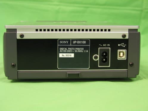
Click to zoom
Application Details
- Equipment Class
- DSS - Part 15 Spread Spectrum Transmitter
- Date of Grant
- Feb 25, 2003
- Application Purpose
- Original Equipment
- Date of Application
- Feb 25, 2003
- Equipment Note
- Digital Photo Printer with Bluetooth
- Frequency Range
- 2402.00000000 - 2480.00000000
- Company
- Sony Group Corporation
- Country
- Japan
Documents & Files
Document Text
Text extracted from the exhibit documents filed with the FCC. Open a document above to read the original.
External Photos
External Photo Sony Corporation Model: UP-DX100 FCC ID: AK8UPDX100 Front View Rear View External Photo Sony Corporation Model: UP-DX100 FCC ID: AK8UPDX100 Left Side View Right Side View External Photo Sony Corporation Model: UP-DX100 FCC ID: AK8UPDX100 Top View Bottom View External Photo Sony Corporation Model: UP-DX100 FCC ID: AK8UPDX100 Front View with Paper Tray
Internal Photos
Internal Photo Sony Corporation Model: UP-DX100 FCC ID: AK8UPDX100 Bluetooth Module (Front) Internal Photo Sony Corporation Model: UP-DX100 FCC ID: AK8UPDX100 Without front enclosure Internal Photo Sony Corporation Model: UP-DX100 FCC ID: AK8UPDX100 Right Side Open the cartridge compartment Cover Internal Photo Sony Corporation Model: UP-DX100 FCC ID: AK8UPDX100 Rear Side of Bluetooth Module Internal Photo Sony Corporation Model: UP-DX100 FCC ID: AK8UPDX100 Circuit Board (Front) Internal Photo Sony Corporation Model: UP-DX100 FCC ID: AK8UPDX100 Circuit Board (Back) Internal Photo Sony Corporation Model: UP-DX100 FCC ID: AK8UPDX100 Without top enclosure
Operational Description
Operational Description of UP-DX100 The digital photo printer UP-DX100 is a printer used in the digital printing system UPX-C200. By incorporating the Bluetooth radio module in UP-DX100, it transmits with the digital video camera DKC-C200X on the air, receives image data from DKC-C200X and prints out the image on a proper paper. The circuit blocks of UP-DX100 are as follow: [Outline Description of Each Block] -Main CPU Block -MA-123 Circuit Board >Load Digital Signal from Bluetooth/USB to main memory and after running with software, output to thermal head. >Mechanical Block Controlling >Controlling Bluetooth System/ USB Controlling >Memory (FLASH ROM, SDRAM, EEPROM) Controlling >Liquid crystal display/ Key input/ LED Controlling >3.3V/ 1.8V regulator [Mechanical Controlling Block] -MD-128 Circuit Board >Stepping Motor/ DC Motor Controlling >Ribbon Insertion/ Type Detection >Detect Head location >Controlling Buzzer/ Fan >5V Regulator [Other Blocks] -IF-908 Circuit Board >USB Interface Connector -JUM-5 Circuit Board >Paper Edge detection/ Paper Presence -PE-40 Circuit Board >Paper Edge detection/ Paper Presence -RM-194 Circuit Board >Ribbon Start Mark Detection -Thermal Head Block >Receive image data from MA-123 Circuit Board and print out the image. -Power Supply Block >Switching Regulator [Power Supply of Bluetooth Block] Circuits in the Bluetooth block use +3.3 V and +1.8 V. The regulated +3.3 V is generated by +5.0 V regulated power supply IC803 on the PCB board MD-128 . The 5.0 V is supplied from +22.0 V in the power supply block. The 3.3 V is supplied to the Bluetooth module on the PCB board MA-123 after filtering by L501. The regulated +1.8 is generated in the Bluetooth HIC and supplied to the radio part of the Bluetooth module. Functional Description 20/May/2002 MITSUMI Bluetooth Module “ WML-C09###” “ WML-C10###” Hardware: Version 1 Ultra-small and thin size achieved through use of high density mounting technology . 1. APPLICATIONS Notebook PCs, mobile phones, digital cameras, PC peripherals, PDA. 2. DESCRIPTIONS Wireless communication module conforming to Bluetooth Ver.1.1. 3. FEATURES 1) Ultra-small and thin size achieved through use of high density mounting technology. 2) SMD type can be surface mounted. 3) High sensitivity supports communications of up to 1 0 m. 4) UART, USB and PCMIF interfaces enable wide range of applications. 5) Conforms to FCC, CE and other countries’ EMI standards. 6) Supports Bluetooth Class2. Note) The BLUETOOTH trademarks are owned by Bluetooth SIG, INC.,U.S.A. 4. SPECIFICATIONS I t e mS p e c I f I c a t I o n s F r e q u e n c y 2402 to 2480 MHz M o d u l a t I o n FHSS / GFSK Channel intervals 1 MHz Number of channels 7 9 CH Power supply voltage 3.3 V (typ.), 2.8 ~ 3.4V Transmission rate7 2 1 kbps Receive sensitivity -80 dBm typ. Output level (Class2)4 dBm max. TM ©1998-2000 MITSUMI Electronics Corp. All rights reserved. MITSUMI is a trademark of MITSUMI Electronics Corporation. Other company names and products names are trademarks of their respective companies. Product specifications are subject to revisions or changes without notification. 5. TERMINAL DESCRIPTION 5-1. WML-C09### No.SymbolI/O Description 1GNDGround 2VDD1Voltage monitor (+1.8V) when voltage regulator is integrated, or Supply voltage 1.8V 3SPI_MISOOSynchronous Serial Interface data output 4SPI_CSBIChip select for Synchronous Serial Interface 5SPI_CLKISynchronous Serial Interface Clock 6SPI_MOSIISynchronous Serial Interface data input 7VDD2Supply voltage 3.3V 8GNDGround 9UART_CTSIAsynchronous serial data CTS 10UART_RTSOAsynchronous serial data RTS 11UART_TXOAsynchronous serial data output 12UART_RXIAsynchronous serial data input 13PCM_CLKI/OSynchronous PCM data clock 14PCM_INISynchronous PCM data input 15PCM_SYNCI/OSynchronous data strobe 16PCM_OUTOSynchronous PCM data out 17GNDGround 18USB_D+I/OUSB Data + 19USB_D-I/OUSB Data - 20PIO [2] / USB_PULL_UPI/OProgrammable I/O line / USB pull-up 21PIO [3] / USB_RESUMEI/OProgrammable I/O line / USB resume 22PIO [4]I/OProgrammable I/O line 23RSTIReset if high 24GNDGround 25ANTI/ORF input/output 26GNDGround 5-2. WML-C10### No.SymbolI/O Description 1GNDGround 2VDD1Voltage monitor (+1.8V) when voltage regulator is integrated, or Supply voltage 1.8 V 3RSTIReset if high 4AIO [1]I/OProgrammable I/O line 5SPI_MISOOSynchronous Serial Interface data output 6SPI_CSBIChip select for Synchronous Serial Interface 7SPI_CLKISynchronous Serial Interface Clock 8SPI_MOSIISynchronous Serial Interface data input 9VDD2Supply voltage 3.3V (Operating voltage for memory & AIO) 10GNDGround 11UART_CTSIAsynchronous serial data CTS 12UART_RTSOAsynchronous serial data RTS 13UART_TXOAsynchronous serial data output 14UART_RXIAsynchronous serial data input 15PCM_CLKI/OSynchronous PCM data clock 16PCM_INISynchronous PCM data input 17PCM_SYNCI/OSynchronous data strobe 18PCM_OUTOSynchronous PCM data out 19VDD3Supply voltage 3.3V (Operating voltage for PIO & all other Input / Output) 20GNDGround 21USB_D+I/OUSB Data + 22USB_D-I/OUSB Data - 23PIO [2] / USB_PULL_UPI/OProgrammable I/O line / USB pull-up 24PIO [5]I/OProgrammable I/O line 25PIO [6]I/OProgrammable I/O line 26PIO [3] / USB_RESUMEI/OProgrammable I/O line / USB resume 27PIO [8]I/OProgrammable I/O line 28PIO [4]I/OProgrammable I/O line 29PIO [7]I/OProgrammable I/O line 30GNDGround 31ANTI/ORF input/output 32GNDGround 6. BLOCK DIAGRAM 6-1.WML-C09### 6-2.WML-C10### UART USB_D+ USB_D- UART_TX UART_RX UART_RTS UART_CTS SPI_CSB SPI_CLK SPI_MOSI SPI_MISO PCM_OUT PCM_IN PCM_SYNC PCM_CLK SPI PCM/IF MEMORY DRIVER FLASH ROM (256kx16) RAM RF Receiver RF Transmitter 1st Synthesizer Baseband- Controller Memory- Management 2 nd Synthesizer REG 16bits Micro- Processor XT Driver 16MHzVDD1 ANT BPF BC2-UART / BC2-USB Balun PIO [2],...,PIO [4] USB Programmable P/O VDD2 UART USB_D+ USB_D- UART_TX UART_RX UART_RTS UART_CTS SPI_CSB SPI_CLK SPI_MOSI SPI_MISO PCM_OUT PCM_IN PCM_SYNC PCM_CLK SPI PCM/IF MEMORY DRIVER FLASH ROM (256kx16) RAM RF Rece…
Text truncated - open the document above for the full version.
RF Exposure Info
RF Exposure Statement No. : 23BE0019-HO-10 Applicant : Sony Corporation Type of Equipment : Digital Photo Printer Model No. : UP-DX100 FCC ID : AK8UPDX100 A-Pex International Co., Ltd. EMC Head Office Division. 4383-326 Asama-cho, Ise-shi, Mie-ken 516-0021 JAPAN Telephone : +81 596 24 8116 Facsimile : +81 596 24 8124 RF Exposure Statement: Sony Corporation declares that Model : UP-DX100complies with FCC radiation exposure requirement specified in the FCC Rules 2.1093(2). UP-DX100 has 0.724mW of conducted Peak output power and 1.643mW of EIRP.(Antenna gain : 3.56dBi) According to RF output power of this module transmitter, values for both Conducted peak output power and EIRP are below 5mW.This kind of equipment hardly ever go over SAR value limited of 1.6W/Kg for public resident which is regulated by "OET Bulletin65, Supplement C". RF Exposure Calculations: The following information provides the minimum separation distance for the highest gain antenna provided with the “UP-DX100” as calculated from FCC OET 65 Appendix B, Table (B) Limits for General Population / Uncontrolled Exposure. This calculation is based on the highest EIRP possible from the system, considering maximum power and antenna gain, and considering a 1.0m W/cm^2 uncontrolled exposure limit. The Friis formula used was: S = (P * G) / (4* * r^2) or r = (P * G) / (4 * * S) Where S = 1.0 mW/cm^2 for 2400 MHz P = 0.724mW(Maximum Conducted Power) G =2.27 (Numerical Antenna gain; equal to 3.56 dBi) r = Minimum safe distance from antenna (cm) For: UP-DX100 r = 0.36cm Notes in Installation Manual: FCC Radiated Exposure Statement: This module may be installed into any end product both mobile and portable applications. Because the module only radiates very low power levels, it complies with RF exposure requirements. According to Supplement C, Edition 01-01 to OET Bulletin 65, Edition 97-01 spread spectrum transmitters are categorically excluded from routine environmental evaluation because of the low power level, where there is a high likelihood of compliance with RF exposure standards.
Test Report
Test report No. : 23BE0019-HO-10 Page : 2 of 56 Issued date : January 23, 2003 FCC ID : AK8UPDX100 A-Pex International Co., Ltd. EMC Head Office Division. 4383-326 Asama-cho, Ise-shi, Mie-ken 516-0021 JAPAN Telephone: +81 596 24 8116 Facsimile: +81 596 24 8124 CONTENTS PAGE SECTION 1: Client information 3 SECTION 2: Equipment under test (E.U.T.) 3 SECTION 3: Test specification, procedures and results 5 SECTION 4: Operation of E.U.T. during testing 7 SECTION 5: Conducted Emission, Section 15.207 9 SECTION 6: Carrier Frequency Separation, Section 15.247 (a)(1) 9 SECTION 7: 20dB Bandwidth , Section 15.247(a)(1) 10 SECTION 8: Number of Hopping Frequency, Section 15.247(a)(1)(iii) 10 SECTION 9: Dwell time, Section 15.247(a)(1)(iii) 10 SECTION 10: Maximum Peak Output Power, Section 15.247(b)(1) 10 SECTION 11: Band Edge Compliance, Section 15.247(c) 11 SECTION 12: Spurious Emission, Section 15.247(c) 11 APPENDIX 1: Photographs of test setup 12 APPENDIX 2: Test instruments 12 APPENDIX 3: Data of EMI test 12 Test report No. : 23BE0019-HO-10 Page : 5 of 56 Issued date : January 23, 2003 FCC ID : AK8UPDX100 A-Pex International Co., Ltd. EMC Head Office Division. 4383-326 Asama-cho, Ise-shi, Mie-ken 516-0021 JAPAN Telephone: +81 596 24 8116 Facsimile: +81 596 24 8124 SECTION 3: Test specification, procedures and results 3.1 Test Specification Test Specification : FCC Part 15 Subpart C Section 15.207 and Section15.247 Title : FCC 47CFR Part15 Radio Frequency Device Subpart C Intentional Radiators Section 15.207 Conducted emission limits; general requirements Section 15.247 Operation within the bands 902-928MHz, 2400-2483.5Mhz, 5725-5850MHz 3.2 Procedures and results No. Item Test Procedure Specification Remarks Deviation Worst margin Results 1 Conducted Emission ANSI C63.4:2001 Section 15.207 N/A N/A 8.6dB 0.1808MHz, L1 Complied 2 Carrier Frequency Separation ANSI C63.4:2001 Section15.247(a)(1) Conducted N/A N/A Complied 3 20dB Bandwidth ANSI C63.4:2001 Section15.247(a)(1) Conducted N/A N/A Complied 4 Number of Hopping Frequency ANSI C63.4:2001 Section15.247(a)(1)(iii) Conducted N/A N/A Complied 5 Dwell time ANSI C63.4:2001 Section15.247(a)(1)(iii) Conducted N/A N/A Complied 6 Maximum Peak Output Power ANSI C63.4:2001 Section15.247(b)(1) Conducted N/A N/A Complied 7 Band Edge Compliance ANSI C63.4:2001 Section15.247(c) Conducted N/A N/A Complied 8 Spurious Emission ANSI C63.4:2001 Section15.247(c) Conducted / Radiated N/A 4.5dB 4804MHz Horizontal Complied These tests were also referred to FCC Public Notice DA 00-705 "Guidance on Measurement for Frequency Hopping Spread Spectrum Systems. 3.3 Additions to standards No addition, deviation or exclusion has been made from standards. 3.4 Confirmation A-Pex International Co., Ltd. hereby confirms that E.U.T. , in the configuration tested, complies with the specifications FCC Part15 Subpart C Section 15.207 and Section 15.247. Test report No. : 23BE0019-HO-10 Page : 6 of 56 Issued date : January 23, 2003 FCC ID : AK8UPDX100 A-Pex International Co., Ltd. EMC Head Office Division. 4383-326 Asama-cho, Ise-shi, Mie-ken 516-0021 JAPAN Telephone: +81 596 24 8116 Facsimile: +81 596 24 8124 3.5 Uncertainty Conducted Emission The measurement uncertainty (with a 95% confidence level) for this test was + 1.3dB. The data listed in this test report has enough margin, more than the site margin. Spurious Emission(Radiated) The measurement uncertainty (with a 95% confidence level) for this test using Biconical antenna is + 4.5dB. The measurement uncertainty (with a 95% confidence level) for this test using Logperiodic antenna is + 5.2dB. The measurement uncertainty (with a 95% confidence level) for this test using Horn antenna is + 6.6dB. The data listed in this test report may exceed the test limit because it does not have enough margin. Other test except Conducted Emission and Spurious Emission (Radiated) The measurement uncertainty (with a 95% confidence level) for this test was + 3.0dB. The data listed in this test report has enough margin. 3.6 Test Location A-Pex International Co., Ltd. EMC Head Office Division. No.1 semi anechoic chamber, 19.2 x 11.2 x 7.7m No.2 semi anechoic chamber 7.5 x 5.8 x 5.2 m. 4383-326 Asama-cho, Ise-shi, Mieken 516-0021 JAPAN Telephone: +81 596 24 8116 Facsimile: +81 596 24 8124 This site has been fully described in a report submitted to FCC office, and listed on February 01, 2002/June 05, 2002 (Registration number: 313583/846015) *NVLAP Lab. Code: 200572-0 3.7 Test setup, Data of EMI and Test instruments Refer to Appendix 1 to 3. Test report No. : 23BE0019-HO-10 Page : 7 of 56 Issued date : January 23, 2003 FCC ID : AK8UPDX100 A-Pex International Co., Ltd. EMC Head Office Division. 4383-326 Asama-cho, Ise-shi, Mie-ken 516-0021 JAPAN Telephone: +81 596 24 8116 Facsimile: +81 596 24 8124 SECTION 4: Operation of E.U.T. during testing 4.1 Operating Modes The EUT exercise program used during radiated testing was designed to exercise the various system components in a manner similar to typical use. The operating mode/system was as follows: Operation mode : Transmitting 1.Transmitting mode(2402 MHz) 2.Transmitting mode(2441 MHz) 3.Transmitting mode(2480MHz) 4.Transmitting mode(Hopping on) 5.Inquiry Justification: The system was configured in typical fashion (as a customer would normally use it) for testing. 4.2 Configuration and peripherals [Conducted emission and spurious Emission (Radiated)] UP-DX100 A: EUT B E C D 4 13 AC 120V/60Hz AC 120V/60Hz 1 AC 120V/60Hz F 15 11 14 12 10 9 * Cabling was taken into consideration and test data was taken under worst case conditions. Test report No. : 23BE0019-HO-10 Page : 8 of 56 Issued date : January 23, 2003 FCC ID : AK8UPDX100 A-Pex International Co., Ltd. EMC Head Office Division. 4383-326 Asama-cho, Ise-shi, Mie-ken 516-0021 JAPAN Telephone: +81 596 24 8116 Facsimile: +81 596 24 8124 [Other tests except Conducted Emission and Spurious Emission (Radiated)] UP-DX100 A: EUT AC 120V/60Hz 4 Description of EUT…
Text truncated - open the document above for the full version.
Test Setup Photos
Test report No. : 23BE0019-HO-10 Page : 13 of 56 Issued date : January 23, 2003 FCC ID : AK8UPDX100 A-Pex International Co., Ltd. EMC Head Office Division. 4383-326 Asama-cho, Ise-shi, Mie-ken 516-0021 JAPAN Telephone: +81 596 24 8116 Facsimile: +81 596 24 8124 APPENDIX 1: Photographs of test setup Conducted emission (UP-DX100) Test report No. : 23BE0019-HO-10 Page : 14 of 56 Issued date : January 23, 2003 FCC ID : AK8UPDX100 A-Pex International Co., Ltd. EMC Head Office Division. 4383-326 Asama-cho, Ise-shi, Mie-ken 516-0021 JAPAN Telephone: +81 596 24 8116 Facsimile: +81 596 24 8124 Spurious Emission (Radiated) (UP-DX100) Test report No. : 23BE0019-HO-10 Page : 15 of 56 Issued date : January 23, 2003 FCC ID : AK8UPDX100 A-Pex International Co., Ltd. EMC Head Office Division. 4383-326 Asama-cho, Ise-shi, Mie-ken 516-0021 JAPAN Telephone: +81 596 24 8116 Facsimile: +81 596 24 8124 Other tests except Conducted emission and Spurious Emission (Radiated) (UP-DX100)
Contact Information
Applicant
Kazuyuki Hori(Chief EMC/RF Compliance Specialist)
Technical Contact
A-Pex International Co., Ltd.Hiroka Umeyama
[email protected]81-596-24-8116
4383-326 Asama-cho, · Ise-shi, Mie-ken · Japan
Non-Technical Contact
A-Pex International Co., Ltd.Keijiro Kumagai
[email protected]81-596-24-8116
Test Firm
UL Apex Co., Ltd.Tetsuya Hashimoto
Technical Specifications
| # | Rule Parts | Frequency Range | Power Output |
|---|---|---|---|
| 1 | 15C | 2.40 GHz - 2.48 GHz | 724.00 µW |
Other Applications from Sony Group Corporation
AK8WW81782
Aug 21, 2026Radio Equipment
Equipment Class
DSS - Part 15 Spread Spectrum TransmitterAK8CFIZCP2
Aug 03, 2026Wireless Controller
Equipment Class
DSS - Part 15 Spread Spectrum TransmitterAK8OEV321MUH
Apr 14, 2026LCD Monitor
Equipment Class
JAD - Part 15 Class A Digital DeviceAK8OEV431MUH
Apr 14, 2026LCD Monitor
Equipment Class
JAD - Part 15 Class A Digital DeviceAK8OEV271MUH
Apr 14, 2026LCD Monitor
Equipment Class
JAD - Part 15 Class A Digital Device