AK8YY2960Wireless Gaming Headset
Sony Group Corporation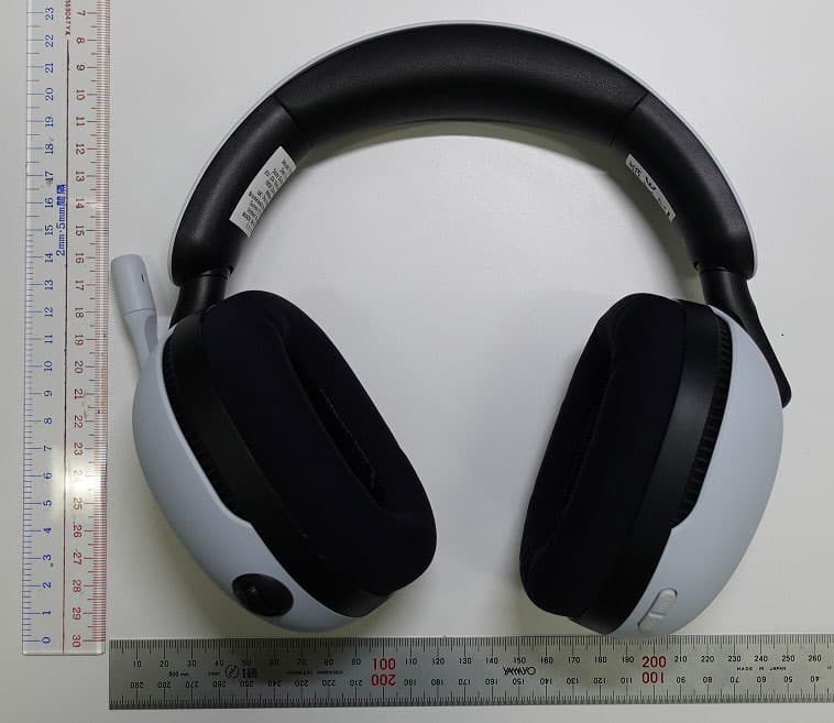
Click to zoom
Application Details
- Equipment Class
- DTS - Digital Transmission System
- Date of Grant
- Mar 21, 2022
- Application Purpose
- Original Equipment
- Date of Application
- Mar 21, 2022
- Equipment Note
- Wireless Gaming Headset
- Frequency Range
- 2402.00000000 - 2480.00000000
- Company
- Sony Group Corporation
- Country
- Japan
Documents & Files
Document Text
Text extracted from the exhibit documents filed with the FCC. Open a document above to read the original.
Users Manual
YY2959 / YY2960 (UC) [US/FR/ES] 5-038-201-12(1) Model, Modèle, Modelo: YY2959 / YY2960 Wireless Noise Canceling Gaming Headset (YY2959) Casque de jeu sans fil à réduction de bruit (YY2959) Wireless Gaming Headset (YY2960) Casque de jeu sans fil (YY2960) 5-038-201-12(1) Reference GuideGuide de référenceGuía de referencia ©2022 Sony Corporation Printed in Vietnam Imprimé au Vietnam https://www.sony.net/ https://rd1.sony.net/help/mdr/295960/h_zz/ English Wireless Noise Canceling Gaming Headset Wireless Gaming Headset Model: YY2959 / YY2960 FOR UNITED STATES CUSTOMERS. NOT APPLICABLE IN CANADA, INCLUDING IN THE PROVINCE OF QUEBEC. POUR LES CONSOMMATEURS AUX ÉTATS-UNIS. NON APPLICABLE AU CANADA, Y COMPRIS LA PROVINCE DE QUÉBEC. Owner’s Record The model and serial numbers are located on the product. Record them in the space below and store safely. Model No.________________________ Serial No._________________________ Do not install the product in a confined space, such as a bookcase or built-in cabinet. Do not expose the batteries (battery pack or batteries installed) to excessive heat, such as sunshine, fire or the like, for a long time. Do not subject the batteries to extreme low temperature conditions that may result in overheating and thermal runaway. Do not dismantle, open, or shred secondary cells or batteries. In the event of a cell leaking, do not allow the liquid to come in contact with the skin or eyes. If contact has been made, wash the affected area with copious amounts of water and seek medical advice. Secondary cells and batteries need to be charged before use. Always refer to the manufacturer’s instructions or product manual for proper charging instructions. After extended periods of storage, it may be necessary to charge and discharge the cells or batteries several times to obtain maximum performance. Dispose of properly. RECYCLING RECHARGEABLE BATTERIES Rechargeable batteries are recyclable. You can help preserve our environment by returning your used rechargeable batteries to the collection and recycling location nearest you. For more information regarding recycling of rechargeable batteries, visit http://www.sony. com/electronics/eco/environmental- management Caution: Do not handle damaged or leaking rechargeable batteries. FOR UNITED STATES CUSTOMERS. NOT APPLICABLE IN CANADA, INCLUDING IN THE PROVINCE OF QUEBEC. POUR LES CONSOMMATEURS AUX ÉTATS-UNIS. NON APPLICABLE AU CANADA, Y COMPRIS LA PROVINCE DE QUÉBEC. You are cautioned that any changes or modifications not expressly approved in this manual could void your authority to operate this unit. If you have any questions about this product: Visit: https://www.sony.com/electronics/ support Contact: Sony Customer Information Service Center at 1-800-222-7669 Write: Sony Customer Information Service Center 12451 Gateway Blvd., Fort Myers, FL 33913 Supplier’s Declaration of Conformity Trade Name: SONY Model: YY2959 / YY2960 Responsible Party: Sony Electronics Inc. Address: 16535 Via Esprillo, San Diego, CA 92127 U.S.A. Telephone Number: 858-942-2230 This device complies with Part 15 of the FCC Rules. Operation is subject to the following two conditions: (1) this device may not cause harmful interference, and (2) this device must accept any interference received, including interference that may cause undesired operation. NOTE: This unit has been tested and found to comply with the limits for a Class B digital device, pursuant to Part 15 of the FCC Rules. These limits are designed to provide reasonable protection against harmful interference in a residential installation. This unit generates, uses, and can radiate radio frequency energy and, if not installed and used in accordance with the instructions, may cause harmful interference to radio communications. However, there is no guarantee that interference will not occur in a particular installation. If this unit does cause harmful interference to radio or television reception, which can be determined by turning the unit off and on, the user is encouraged to try to correct the interference by one or more of the following measures: • Reorient or relocate the receiving antenna. •Increase the separation between the unit and r eceiver. •Connect the unit into an outlet on a circuit diff erent from that to which the receiver is connected. • Consult the dealer or an experienced radio/ TV t echnician for help. This unit must not be co-located or operated in conjunction with any other antenna or transmitter. This unit complies with FCC radiation exposure limits set forth for an uncontrolled environment and meets the FCC radio frequency (RF) Exposure Guidelines. This unit has very low levels of RF energy that is deemed to comply without testing of specific absorption rate (SAR). This conformity statement is only applicable to the YY2959/ YY2960. For customers in Canada This unit contains licence-exempt transmitter(s)/receiver(s) that comply with Innovation, Science and Economic Development Canada’s licence-exempt RSS(s). Operation is subject to the following two conditions: (1) This unit may not cause interference; and (2) This unit must accept any interference, including interference that may cause undesired operation of the unit. The available scientific evidence does not show that any health problems are associated with using low power wireless devices. There is no proof, however, that these low power wireless devices are absolutely safe. Low power wireless devices emit low levels of radio frequency energy (RF) in the microwave range while being used. Whereas high levels of RF can produce health effects (by heating tissue), exposure of low-level RF that does not produce heating effects causes no known adverse health effects. Many studies of low-level RF exposures have not found any biological effects. Some studies have suggested that some biological effects might occur, but such findings have not been confirmed by additional research. The unit has been tested and found to comply with ISED …
Text truncated - open the document above for the full version.
Cover Letter(s)
Sony Global Manufacturing & Operations Corporation Letter of Authorization Date: February 4, 2022 UL Verification Services Inc. 47173 Benicia Street, Fremont, CA 94538 Applicant: Sony Group Corporation FCC ID: AK8YY2960 To whom it may concern: We, the undersigned, hereby authorize Akiko Nishimura of Consumer, Medical & Information Technologies Division, UL Japan, Inc. to act on our behalf in all manners relating to application for equipment authorization, including signing of all documents relating to these matters. Any and all acts carried out by UL Japan, Inc. on our behalf shall have the same effect as acts of our own. We, the undersigned, hereby certify that we are not subject to a denial of federal benefits, that includes FCC benefits, pursuant to Section 5301 of the Anti-Drug Abuse Act of 1988, 21 U.S.C. 862. This authorization is valid until further written notice from the applicant. The application for the subject equipment has not been submitted to another TCB for certification. Sincerely Yours, Hideo Nomura Sony Global Manufacturing & Operations Corporation
Cover Letter(s)
Sony Global Manufacturing & Operations Corporation Request for Confidentiality Date: February 4, 2022 UL Verification Services Inc. 47173 Benicia Street, Fremont, CA 94538 Applicant : Sony Group Corporation FCC ID : AK8YY2960 To whom it may concern: Please be advised that the following information is to be held confidential on behalf of us, referring to the FCC rules 0.457 and 0.459: Block Diagram Theory of Operation Schematics Parts List The application contains technical information which we deem to be trade secrets and proprietary. If made public, the information might be used to the disadvantage of the applicant in the market place. Thank you for your attention to this matter. Sincerely, Hideo Nomura Sony Global Manufacturing & Operations Corporation
Cover Letter(s)
Sony Global Manufacturing & Operations Corporation Request for Short-Term Confidentiality Date: February 4, 2022 UL Verification Services Inc. 47173 Benicia Street, Fremont, CA 94538 FCC ID : AK8YY2960 Applicant : Sony Group Corporation To whom it may concern: Please be advised that the following information is to be held in confidence for 180 days from the date of the Grant of Equipment Authorization and behalf of us, referring to the FCC rules 0.457 and 0.459: External Photos Internal Photos Test Setup Photos User Manual The application contains technical information, which we deem to be trade secrets and proprietary. If made public, the information might be used to the disadvantage of the applicant in the market place. Thank you for your attention to this matter. Sincerely, ____________________________________ Hideo Nomura Sony Global Manufacturing & Operations Corporation
Cover Letter(s)
Sony Group Corporation Special Power of Attorney I, Kazuyuki Hori of Sony Group Corporation, hereby appoint Hideo Nomura of Sony Global Manufacturing & Operations Corporation to represent me to act on my behalf to do any and all of the following. Sign on my behalf the agency, anti-drug and confidentiality cover letters and apply to FCC for the products. The rights, powers and authority in fact to exercise any and all of the rights and powers herein granted shall commence and be in full force from April 1, 2021 and continue to be effective unless specifically terminated by either party. Dated April 1, 2021 Kazuyuki Hori Company: Sony Group Corporation Country: Japan
External Photos
付帯項目 Sony Corporation YY2960 External Photo 2021.12.13 付帯項目部署名ライツ表記日付 2 FrontRear 付帯項目部署名ライツ表記日付 3 RightLeftTo p Bottom 付帯項目部署名ライツ表記日付 4 EOF
ID Label/Location Info
R side L side Thereis thenameplateinsideofL side * FCC ID height:1.5mm
Internal Photos
付帯項目 Sony Corporation YY2960 Internal Photo 2021.12.20 付帯項目部署名ライツ表記日付 2 L side R side 付帯項目部署名ライツ表記日付 3 EOF
Internal Photos
付帯項目 Sony Corporation YY2960 PWB Photo 2022.02.21 付帯項目部署名ライツ表記日付 2 MAIN BLE_IC BDR/EDR_IC BLE_ANT (Metal) BDR/EDR_ANT (Metal) 付帯項目部署名ライツ表記日付 3 SUB 付帯項目部署名ライツ表記日付 4 JACK 付帯項目部署名ライツ表記日付 5 EOF
RF Exposure Info
Sony Global Manufacturing & Operations Corporation EMC/RF Test Laboratory, Main Lab. 8- 4 Shiomi Kisarazu-shi Chiba-ken, 292-0834, Japan Date: March 7, 2022 FCC ID : AK8YY2960 Applicant : Sony Group Corporation SAR Evaluation Exemption To whom it may concern, We, Sony Global Manufacturing & Operations Corporation EMC/RF Test Laboratory, Main Lab., hereby declare that Wireless Gaming Headset, model: YY2960 (FCC ID: AK8YY2960) of Sony Corporation is exempt from RF exposure SAR evaluation, as its output power meets the exclusion limits, stated in FCC Part 2 §2.1093. According to KDB 447498 D01 (v06), section 4.3.1: ... These test exclusion conditions are based on source-based time-averaged (i.e. frame averaged) maximum conducted output power of the RF channel requiring evaluation, adjusted for tune-up tolerance, and the minimum test separation distance required for the exposure conditions. ... The 1-g and 10-g SAR test exclusion thresholds for 100 MHz to 6 GHz at test separation distances ≤ 50 mm are determined by: [(max. power of channel, including tune-up tolerance, mW) / (min. test separation distance, mm)] • [√f(GHz)] ≤ 3.0 for 1-g SAR and ≤ 7.5 for 10-g extremity SAR, where • f(GHz) is the RF channel transmit frequency in GHz • Power and distance are rounded to the nearest mW and mm before calculation • The result is rounded to one decimal place for comparison The test exclusions are applicable only when the minimum test separation distance is ≤ 50 mm and for transmission frequencies between 100 MHz and 6 GHz. When the minimum test separation distance is < 5 mm, a distance of 5 mm is applied to determine SAR test exclusion. For above device, Regarding Bluetooth BR/EDR; f = 2.48 GHz, distance = 5mm, the max. possible duty cycle = 77.0 % = -1.14 dB, (* xDH5: The maximum duty cycle of 77.0 % is declared by the client.) the max. possible burst averaged power incl. tune-up tolerance = 6.50 dBm, and the max. possible frame averaged power incl. tune-up tolerance = 6.50 + (-1.14) = 5.36 dBm = 3.43 mW ≈ 3 mW. Therefore, 3 mW / 5 mm * ( √ 2.48 GHz) = 0.9 < 3.0 and no SAR evaluation is required. Sony Global Manufacturing & Operations Corporation EMC/RF Test Laboratory, Main Lab. 8- 4 Shiomi Kisarazu-shi Chiba-ken, 292-0834, Japan Regarding Bluetooth Low Energy; f = 2.48 GHz, distance = 5mm, the max. possible duty cycle = 100 % = 0.00 dB, the max. possible burst averaged power incl. tune-up tolerance = 4.60 dBm, and the max. possible frame averaged power incl. tune-up tolerance = 4.60 + (0.00) = 4.60 dBm = 2.88 mW ≈ 3 m W. Therefore, 3 mW / 5 mm * ( √ 2.48 GHz) = 0.9 < 3.0 and no SAR evaluation is required. Regarding simultaneous transmission of Bluetooth BR/EDR and Bluetooth Low Energy; the max. possible frame averaged power incl. tune-up tolerance = 3.43 mW + 2.88 mW = 6.31 mW ≈ 6 mW Therefore, 6 mW / 5 mm * ( √ 2.48 GHz) = 2.0 < 3.0 and no SAR evaluation is required. Thank you for your attention to this matter. Sincerely, Takashi Yamada Technical Manager EMC/ RF Test Laboratory Main Lab. Design Technology Division Sony Global Manuf acturing & Operations Corporation
Test Report
Project No: JB-Z1031 Page 1 of 30 Sony Global Manufacturing & Operations Corporation EMC/RF Test Laboratory, Main Lab. 8-4 Shiomi Kisarazu-shi Chiba-ken, 292-0834, Japan PHONE +81 438 37 2750 FAX +81 438 37 1021 RADIO TEST REPORT (for Bluetooth Low Energy) Project No. : JB-Z1031 Client’s Control No. : AF22002 Client : Sony Corporation Client’s Address : 1-7-1 Konan Minato-ku Tokyo, 108-0075 Japan Product Name : Wireless Gaming Headset Model No. : YY2960 FCC ID : AK8YY2960 Test Standard : 47 CFR Part 15 Subpart C Sample Receipt Date : December 16, 2021 Test Date : December 22, 2021 to March 1, 2022 Report Date : March 3, 2022 Test Result : Complied Notice : * These test results relate only to the items (combination equipment, test configuration, operation condition etc.) tested. * This report shall not be reproduced except in full, without written approval of the laboratory. * This report must not be used by the client to claim product endorsement by A2LA or any agency of the U.S. * Hereby certify that no party is subject to a denial of federal benefits pursuant to section 5301 of the Anti-Drug Abuse Act. * All test results are traceable to the national and / or international standards. * The testing in which “Non-accreditation” is displayed is outside the accreditation scopes in Sony Global Manufacturing & Operations Corporation EMC/ RF Test Laboratory. Reported by: Hisae Takayama Test Engineer EMC/RF Test Laboratory, Main Lab. Design Technology Division Approved Signatory: Takashi Yamada Technical Manager EMC/RF Test Laboratory, Main Lab. Design Technology Division TESTING CERT #3203.01 Format No.:NV1-1-01 Version 5.0 Project No: JB-Z1031 Page 2 of 30 Sony Global Manufacturing & Operations Corporation EMC/RF Test Laboratory, Main Lab. 8-4 Shiomi Kisarazu-shi Chiba-ken, 292-0834, Japan PHONE +81 438 37 2750 FAX +81 438 37 1021 TABLE OF CONTENTS 1. General Information .................................................................................................................................................... 3 1.1. Description of Equipment Under Test (EUT) ...................................................................................................... 3 1.2. Summary of Test Result ......................................................................................................................................... 4 1.3. Tested Methodology ................................................................................................................................................ 4 1.4. Measurement Procedures ...................................................................................................................................... 5 1.5. Test Location ............................................................................................................................................................ 7 1.6. Uncertainty .............................................................................................................................................................. 8 2. Test Specification.......................................................................................................................................................... 9 2.1. Validation ................................................................................................................................................................. 9 2.2. Operating Condition ................................................................................................................................................ 9 2.3. Special Accessories .................................................................................................................................................. 9 2.4. EUT Modifications .................................................................................................................................................. 9 2.5. Configuration of EUT System.............................................................................................................................. 10 2.6. Typical setup arrangement .................................................................................................................................. 12 3. Test Data ..................................................................................................................................................................... 13 3.1. AC Power-line Conducted Emissions ................................................................................................................. 13 3.2. 6dB Bandwidth ...................................................................................................................................................... 15 3.3. Maximum Peak Conducted Output Power ........................................................................................................ 16 3.4. Power Spectral Density ........................................................................................................................................ 17 3.5. Radiated Spurious Emissions .............................................................................................................................. 18 3.6. Conducted Spurious Emissions for Band Edge ................................................................................................. 25 4. Method of Calculation ................................................................................................................................................ 26 4.1. AC Power-line Conducted Emissions ................................................................................................................. 26 4.2. Maximum Peak Conducted Output Power ........................................................................................................ 26 4.3. Power Spectral Density ........................................................................................…
Text truncated - open the document above for the full version.
Test Setup Photos
Project No: JB-Z1031 Page 29 of 30 Sony Global Manufacturing & Operations Corporation EMC/RF Test Laboratory, Main Lab. 8-4 Shiomi Kisarazu-shi Chiba-ken, 292-0834, Japan PHONE +81 438 37 2750 FAX +81 438 37 1021 6. Photographs of test setup The following photographs show the arrangement of the worst-case. 6.1. AC Power-line Conducted Emissions Photo(s) 6.2. Antenna-port Conducted Measurements Photo(s) Maximum Peak Conducted Output Power Others Project No: JB-Z1031 Page 30 of 30 Sony Global Manufacturing & Operations Corporation EMC/RF Test Laboratory, Main Lab. 8-4 Shiomi Kisarazu-shi Chiba-ken, 292-0834, Japan PHONE +81 438 37 2750 FAX +81 438 37 1021 6.3. Radiated Spurious Emissions Photo(s) [ Overview of measurement ] Below 1 GHz Above 1 GHz < EUT Axis > X Y Z
Contact Information
Applicant
Kazuyuki Hori(Chief EMC/RF Compliance Specialist)
Technical Contact
Sony Global Manufacturing & Operations CorporationTakashi Yamada
[email protected]+81438372750
8-4 Shiomi Kisarazu-shi · Chiba-ken · Japan
Test Firm
Sony GMOC EMC/RF Test Laboratory, Main LabTeruki Kurihara
Technical Specifications
| # | Rule Parts | Frequency Range | Power Output |
|---|---|---|---|
| 1 | 15C | 2.40 GHz - 2.48 GHz | 3.00 mW |
Other Applications from Sony Group Corporation
AK8WW81782
Aug 21, 2026Radio Equipment
Equipment Class
DSS - Part 15 Spread Spectrum TransmitterAK8CFIZCP2
Aug 03, 2026Wireless Controller
Equipment Class
DSS - Part 15 Spread Spectrum TransmitterAK8OEV321MUH
Apr 14, 2026LCD Monitor
Equipment Class
JAD - Part 15 Class A Digital DeviceAK8OEV431MUH
Apr 14, 2026LCD Monitor
Equipment Class
JAD - Part 15 Class A Digital DeviceAK8OEV271MUH
Apr 14, 2026LCD Monitor
Equipment Class
JAD - Part 15 Class A Digital Device