B8HRF-215DRF Amplifier
RF Technology Inc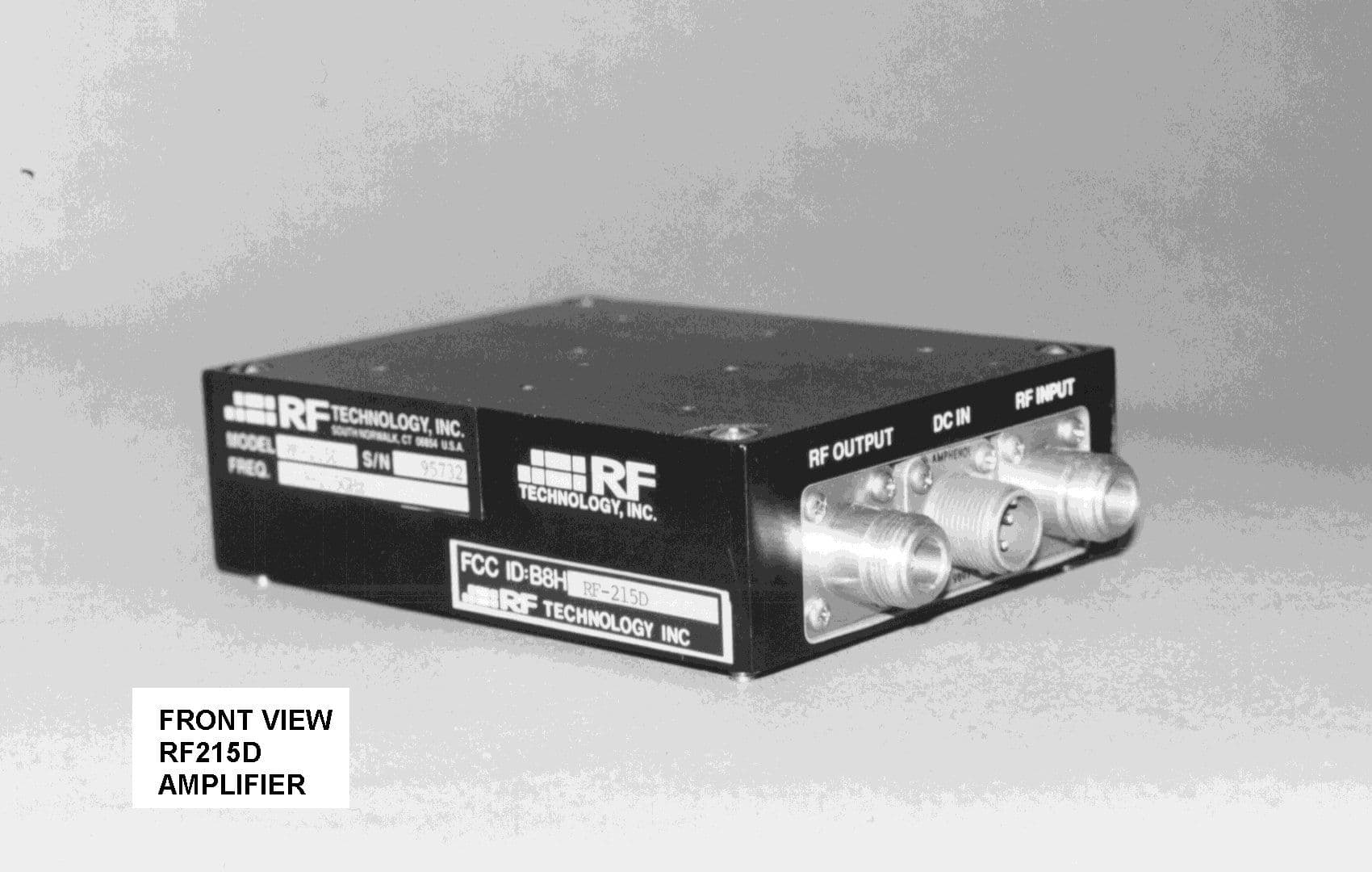
Click to zoom
Application Details
- Equipment Class
- AMP - Amplifier
- Date of Grant
- Mar 14, 2000
- Application Purpose
- Original Equipment
- Date of Application
- Oct 26, 1999
- Equipment Note
- RF Amplifier
- Frequency Range
- 1990.00000000 - 2500.00000000
- Company
- RF Technology Inc
- Country
- United States
Documents & Files
Document Text
Text extracted from the exhibit documents filed with the FCC. Open a document above to read the original.
Users Manual
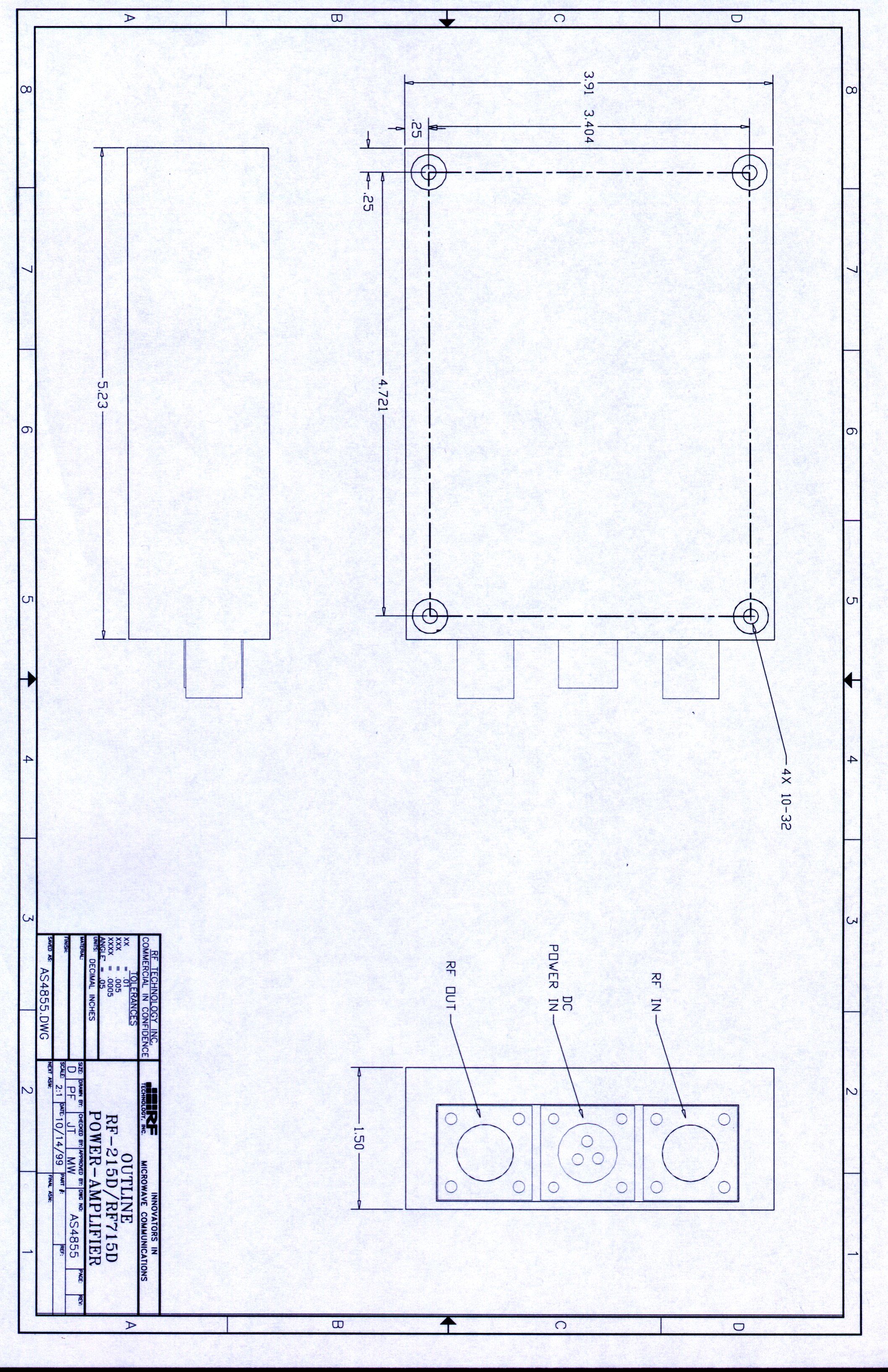
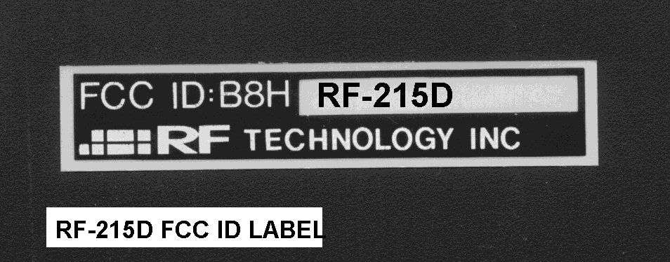
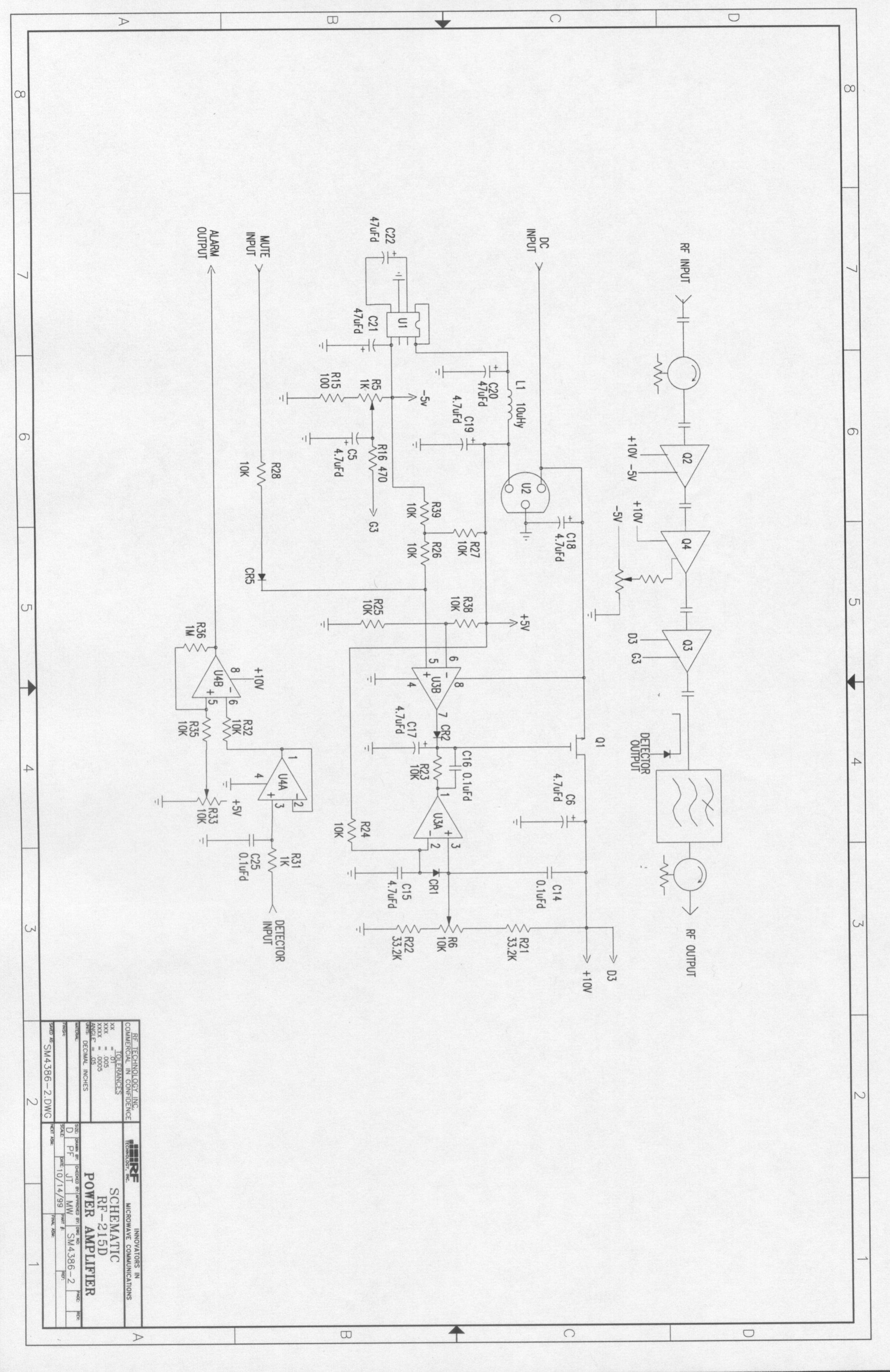
RF TECHNOLOGY, INC. 16 TESTA PLACE SOUTH NORWALK, CT 06854 PHONE 203-866-4283 FAX 203-853-3513 E-MAIL [email protected] WEB WWW.RFTECHNOLOGY.COM RF-215D AMPLIFIER MANUAL RF TECHNOLOGY, INC. RF-2185D AMPLIFIER DESCRIPTION The RF-215D amplifier consists of a regulator board and RF amplifier boards mounted in a machined aluminum weatherproof housing. The RF-215D amplifier is not field repairable due to the expertise and test equipment required to effectively make repairs. A general description of the RF amplifier section and the operation of the regulator circuit are presented for information purposes. REGULATOR: The regulator regulates the input voltage (+10.6 to +18VDC) to +10.0V and generates a –5V voltage. A +5V regulator (U2) provides the reference voltage for the regulator consisting of U3A and Q1. The regulated voltage of +10V is set by R6. The +5v output of U2 is also fed to a dc-dc converter IC (U1) through a filter consisting of L1, C19 and C20. The –5V output of U1 is used to control the current in the microwave FET transistors. A circuit (U3B) is used to turn off the regulator transistor Q1 until the –5V is present or in the event of the loss of this negative voltage. This circuit is required because a microwave FET transistor can be damaged if the +10V were to be applied before the current regulating –5V is available. The regulator circuit board also contains a detector amplifier consisting of U4A and U4B that amplifies the RF detector output to level used for indicating the presents of an RF output signal. A mute input provision is provided on the regulator board for muting the RF output when a transmitter is placed in the standby mode. RF AMPLIFIER: The RF amplifier is a three stage amplifier with input and output isolators. The input and output isolators provide an input and output impedance match and reduce the possibility of instability that could be caused by an external impedance mismatch. The circuit boards are a microwave substrate onto which is etched a computer aided designed microstrip circuit. Incorporated in the microstrip circuit design is a coupler for the RF output detector and a lowpass filter. The amplifier is operated in the saturated mode and requires an input level of 10 to 40mW (+10 to +16dBm) to achieve the rated output level of 12W (+39dBm). RF TECHNOLOGY, INC. RF-215D AMPLIFIER INSTALLATION When installing an RF-215D amplifier caution has to be taken so that the heat generated within the amplifier is removed via a good thermal connection between the amplifier and the surface it is being mounted to. The surface the amplifier is to be mounted to has be smooth and free of surface irregularities and large enough to provide a heat sink for the amplifier. Ideally this surface should be free of coatings (paint, etc.). Thermal compound has to be used between the amplifiers mounting surface and the surface it is being mounted to. An optional heat sink is available for certain applications when a mounting surface is not available that will provide an adequate heat sink for the amplifier. When installing an RF-215D outdoors the amplifier has to be mounted so that the connectors are facing down. In ENG truck applications the connectors are to be facing down during operation and to the rear of the truck then the mast is in the stowed position. Four 10-32 threaded holes are provided for mounting the amplifier refer to the RF-215D outline drawing number ASXXXX for the hole pattern. NOTE: The RF-215D amplifier can be damaged if it is operated without an adequate heat sink and/or air flow. Please consult the factory if you have any questions or concerns on installing the RF-215D amplifier. RF-215D AMPLIFIER SPECIFICATIONS Frequency Range:1990 to 2500GHz. RF Power Output:12Watts (+41dBm) RF Power Input Range:10 to 40mW (+10 to +16dBm) DC Input voltage Range:+10.6 to +18VDC DC Current:4Amps at +12VDC Operating Temperature Range:-30 to +50 Deg. C ( -22 to +122 Deg. F)
Attestation Statements
This equipment has been tested in accordance with the requirements contained in the appropriate Commission regulations. To the best of my knowledge, these tests wee performed using measurement procedures consistent with industry or Commission standards and demonstrate that the equipment complies with the appropriate standards. Each unit manufactured, imported or marketed, as defined in the Commission’s regulations, will conform to the sample tested within the variations that can be expected due to quantity production and testing on a statistical basis. I further certify that the necessary measurements wee made by RF Technology, Inc., 16 Testa Place, South Norwalk,CT, 06854. John Timm Technical Sales Manager
Test Report
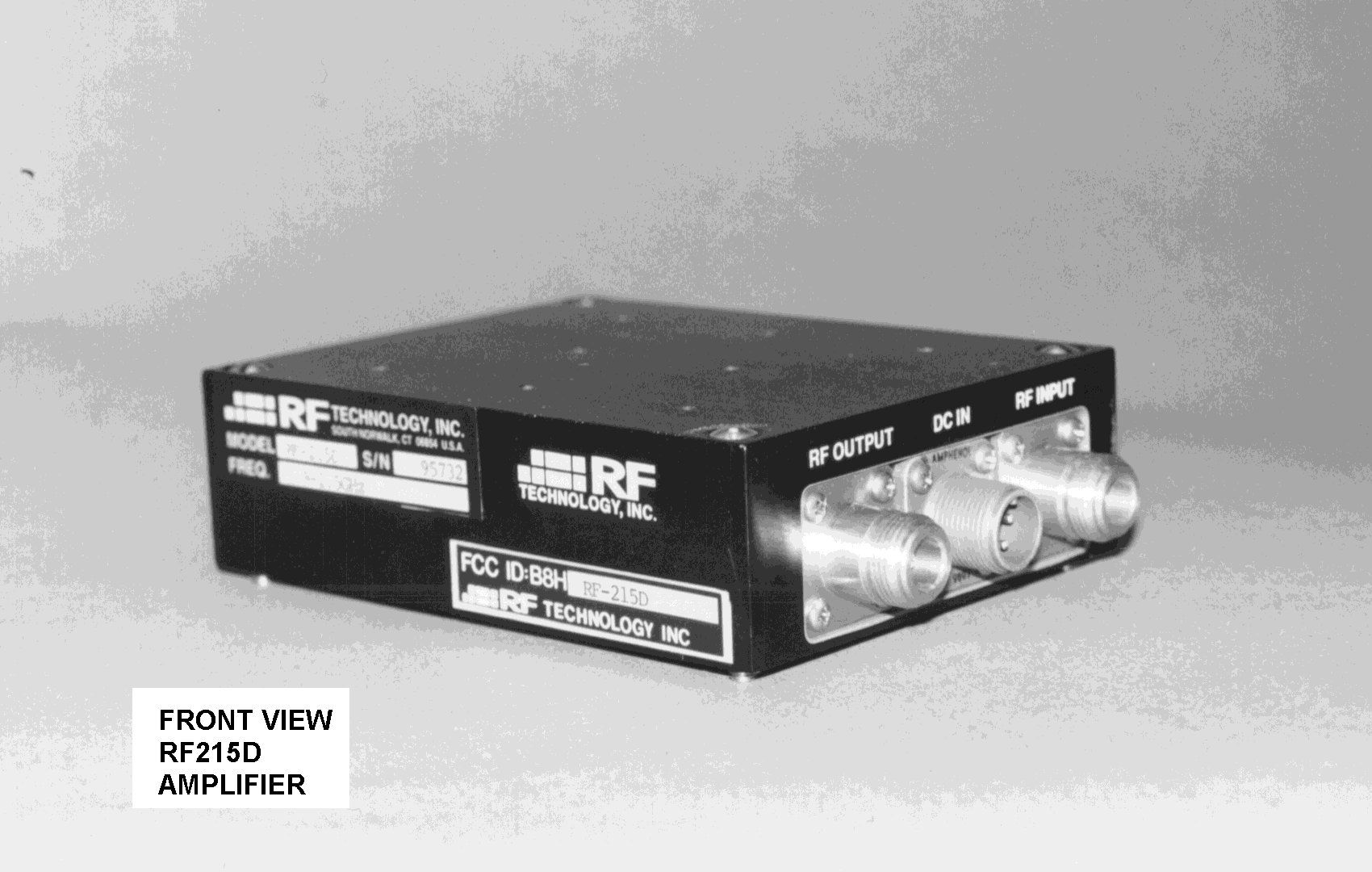
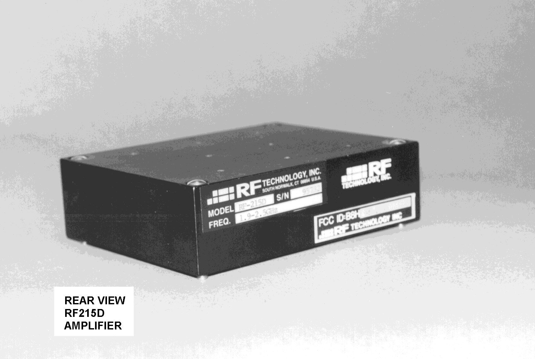
RF TECHNOLOGY, INC, 16 TESTA PLACE SOUTH NORWALK, CT 06854 PHONE 203-866-4283 FAX 203-853-3513 E-MAIL [email protected] WEB WWW.RFTECHNOLOGY.COM APPLICATION FOR CERTIFICATION OF RF-215D MICROWAVE AMPLIFIER October 27, 1999 RF TECHNOLOGY, INC. TABLE OF CONTENTS PAGE INTRODUCTION 1 TECHNICAL DESCRIPTION 1 MEASUREMENT DATA 1 Spurious Emission at antenna terminal 1 Field strength of spurious radiation 2 Occupied bandwidth 2 RF Power output 3 ENGINEERING CERTIFICATION 3 i RF TECHNOLOGY, INC. LIST OF FIGURES FIGUREDESCRIPTIONPAGE 1Spurious Emission at Antenna Test Set-up 4 2Field Strength of Spurious Radiation Test Set-up 4 3 Modulation Signal for Occupied Bandwidth Measurement 6 4 Occupied Bandwidth Spectrum 7 5 RF Output Power Set-Up 8 6Photograph of RF-215D amplifier, front view 10 includes FCC ID label 7Photograph of RF-215D amplifier, rear view 11 TABLEDESCRIPTION PAGE 1 Test equipment 9 ii RF TECHNOLOGY, INC. INTRODUCTION The RF-215D is a all solid-state amplifier, having an input power range of 10mW to 40mW with a saturated power output of 12 watts maximum, operating in the 1990 to 2500 MHz frequency band under parts 74, 78, 90, and 101 of the FCC Rules and Regulations. It is designed to be used with FM transmitters. TECHNICAL DESCRIPTION A technical description is contained in the manual. MEASUREMENT DATA In order to demonstrate compliance to the FCC Rules and Regulation, measurements were taken at RF Technology’s facilities. The results of these measurements show that the RF-215D amplifier meets or exceeds all requirements for parts 74, 78, 90 and 101. SPURIOUS EMISSION AT ANTENNA TERMINAL The antenna conducted spurious emission test set-up is shown in Figure 1. The analyzer was first tuned for a reference carrier level at the fundamental operating frequency. The output spectrum was then slowly scanned from 50MHz to 26GHz. Special attention was given to those frequencies which corresponded to possible harmonics and sub-harmonics. The FCC limit for antenna conducted spurious emission is 43+10LOG P below the main carrier. For the RF-215D with P=12W (+41dBm), this corresponds to 54dB below the main carrier, or a level of -13dBm. The second harmonic was at a level of –23dBm no other signals were noted within 20dB of the FCC limit and therefore, the amplifier meets the requirements set forth in Paragraphs 74.637, 78.103, 90.210 and 101.111. 1 RF TECHNOLOGY, INC. FIELD STRENGTH OF SPURIOUS RADIATION Case radiated spurious emission test set-up is shown in Figure 2. Observations were made at one meter from the amplifier in all planes of polarization. The output spectrum, as received at one meter, was slowly scanned upward from 50MHz to 26GHz. Special attention was given to those frequencies which corresponded to possible harmonics and sub-harmonics. A radiated reference level can be calculated using the formula: E = 30xGxP R Where: G = Power Gain of Antenna P = Amplifier Power in Watts R = Distance from radiator at which field intensity is measured. In this case: G = 1.64 (gain of dipole over isotropic) P = 12 Watts R = 1 meter Therefore: E = 30x1.64x12 = 24.298 V/meter = 147.7dBuV/M 1 The FCC requires case radiated signals to be attenuated by a factor of 43+10LOG P or 43+10log 12 = 53.8dB. Thus, 147.7dBuv/M reduced by 53.8dB = 93.9dBuv/M. No case radiated signals were detected within 20dB of the FCC limit and therefore the amplifier meets the requirements set forth in Paragraphs 74.637, 78.103, 90.210 and 101.111 OCCUPIED BANDWIDTH To measure the occupied bandwidth, the equipment was set up as shown in Figure 1, and the transmitter was modulated by a multiburst video signal and the audio subcarrier was modulated by a 1KHz sinewave, which produced a modulated output that was then fed to the RF-215D amplifier. The output of the RF_218D amplifier was viewed on a spectrum analyzer. Since the spectrum is symmetrical, about Fo, calculations were performed on one-half of the spectrum and then doubled to find the occupied bandwidth. A reference level was set at Fo and the amplitude readings were taken every 0.5MHz from Fo to Fo+12MHz. The readings were then converted to a linear scale and the total power was then calculated using Simpson’s Rules of Numerical Integration. 2 RF TECHNOLOGY, INC. The total power was then multiplied by 99.5% to obtain the 0.5% power point. Calculations were then performed to find the frequency that corresponds to the 0.5% power point. From these calculations the occupied bandwidth was determined to be 15.2MHz. RF POWER OUTPUT The RF power output test set up is shown in Figure 3. The input power to the RF-215D amplifier was varied across its input range from 10mW to 40mW with no change in its output power of 12 watts. The DC input voltage was varied across the range of 10.6 to 18V with no change in output power. . ENGINEERING CERTIFICATION It is hereby certified that the Certification Tests on RF Technology’s RF-215D Microwave Amplifier were made under my supervision and that all the data submitted in the attached report is true and correct to the beast of my knowledge and belief. -------------------------------- John Timm Technical Sales Manager QUALIFICATIONS Mr. Timm has been employed by RF Technology Inc. for over 20 years. He received an A.A.S. degree from Norwalk State Technical College in 1971. He has been in the Engineering Department and has worked on the development and testing of equipment that has been submitted to the FCC for approval. PRODUCTION RF Technology, Inc. is planning a quantity production of the RF-215D Microwave amplifier. 3 RF TECHNOLOGY, INC. 0.05 to 26GHz FIGURE 1 – SPURIOUS EMISSION AT ANTENNA TEST SET-UP FIGURE 2 – FIELD STRENGTH OF SPURIOUS RADIATION TEST SET-UP 4 RF-202D TRANSMITTER RF-215D AMPLIFIER 40dB PAD HP8592 SPECTRUM ANALYZER RF-202D TRANSMITTER RF-215D AMPLIFIER 50 OHM LOAD 1 Meter HP8592 SPECTRUM ANALYZER RF TECHNOLOGY, INC. FIGURE 3 – OUTPUT POWER VERSUS DC VOLTAGE AND RF INPUT POWER TEST SET-UP 5 RF-202D TRANSMITTER VARIABLE …
Text truncated - open the document above for the full version.
Test Setup Photos
RF TECHNOLOGY, INC. 0.05 to 26GHz FIGURE 1 – SPURIOUS EMISSION AT ANTENNA TEST SET-UP FIGURE 2 – FIELD STRENGTH OF SPURIOUS RADIATION TEST SET-UP 4 RF-202D TRANSMITTER RF-215D AMPLIFIER 40dB PAD HP8592 SPECTRUM ANALYZER RF-202D TRANSMITTER RF-215D AMPLIFIER 50 OHM LOAD 1 Meter HP8592 SPECTRUM ANALYZER RF TECHNOLOGY, INC. FIGURE 3 – OUTPUT POWER VERSUS DC VOLTAGE AND RF INPUT POWER TEST SET-UP RF-202D TRANSMITTER VARIABLE ATTENUATOR RF-215D AMPLIFIER 30dB PAD POWER METER DC POWER SUPPLY
Contact Information
Applicant
John Timm(Technical Sales Manager)
203 866-4283Fax: 203 853-3513
Technical Specifications
| # | Rule Parts | Frequency Range | Power Output | Emission | Tolerance |
|---|---|---|---|---|---|
| 1 | 74,78,90,101 | 1.99 GHz - 2.50 GHz | 12 W | F8W | Amp |
Other Applications from RF Technology Inc

B8HUCL-130T
Feb 02, 2000TNB - Licensed Non-Broadcast Station Transmitter
Equipment Class
TNB - Licensed Non-Broadcast Station Transmitter
B8HRF-715D
Feb 22, 1999AMP - Amplifier
Equipment Class
AMP - AmplifierB8HUCL-20T
Mar 19, 1997TBC - Licensed Broadcast Station Transmitter
Equipment Class
TBC - Licensed Broadcast Station TransmitterB8HUCL-70T
Feb 05, 1997TNB - Licensed Non-Broadcast Station Transmitter
Equipment Class
TNB - Licensed Non-Broadcast Station TransmitterB8HUPL-13000
May 05, 1996TNB - Licensed Non-Broadcast Station Transmitter
Equipment Class
TNB - Licensed Non-Broadcast Station Transmitter