B94500Lap Top with Spread Spectrum Transmitter
HP Inc.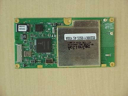
Click to zoom
Application Details
- Equipment Class
- DSS - Part 15 Spread Spectrum Transmitter
- Date of Grant
- Jun 07, 2001
- Application Purpose
- Original Equipment
- Date of Application
- Jun 07, 2001
- Equipment Note
- Lap Top with Spread Spectrum Transmitter
- Frequency Range
- 2400.00000000 - 2483.50000000
- Company
- HP Inc.
- Country
- United States
Documents & Files
Document Text
Text extracted from the exhibit documents filed with the FCC. Open a document above to read the original.
Users Manual
HP Notebook PC Startup Guide 2 Startup Guide Notice This manual and any examples contained herein are provided “as is” and are subject to change without notice. Hewlett-Packard Company makes no warranty of any kind with regard to this manual, including, but not limited to, the implied warranties of merchantability and fitness for a particular purpose. Hewlett-Packard Co. shall not be liable for any errors or for incidental or consequential damages in connection with the furnishing, performance, or use of this manual or the examples herein. Consumer transactions in Australia and the United Kingdom: The above disclaimers and limitations shall not apply to Consumer transactions in Australia and the United Kingdom and shall not affect the statutory rights of Consumers. © Copyright Hewlett-Packard Company 2000-2001. All rights reserved. Reproduction, adaptation, or translation of this manual is prohibited without prior written permission of Hewlett-Packard Company, except as allowed under the copyright laws. The programs that control this product are copyrighted and all rights are reserved. Reproduction, adaptation, or translation of those programs without prior written permission of Hewlett-Packard Co. is also prohibited. Portions of the programs that control this product may also be copyrighted by Microsoft Corporation, SystemSoft Corp., Phoenix Technologies, Ltd., ATI Technologies Inc., and Adobe Systems Incorporated. See the individual programs for additional copyright notices. This product incorporates copyright protection technology that is protected by method claims of certain U.S. patents and other intellectual property rights owned by Macrovision Corporation and other rights owners. Use of this copyright protection technology must be authorized by Macrovision Corporation and is intended for home and other limited viewing uses only unless otherwise authorized by Macrovision Corporation. Reverse engineering or disassembly is prohibited. Microsoft®, MS-DOS®, and Windows® are U.S. registered trademarks of Microsoft Corporation. Pentium® and the Intel Inside logo are U.S. registered trademarks and Celeron™ and SpeedStep™ are U.S. trademarks of Intel Corporation. TrackPoint™ is a U.S. trademark of International Business Machines. Adobe® and Acrobat® are trademarks of Adobe Systems Incorporated. Hewlett-Packard Company HP Notebook Customer Care 1000 NE Circle Blvd., MS 425E Corvallis, OR 97330 Startup Guide 3 Important Safety Information CAUTION To reduce the risk of fire, use only No. 26 AWG or larger telecommunications line cord to connect a modem to the telephone wall jack. When using your computer with a telephone connection, always follow basic safety precautions to reduce the risk of fire, electric shock, and injury to persons: • Do not use this product with a telephone connection near water (for example, near a bathtub, sink, swimming pool, or in a wet basement). • Avoid using a telephone connection (other than a cordless type) during an electrical storm. There may be a remote risk of electric shock from lighting. • Do not use a telephone connection to report a gas leak in the vicinity of the leak. • Use only the power cord and batteries indicated in this manual. Do not dispose of batteries in a fire. They may explode. Check with local codes for possible special disposal instructions. HP Software Product License Agreement Your HP product contains software programs. CAREFULLY READ THIS LICENSE AGREEMENT BEFORE PROCEEDING TO OPERATE THIS EQUIPMENT. RIGHTS IN THE SOFTWARE ARE OFFEREDONLY ON THE CONDITION THAT THE CUSTOMER AGREES TO ALL TERMS AND CONDITIONS OF THE LICENSE AGREEMENT. PROCEEDING TO OPERATE THE EQUIPMENT INDICATES YOUR ACCEPTANCE OF THESE TERMS AND CONDITIONS. IF YOU DO NOT AGREE WITH THE TERMS OF THE LICENSE AGREEMENT, YOU MUST NOW EITHER REMOVE THE SOFTWARE FROM YOUR HARD DISK DRIVE AND DESTROY THE MASTER DISKETTES, OR RETURN THE COMPLETE HP PRODUCT AND SOFTWARE FOR A FULL REFUND. PROCEEDING WITH CONFIGURATION SIGNIFIES YOUR ACCEPTANCE OF THE LICENSE TERMS. UNLESS OTHERWISE STATED BELOW, THIS HP SOFTWARE LICENSE AGREEMENT SHALL GOVERN THE USE OF ALL SOFTWARE THAT IS PROVIDED TO YOU AS PART OF THE HP PRODUCT AND SHALL SUPERSEDE ANY OTHER SOFTWARE WARRANTY STATEMENT THAT MAY BE INCLUDED IN THIS HP PRODUCT OR MAY BE FOUND ONLINE. 4 Startup Guide Operating system and software applications by Microsoft are licensed to you under the Microsoft License Agreement contained in the Microsoft documentation or displayed on your screen when Microsoft Software Products are launched. Other non-HP Software and Operating Systems are covered by the appropriate vendor license. The following License Terms govern the use of the HP software: USE. Customer may use the software on any one HP product. Customer may not network the software or otherwise use it on more than one HP product. Customer may not reverse assemble or decompile the software unless authorized by law. COPIES AND ADAPTATIONS. Customer may make copies or adaptations of the software a) for archival purposes or (b) when copying or adaptation is an essential step in the use of the software with an HP product so long as the copies and adaptations are used in no other manner. OWNERSHIP. Customer agrees that he/she does not have any title or ownership of the software, other than ownership of the physical media. Customer acknowledges and agrees that the software is copyrighted and protected under the copyright laws. Customer acknowledges and agrees that the software may have been developed by a third party software supplier named in the copyright notices included with the software, who shall be authorized to hold the Customer responsible for any copyright infringement or violation of this Agreement. PRODUCT RECOVERY CD-ROM. If your HP product was shipped with a product recovery CD-ROM: (i) The product recovery CD-ROM and/or support utility software may only be used for restoring the hard disk of the HP product with which the product rec…
Text truncated - open the document above for the full version.
Block Diagram
BLOCK DIAGRAM
Cover Letter(s)
Federal Communication Commission Equipment Authorization Division, Application Processing Branch 7435 Oakland Mills Road Columbia, MD 21048 October 16, 2000 TO WHOM IT MAY CONCERN Pursuant to Paragraphs §0.457 and 0.459 of the Commission’s Rules (47 C.F.R.) and Section §552(b)(4) of the Freedom of Information Act, Hewlett Packard Company requests confidentiality for the following products: FCC ID Number Product Title/Model B94500 HP OmniBook 500 series is also the HP pavilion z1xxx series (where x= any digit from 0-9) For the product stated above, we request that the following information be held confidential: 1) Electrical Schematics of the Circuitry 2) BOM 3) Gerber files except USBger_4 No other items submitted as part of the equipment authorization filing process are deemed confidential. The above exhibits contain Hewlett Packard Company trade secrets and proprietary information that could be of benefit to our competitors regarding the design of our mobile handset. This material is not customarily available to the general public and we request that it be withheld from public inspection. If you have any questions, please feel free to contact me at the address shown below. Sincerely, Lothar Schmidt Technical Manager
ID Label/Location Info
D D 1 2 3 4 5 6 7 ABCE 7 6 5 4 3 2 1 ECBA LTR NAME MODEL MATERIAL FINISH DATE SCALE UNIT MM DWG. NO. APPROVED DESIGNED DRAWN REV 3A 3A 3C TOL. + - 1 PLC2 PLCANGLE 7F, 116 HOU KANG ST. SHIN LIN, TAIPEI, TAIWAN, R.O.C. ITEMDESCRIPTION REVISIONS DESCRIPTION DATEAPP THE 3RD PROJECTION PART NO. Quanta Computer Inc. 2 1 3 FIRST RELEASE Rita S/N HCJT1016 1/1 HCJT1016 90.06.01 90.06.01 J T1 WIRELESS LABEL 3B Rita 0.1 0682 3 8 . 5 64.0 This device incorporates TX FCC ID : B94500 DT#, 0.
ID Label/Location Info
COMPLIES WITH CANADIAN EMC CLASS B REQUIREMENTS. Conforme à la classe B des normes Canadiennes de compatibilité électromagnétiques <<CEM>>. 3.16A (3,16A) INPUT: + - Rev.A 19V Apparatus Claims of U.S. Patent Nos. 4,631,603, 4,577,216, 4,819,098, and 4,907,093 licensed for limited viewing uses only. SEE MANUAL FOR BATTERY AND AC ADAPTER INFORMATION. hp omnibook 500 CM Rev.A COMPLIES WITH CANADIAN EMC CLASS B REQUIREMENTS. Conforme à la classe B des normes Canadiennes de compatibilité électromagnétiques <<CEM>>. 3.16A (3,16A) INPUT: + - Rev.A 19V Apparatus Claims of U.S. Patent Nos. 4,631,603, 4,577,216, 4,819,098, and 4,907,093 licensed for limited viewing uses only. SEE MANUAL FOR BATTERY AND AC ADAPTER INFORMATION. hp omnibook 500 CM Rev.A Bar-Code Label, Stepped Recess24.0 x 57mm Stepped Recess Bar-Code Label, Stepped Recess24.0 x 57mm Stepped Recess #2 Microsoft COA Label NEW = 28mm X 70mm (on-demand COA label available in September 2001) ALTERNATIVE LOCATION: (1) On Demand COA Label; fits as shown, but very tight. NOT Recommended! #1 Microsoft COA Label NEW = 28mm X 70mm (on-demand COA label available in September 2001) PROPOSED LOCATION: (1) On Demand COA Label; fits as shown #2 Microsoft COA Label NEW = 28mm X 70mm (on-demand COA label available in September 2001) ALTERNATIVE LOCATION: (1) On Demand COA Label; fits as shown, but very tight. NOT Recommended! #1 Microsoft COA Label NEW = 28mm X 70mm (on-demand COA label available in September 2001) PROPOSED LOCATION: (1) On Demand COA Label; fits as shown View 6: Bottom Case, JAWs 1.0 & 1.5 non-wireless Regulatory Label (generic content) HP Regulatory Symbol Label & HP Prime Label location Telecom Label = 60.0 x 62.0mm (reces = + 0.3mm tolerance each side) JAWS COA Label Fit (dwg #2 of 2) 05.14.01 _________________________________ NEW COA LABEL SIZE (available September 2001, per Microsoft) (1) Print on-demand COA label = 28mm X 70mm hp restricted Regulatory Symbol Label Telecom Symbol/Sticker Label Taiwan Recycle Label (12mm X 15mm) View 6: Bottom Case, JAWs 1.5 wireless Regulatory Label (generic content) HP Regulatory Symbol Label & HP Prime Label location Telecom Label = 60.0 x 62.0mm (reces = + 0.3mm tolerance each side) WIRELESS Regulatory Symbol Label 64.0mm WIDE x 38.5mm TALL (NO recess; label to a be applied to the surface of the product RAM door in this location) THIS SPACE MUST BE RESERVED FOR THE APPLICATION OF A WIRELESS MARKING REGULATORY LABEL. Regulatory Symbol Label Telecom Symbol/Sticker Label Taiwan Recycle Label (12mm X 15mm) Wireless Symbol Label (64.0mm X 38.5mm) Bar-Code Label
ID Label/Location Info
Statement regarding the labeling requirements The wire less approval label will include the following statement: This device complies with Part 15 of the FCC Rules. Operation is subject to the following two conditions: (1) this device may not cause harmful interference, and (2) this device must accept any interference received, including interference that may cause undesired operation.
Operational Description
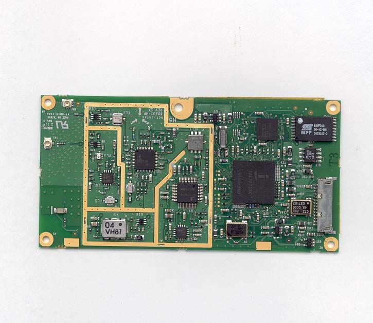
Basic Operation Principle of 802MIP Actiontec Electronics, Inc. 4/2001 The Wireless LAN portion of 802MIP combo card is a 2.4GHz ISM Band DSSS Radio. It is designed to operate using IEEE 802.11b WLAN Standard for use in wireless networking systems. The Radio consists of 4 major ICs, which are ISL3685, HFA3783, ISL3984, ISL3874, and few support ICs. It operates at maximum transmit rate 11Mb/s, back off rates 5.5, 2 and 1 Mb/s. The modulation schemes include CCK (Complementary Code Keying), DQPSK and DBPSK depending on what transmit bit rate it operates at. The radio card interfaces to PC through a MiniPCI bus. Transmitter path The Ethernet data comes through the MiniPCI interface, the Host I/O interface to the MAC section of ISL3874. The signal then flows into the data router where it is converted from Ethernet to 802.11b protocol. After the signal is converted, a radio preamble and header is added to it and passed to the I/O of BBP (Base Band Processor) section of ISL3874 via PHY I/O, RADIO I/O. There is also support circuitry, such as outboard SRAM and flash ROM, which contains the firmware controlling the radio. In TX modulator of BBP section, differential phase shift keying modulation schemes DBPSK, DQPSK and CCK, with data scrambling capability, are fulfilled to provide a variety of data rates--DBPSK for 1 Mb/s, DQPSK for 2 Mb/s and CCK for 5.5 and 11Mb/s. The signal, which now is two separate quadrature components I and Q, then flows to the quad IF chip HFA3783 through D/A converters. At TX side of BBP, there is also TX ALC (Automatic Level Control) circuitry, which is part of the TX ALC loop. The loop keeps TX output power to be consistent so that prevent the power spectrum from regrowth. HFA3783 is now the dual up conversion mixers (dual down conversion mixers for RX). The signal upconverts to an IF frequency of 374 MHz and passes into a variable gain amplifier, which is also a part of the ALC loop. Next, it passes through the switched TX/RX shared SAW filter into ISL3685 and then upconverts again to a RF frequency from 2.412~2.484 GHz, depending on the channel selection. The signal flows through a pre-amplifier, two band pass filters, which block all the unwanted emissions such as image components, harmonics and spurious stuff, into ISL3984 power amplifier. The output of the power amplifier is then fed through another band pass filter that is about 85 MHz bandwidth to one of the antennas. Receiver path The receive signal traveling through the air is received by the dual diversity antennas. The circuits will switch to the antenna which provides better RSSI (Received Signal Strength Indication). The RF signal then feeds into an 85 MHz band pass filter, which blocks all the unwanted components such as image frequency. The signal again is amplified using the LNA within ISL3685 and mixed down to the IF frequency of 374 MHz. The PLL and synthesizer select the channel frequency using Low Side Injection. The mixer outputs are then fed through the IF SAW filter that provides image rejection into HFA3783, which is now a quad down converter. HFA3783 also provides RSSI to BBP of ISL3874. There is a two stage analog AGC (Automatic Gain Control) circuit which adjusts the gain to compensate the signal strength differences. The output of the twin AGC’s provides a constant level signal to the I and Q down converters, which convert the IF to both I and Q signals to BBP. A second frequency synthesizer, which uses ISL3183 as its VCO, feeds the I and Q mixers with a same frequency signal that is phase shifted by 90°. The I and Q signals that are fed into BBP of ISL3874 are converted into digital signals via a dual A/D converters then flow through the digital AGC control circuit followed by the digital demodulator. The correlation codes that BBP generates properly detect the transmitted complimentary codes. In here the automatic antenna selection is also done by taking RSSI as the reference. The output of the digital demodulator is sent into an I/O interface of MAC section. The digital codes then flow into the PHY I/O interface and into the MAC protocol engine. The MAC of ISL3874 converts the signal protocol from 802.11b to Ethernet and finally passes that data through the HOST I/O interface to the PC.
Test Report
CETECOM Inc. CETECOM Inc. 411 Dixon Landing Road, Milpitas, CA-95035, USA Phone: +1 408 586 6200 Fax: +1 408 586 6299 www.cetecomusa.com Issued test report consists of 52 Pages Page 1 (52) Test report no.: 141FCC/2001 FCC Part 15.247 HP OmniBook 500 RECOGNIZED BY INDUSTRY CANADA IC - 3925 CETECOM Inc. Test report no.:141FCC/2001 Issued date:2001-05-10 Page 2 (52) Table of Contents 1 General information 1.1 Notes 1.2 Testing laboratory 1.3 Details of applicant 1.4 Application details 1.5 Test item 1.6 Test standards 2 Technical test 2.1 Summary of test results 2.2 Test report 1 General information 1.1 Notes The test results of this test report relate exclusively to the test item specified in 1.5. The CETECOM Inc. USA does not assume responsibility for any conclusions and generalisations drawn from the test results with regard to other specimens or samples of the type of the equipment represented by the test item. The test report may only be reproduced or published in full. Reproduction or publication of extracts from the report requires the prior written approval of the CETECOM Inc. USA. CETECOM Inc. Test report no.:141FCC/2001 Issued date:2001-05-10 Page 3 (52) 1.2 Testing laboratory CETECOM Inc. 411 Dixon Landing Road, Milpitas, CA-95035, USA Phone: +1 408 586 6200 Fax: +1 408 586 6299 E-mail: [email protected] Internet: www.cetecomusa.com 1.3 Details of applicant Name : Hewlett Packard Co.; Mobile Computing Division Street : 1000 NE Circle Blvd. City : Corvallis, OR 97330 Country : USA Telephone : +1 541 715 2171 Telefax : +1 541 715 3607 Contact : Kathy Warnock e-mail : [email protected] 1.4 Application details Date of receipt of application : 2001-04-01 Date of receipt of test item : 2001-04-15 Date of test : 2001-04-18/19/20 1.5 Test item Manufacturer : Hewlett Packard. Address : See above Model number : HP OmniBook 500 Series Type Designation : Additional informations: HP OmniBook 500 Series Frequency : 2.412 – 2.484 GHz Type of modulation : DBPSK at 1Mb/s; DQPSK at 2Mb/s; CCK at 5.5.and 11Mb/s Number of channels : 11 Channels in US Antenna : Integral Power supply : 5.0V Type of equipment : Temperature range : 0°C - +35°C Tests were carried out at the maximum number of channels available (13) in the test software. The US version will set to 11 channels only. 1.6 Test standards FCC Part 15 §15.247 The tests were done following the public notice DA 00-705 released March 30, 2000 CETECOM Inc. Test report no.:141FCC/2001 Issued date:2001-05-10 Page 4 (52) 2 Technical test 2.1 Summary of test results No deviations from the technical specification(s) were ascertained in the course of the tests performed. Technical responsibility for area of testing : 2001-05-10 EMC& Radio Lothar Schmidt Date Section Name Signature CETECOM Inc. Test report no.:141FCC/2001 Issued date:2001-05-10 Page 5 (52) 2.2 Testreport TEST REPORT Testreport no. : 141FCC/2001 HP OmniBook 500 CETECOM Inc. Test report no.:141FCC/2001 Issued date:2001-05-10 Page 6 (52) TEST REPORT REFERENCE LIST OF MEASUREMENTS Paragraph PARAMETER TO BE MEASURED PAGE Transmitter parameters § 15.247 (a)(2) Spectrum Bandwith of a DSSS System 7 § 15.247 (b)(1) Maximum peak output power 11 § 15.247 (c)(1) Emission limitations 16 § 15.247 (d) Power Spectral Density 33 § 15.247 (e) Processing Gain of DSSS System 37 Receiver parameters § 15.209 Spurious radiations - Radiated 39 Test equipment listing 47 Test Site 48 Photographs of the equipment 50 NOTE: Conducted Emissions as per § 15.107 are not applicable for the EUT since it is a built in a laptop computer. The Laptop was measured in accordance with FCC part 15 B including the Wireless LAN . CETECOM Inc. Test report no.:141FCC/2001 Issued date:2001-05-10 Page 7 (52) SPECTRUM BANDWITH OF DSSS-SYSTEM SUBCLAUSE § 15.247 (a)(2) TEST CONDITIONS 6 dB BANDWIDTH ( kHz ) Frequency (MHz) 2412 2442 2472 T nom ( 20 )° °° °C V nom ()V 10020 11422 10020 Measurement uncertainty ±3dB LIMIT SUBCLAUSE §15.247(a) (2) The minimum 6dB bandwith shall shall be at least 500 KHz CETECOM Inc. Test report no.:141FCC/2001 Issued date:2001-05-10 Page 8 (52) SPECTRUM BANDWITH OF DSSS-SYSTEM SUBCLAUSE § 15.247 (a)(2) 2412 MHz LIMIT SUBCLAUSE §15.247(a) (2) The minimum 6dB bandwith shall shall be at least 500 KHz , here 10.02 MHz ANALYZER SETTINGS: RBW=100KHz , VBW=1MHz CETECOM Inc. Test report no.:141FCC/2001 Issued date:2001-05-10 Page 9 (52) SPECTRUM BANDWITH OF DSSS-SYSTEM SUBCLAUSE § 15.247 (a)(2) 2442 MHz LIMIT SUBCLAUSE §15.247(a) (2) The minimum 6dB bandwith shall shall be at least 500 KHz , here 11.42 MHz ANALYZER SETTINGS: RBW=100KHz , VBW=1MHz CETECOM Inc. Test report no.:141FCC/2001 Issued date:2001-05-10 Page 10 (52) SPECTRUM BANDWITH OF DSSS-SYSTEM SUBCLAUSE § 15.247 (a)(2) 2472 MHz LIMIT SUBCLAUSE §15.247(a) (2) The minimum 6dB bandwith shall shall be at least 500 KHz , here 10.02 MHz ANALYZER SETTINGS: RBW=100KHz , VBW=1MHz 2.472GHz CETECOM Inc. Test report no.:141FCC/2001 Issued date:2001-05-10 Page 11 (52) MAXIMUM PEAK OUTPUT POWER SUBCLAUSE § 15.247 (b) (1) (CONDUCTED) TEST CONDITIONS MAXIMUM PEAK OUTPUT POWER (dBm) Frequency (MHz) 2412 2442 2472 Pk 16.81 Pk 17.06 Pk 17.22 T nom ( 23 )° °° °C V nom ()V Av 11.80 Av 12.05 Av 11.84 Pk 17.47 Pk 17.60 Pk 17.57 T nom ( 0 )° °° °C V nom ()V Av 12.39 Av 12.70 Av 12.45 Pk 16.27 Pk 16.49 Pk 16.13 T nom ( 35 )° °° °C V nom ()V Av 11.17 Av 11.45 Av 10.96 Measurement uncertainty ±3dB LIMIT SUBCLAUSE § 15.247 (b) (1) Frequency range RF power output 2400-2483.5 MHz / 5725 – 5850 MHz 1.0 Watt CETECOM Inc. Test report no.:141FCC/2001 Issued date:2001-05-10 Page 12 (52) MAXIMUM PEAK OUTPUT POWER (EIRP) SUBCLAUSE § 15.247 (b) (1) (RADIATED) TEST CONDITIONS MAXIMUM PEAK OUTPUT POWER (dBm) Frequency (MHz) 2412 2442 2472 Pk17.67 Pk18.43 Pk 18.85 T nom ( 23 )° °° °C V nom ()V Av12.57 Av13.23 Av 13.75 Maximum deviation from output power under extreme test conditions (dBc) not performed not performed not performed Measurement uncertainty ±3dB LIMIT SUBCLAUSE § 15.24…
Text truncated - open the document above for the full version.
Test Report
Processing Gain ISL37400M 11Mbps CHANNEL 6 Processing Gain Gp = (S/N)o + Mj + Lsys Freq.Gp(S/N)oMj=J/SLsysJammerPER (MHz)(dB)(dB)(dB)(dB)(dBm)(%) 2428.5023.916.45.52.0-57.2<=8.0 2428.5523.916.45.52.0-57.2<=8.0 2428.6023.916.45.52.0-57.2<=8.0 2428.6523.816.45.42.0-57.3<=8.0 2428.7023.816.45.42.0-57.3<=8.0 2428.7524.016.45.62.0-57.1<=8.0 2428.8024.116.45.72.0-57.0<=8.0 2428.8524.116.45.72.0-57.0<=8.0 2428.9024.216.45.82.0-56.9<=8.0 2428.9524.116.45.72.0-57.0<=8.0 2429.0024.416.46.02.0-56.7<=8.0 2429.0524.316.45.92.0-56.8<=8.0 2429.1024.316.45.92.0-56.8<=8.0 2429.1524.316.45.92.0-56.8<=8.0 2429.2024.416.46.02.0-56.7<=8.0 2429.2523.716.45.32.0-57.4<=8.0 2429.3023.316.44.92.0-57.8<=8.0 2429.3523.216.44.82.0-57.9<=8.0 2429.4022.216.43.82.0-58.9<=8.0 2429.4521.316.42.92.0-59.8<=8.0 2429.5021.216.42.82.0-59.9<=8.0 2429.5521.116.42.72.0-60.0<=8.0 2429.6021.116.42.72.0-60.0<=8.0 2429.6521.016.42.62.0-60.1<=8.0 2429.7021.016.42.62.0-60.1<=8.0 2429.7520.816.42.42.0-60.3<=8.0 2429.8020.716.42.32.0-60.4<=8.0 2429.8521.116.42.72.0-60.0<=8.0 2429.9021.016.42.62.0-60.1<=8.0 2429.9521.116.42.72.0-60.0<=8.0 2430.0020.916.42.52.0-60.2<=8.0 2430.0520.916.42.52.0-60.2<=8.0 2430.1020.516.42.12.0-60.6<=8.0 2430.1519.516.41.12.0-61.6<=8.0 2430.2019.516.41.12.0-61.6<=8.0 2430.2519.016.40.62.0-62.1<=8.0 2430.3019.016.40.62.0-62.1<=8.0 2430.3518.716.40.32.0-62.4<=8.0 2430.4018.716.40.32.0-62.4<=8.0 2430.4518.516.40.12.0-62.6<=8.0 2430.5018.416.40.02.0-62.7<=8.0 2430.5518.416.40.02.0-62.7<=8.0 2430.6018.416.40.02.0-62.7<=8.0 2430.6518.116.4-0.32.0-63.0<=8.0 2430.7017.916.4-0.52.0-63.2<=8.0 2430.7517.416.4-1.02.0-63.7<=8.0 2430.8017.416.4-1.02.0-63.7<=8.0 2430.8517.116.4-1.32.0-64.0<=8.0 Prepared by: D. KalcikPage 15/23/01 Processing Gain ISL37400M 11Mbps CHANNEL 6 Processing Gain Gp = (S/N)o + Mj + Lsys Freq.Gp(S/N)oMj=J/SLsysJammerPER (MHz)(dB)(dB)(dB)(dB)(dBm)(%) 2430.9017.116.4-1.32.0-64.0<=8.0 2430.9516.916.4-1.52.0-64.2<=8.0 2431.0016.816.4-1.62.0-64.3<=8.0 2431.0516.716.4-1.72.0-64.4<=8.0 2431.1016.716.4-1.72.0-64.4<=8.0 2431.1516.316.4-2.12.0-64.8<=8.0 2431.2016.516.4-1.92.0-64.6<=8.0 2431.2516.416.4-2.02.0-64.7<=8.0 2431.3016.316.4-2.12.0-64.8<=8.0 2431.3516.316.4-2.12.0-64.8<=8.0 2431.4015.816.4-2.62.0-65.3<=8.0 2431.4515.916.4-2.52.0-65.2<=8.0 2431.5015.716.4-2.72.0-65.4<=8.0 2431.5515.516.4-2.92.0-65.6<=8.0 2431.6015.416.4-3.02.0-65.7<=8.0 2431.6515.216.4-3.22.0-65.9<=8.0 2431.7015.116.4-3.32.0-66.0<=8.0 2431.7515.016.4-3.42.0-66.1<=8.0 2431.8015.016.4-3.42.0-66.1<=8.0 2431.8514.916.4-3.52.0-66.2<=8.0 2431.9015.016.4-3.42.0-66.1<=8.0 2431.9515.116.4-3.32.0-66.0<=8.0 2432.0015.116.4-3.32.0-66.0<=8.0 2432.0515.116.4-3.32.0-66.0<=8.0 2432.1015.016.4-3.42.0-66.1<=8.0 2432.1514.816.4-3.62.0-66.3<=8.0 2432.2014.916.4-3.52.0-66.2<=8.0 2432.2514.916.4-3.52.0-66.2<=8.0 2432.3014.816.4-3.62.0-66.3<=8.0 2432.3514.616.4-3.82.0-66.5<=8.0 2432.4014.316.4-4.12.0-66.8<=8.0 2432.4514.516.4-3.92.0-66.6<=8.0 2432.5014.616.4-3.82.0-66.5<=8.0 2432.5514.516.4-3.92.0-66.6<=8.0 2432.6014.316.4-4.12.0-66.8<=8.0 2432.6514.316.4-4.12.0-66.8<=8.0 2432.7014.216.4-4.22.0-66.9<=8.0 2432.7514.116.4-4.32.0-67.0<=8.0 2432.8014.116.4-4.32.0-67.0<=8.0 2432.8513.816.4-4.62.0-67.3<=8.0 2432.9013.516.4-4.92.0-67.6<=8.0 2432.9513.716.4-4.72.0-67.4<=8.0 2433.0013.616.4-4.82.0-67.5<=8.0 2433.0513.516.4-4.92.0-67.6<=8.0 2433.1013.516.4-4.92.0-67.6<=8.0 2433.1513.516.4-4.92.0-67.6<=8.0 2433.2013.616.4-4.82.0-67.5<=8.0 2433.2513.716.4-4.72.0-67.4<=8.0 Prepared by: D. KalcikPage 25/23/01 Processing Gain ISL37400M 11Mbps CHANNEL 6 Processing Gain Gp = (S/N)o + Mj + Lsys Freq.Gp(S/N)oMj=J/SLsysJammerPER (MHz)(dB)(dB)(dB)(dB)(dBm)(%) 2433.3013.716.4-4.72.0-67.4<=8.0 2433.3513.616.4-4.82.0-67.5<=8.0 2433.4013.516.4-4.92.0-67.6<=8.0 2433.4513.416.4-5.02.0-67.7<=8.0 2433.5013.416.4-5.02.0-67.7<=8.0 2433.5513.416.4-5.02.0-67.7<=8.0 2433.6013.416.4-5.02.0-67.7<=8.0 2433.6512.916.4-5.52.0-68.2<=8.0 2433.7012.916.4-5.52.0-68.2<=8.0 2433.7512.916.4-5.52.0-68.2<=8.0 2433.8013.116.4-5.32.0-68.0<=8.0 2433.8512.916.4-5.52.0-68.2<=8.0 2433.9012.716.4-5.72.0-68.4<=8.0 2433.9513.416.4-5.02.0-67.7<=8.0 2434.0013.416.4-5.02.0-67.7<=8.0 2434.0513.416.4-5.02.0-67.7<=8.0 2434.1013.316.4-5.12.0-67.8<=8.0 2434.1513.216.4-5.22.0-67.9<=8.0 2434.2013.016.4-5.42.0-68.1<=8.0 2434.2513.016.4-5.42.0-68.1<=8.0 2434.3013.016.4-5.42.0-68.1<=8.0 2434.3513.016.4-5.42.0-68.1<=8.0 2434.4012.616.4-5.82.0-68.5<=8.0 2434.4512.816.4-5.62.0-68.3<=8.0 2434.5012.916.4-5.52.0-68.2<=8.0 2434.5512.816.4-5.62.0-68.3<=8.0 2434.6012.816.4-5.62.0-68.3<=8.0 2434.6512.716.4-5.72.0-68.4<=8.0 2434.7012.716.4-5.72.0-68.4<=8.0 2434.7512.816.4-5.62.0-68.3<=8.0 2434.8012.816.4-5.62.0-68.3<=8.0 2434.8512.316.4-6.12.0-68.8<=8.0 2434.9012.116.4-6.32.0-69.0<=8.0 2434.9512.416.4-6.02.0-68.7<=8.0 2435.0012.416.4-6.02.0-68.7<=8.0 2435.0512.416.4-6.02.0-68.7<=8.0 2435.1012.616.4-5.82.0-68.5<=8.0 2435.1512.516.4-5.92.0-68.6<=8.0 2435.2012.716.4-5.72.0-68.4<=8.0 2435.2512.716.4-5.72.0-68.4<=8.0 2435.3012.916.4-5.52.0-68.2<=8.0 2435.3512.916.4-5.52.0-68.2<=8.0 2435.4012.916.4-5.52.0-68.2<=8.0 2435.4512.616.4-5.82.0-68.5<=8.0 2435.5012.916.4-5.52.0-68.2<=8.0 2435.5512.916.4-5.52.0-68.2<=8.0 2435.6012.916.4-5.52.0-68.2<=8.0 2435.6512.816.4-5.62.0-68.3<=8.0 Prepared by: D. KalcikPage 35/23/01 Processing Gain ISL37400M 11Mbps CHANNEL 6 Processing Gain Gp = (S/N)o + Mj + Lsys Freq.Gp(S/N)oMj=J/SLsysJammerPER (MHz)(dB)(dB)(dB)(dB)(dBm)(%) 2435.7012.416.4-6.02.0-68.7<=8.0 2435.7512.516.4-5.92.0-68.6<=8.0 2435.8012.516.4-5.92.0-68.6<=8.0 2435.8512.516.4-5.92.0-68.6<=8.0 2435.9012.616.4-5.82.0-68.5<=8.0 2435.9512.816.4-5.62.0-68.3<=8.0 2436.0012.916.4-5.52.0-68.2<=8.0 2436.0513.116.4-5.32.0-68.0<=8.0 2436.1013.116.4-5.32.0-68.0<=8.0 2436.1513.116.4-5.32.0-68.0<=8.0 2436.2013.016.4-5.42.0-68.1<=8.0 2436.2513.216.4-5.22.0-67.9<=8.0 2436.3013.116.4-5.32.0-68.0<=8.0 2436.3513.016.4-5.42.0-68.1<=8.0 2436.4012.416.4-6.02.0-68.7<=8.0 2436.4513.016.4-5.42.0-68.1<=8.0 2436.5013.116.4-5.32.0-68.0<=8.0 2436.5513.016.4-5.42.0-68.1<=8.0 2436.…
Text truncated - open the document above for the full version.
Test Report
Brief Explanations on Processing Gain Data 1. The formula of Processing Gain is: Gp = (S/N)o +Mj + Lsys Where Gp: Processing Gain; (S/N)o: the ratio of signal energy vs noise power density. Based on the data provided by the chip set manufacturer, it is 16.4dB @11Mb/s, 13.4dB @5.5Mb/s, 13.3dB @2.0Mb/s, 10.3dB @1.0Mb/s; Lsys: test system loss. The measurement result to our test set-up is 2.0dB; Mj: Jamming Margin. It is the ratio of jammer vs WLAN channel signal; 2. The purpose of the measurement here is to figure out Mj at different frequencies. Processing Gain will be gotten through calculation based on the above formula at different frequencies; 3. During the tests (see the Block Diagram of Test Set-up), the input signal to RX is about –60dBm (not exactly at –60dBm) and Mj (dB) = Jammer level (dBm) – Channel signal level (dBm); 4. The criteria we define the transmission link failure is: PER = 8%; 5. FCC defines that when testing the Processing Gain for a specific channel, if the frequency is fo, the jammer frequency has to scan from fo-8.5 MHz to fo+8.5MHz with 50 KHz per step. In another word, 340 data will be taken just for a single channel measurement; 6. Having calculated out 340 Processing Gains for a specific channel, use the percentile average function of Microsoft Excel to figure out the final result. Example: see the first row of 11Mb/s @ Channel 6 Frequency—Jammer frequency = fo-8.5 =2437-8.5 = 2428.50 MHz; (S/N)o—16.4 dB @11 Mb/s (see Item 1); Lsys—2.0 dB (see Item 1); PER— 8.0%, which is the failure criteria; Jammer— -57.2dBm, which is the Jammer level @ PER=8.0%; Mj—Jamming Margin. 5.5 (dB) = -57.2 (dBm) – (-62.7) (dBm) (see Item 3). On here, also see the next page of spread sheet, which shows that XMIT level = -62.7 dBm); Gp—Processing Gain = (S/N)o + Mj + Lsys = 16.4 + 5.5 + 2.0 = 23.9 (dB). After having calculated out 340 Gps, use the percentile function of Microsoft Excel, the final Gp of 11Mb/s @ Ch 6 is 12.9 dB. At the same time, incorporate those 340 data into f—Gp chart, you’ll get a whole picture of it. Chip/symbol rate, the symbol/bit rate and the Chip/bit Bit rate Chip/symbol rate Bit/symbol rate Chip/bit rate Gp (dB) Spec (dB) 1 Mbit/sec 11 1, DBPSK 11 13.2 10 2 Mbit/sec 11 2, DQPSK 5.5 12.6 10 5.5 Mbit/sec 8 4, CCK 2 13.4 10 11 Mbit/sec 8 8, CCK 1 12.9 10 Note: 1. Gp is Processing Gain; 2. Spec is Processing Gain specifications defined by FCC on DSSS systems.
Contact Information
Applicant
Richard P Tarsio(US Canada Technical Regulations)
Technical Contact
CETECOM Inc.Lothar Schmidt
[email protected]408-586-6214
411 Dixon Landing Rd · Milpitas, California · United States
Non-Technical Contact
CETECOM Inc.Lothar Schmidt
[email protected]408-586-6214
Test Firm
CETECOM GmbHWolfgang Richter
Technical Specifications
| # | Rule Parts | Frequency Range | Power Output |
|---|---|---|---|
| 1 | 15C | 2.40 GHz - 2.48 GHz | 79.00 mW |
Other Applications from HP Inc.
B94HNI70CBVN
Aug 14, 2026Model HSN-I70C
Equipment Class
CBE - Citizens Band End User DevicesB94HNQ38C3BEK
Jun 03, 2026Notebook PC
Equipment Class
TNB - Licensed Non-Broadcast Station TransmitterB94HNI65C4BLV
Apr 23, 2026Notebook Computer HSN-I65C-4
Equipment Class
PCB - PCS Licensed TransmitterB94HNI67C4BLV
Apr 23, 2026Notebook Computer HSN-I67C-4
Equipment Class
CBE - Citizens Band End User DevicesB94HNI66C4SPY
Feb 03, 2026Model HSN-I66C-4
Equipment Class
PCB - PCS Licensed Transmitter