BCEACTIVA242.4 GHz Cordless Telephone
GN Audio USA Inc.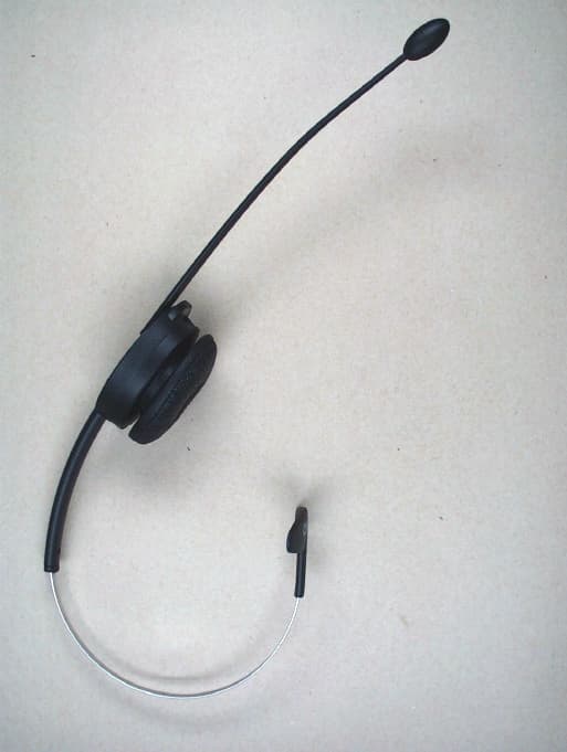
Click to zoom
Application Details
- Equipment Class
- DSS - Part 15 Spread Spectrum Transmitter
- Date of Grant
- Nov 26, 2000
- Application Purpose
- Original Equipment
- Date of Application
- Jul 20, 2000
- Equipment Note
- 2.4 GHz Cordless Telephone
- Frequency Range
- 2400.90000000 - 2482.00000000
- Company
- GN Audio USA Inc.
- Country
- United States
Documents & Files
Document Text
Text extracted from the exhibit documents filed with the FCC. Open a document above to read the original.
Users Manual
Activa 2.4 Headset User Guide 12345678 ABCDEFG Components 1. Base A. Headset/Handset Selector B. Microphone Volume Control C. Telephone Compatibility Settings D. Battery Charging Indicator E. On-Line Indicator (base) 2. Stand 3. Telephone Interface Cord 4. AC Power Adapter 5. Receiver Housing F. Ear Cushion Mounted on Earplate G. Mute Button H. Receive Volume Control Button I. On-Line Indicator (headset) 6. Adjustable Headband 7. Stabilizer 8. Flexible Microphone Boom 9. Microphone 10. Foam Cover for Microphone 6. 2. 5. 4. 3. C. 10. 7. 1. 9. 8. A. B. D. E. F. H. I. G. 77 Northeastern Blvd. • Nashua, NH 03062 USA 1-800-826-4656 • www.gnnetcom.com 54-????-A Printed in USA August 2000 Assembling1 Connect all cords. 2 Attach the base to the stand. Charging the Battery 3 Insert the headsetinto the base (eitherside can be used).The battery charg-ing indicator on thebase illuminates. 4 The headset batteryis not charged whendelivered. Place theheadset in the basefor at least 30 minutes before making the follow-ing adjustments. It takes 3 hours to fully charge thebattery. When fullycharged, the batterycharging indicatorflashes. A fullycharged battery provides 7 hours of talktime. Netcom Netcom Act-AssemblyFirst draft 7-11-00 54-???? Activa2.4 7/14/00 4:01 PM Page 1 Adjusting the Microphone Volume15 Put on the headset. 16 Press the headset/handset selectorto switch to handset mode. 17 Call someone using your handset and ask the personto help you evaluate the volume of your voice. 18 Using theheadset/handset selectorto toggle back and forthbetween handset andheadset mode, adjustthe microphone volumecontrol from 1 to 8 byfirst talking in thehandset and then in theheadset in each switch position. 19 When the person hearsno difference whetheryou talk in the handsetor headset, you have thecorrect setting. If the set-ting is 7 or 8, it may benecessary to more thetelephone compatibilitysetting to G. Checking the System5 If your telephone has volume control, set the volume in the middle position. 6 Press the headset/handsetselector to switch on theheadset. 7 The on-line indicator onthe base illuminates. 8 The on-lineindicator onthe headsetbegins flash-ing within 10seconds. Ifthe on-lineindicator doesnot flash,recheckassembly. 9 The system is now working. 10 If the lights are still off, the headset/handset selectoris in handset position. Press the headset/handsetselector once. Adjusting to your Telephone11 Put on the headset. 12 Make sure the mutefunction is off. Ifyou hear a signalevery 3 seconds, themute function is on.Turn off the mutefunction by pressingthe mute buttononce. 13 Lift the handsetfrom your telephoneand listen for a dialtone in your headset. 14 If there is no dialtone, adjust the tele-phone compatilibilitysetting until the dialtone is clear. If dialtone is clear for bothA and G, set to A. ¥1¥2¥3¥4¥5¥6¥7¥8¥A¥B¥C¥D¥E¥F¥G ¥1¥2¥3¥4¥5¥6¥7¥8¥A¥B¥C¥D¥E¥F¥G WarrantyGN Netcom, Inc. warrants this product against all defects in material and workmanship for a period of one year from the date oforiginal purchase. The conditions of this warranty and our responsibilities under this warranty are as follows: • The warranty is limited to the original purchaser.• The warranty is void if the serial number, date code label or product label is removed, or if the product has been subject to physical abuse, improper installation, modification, or repair by unauthorized third parties. • The responsibility of GN Netcom, Inc. under this warranty shall be limited to the repair or replacement of the product at the sole discretion of GN Netcom, Inc. • Any implied warranty on GN Netcom, Inc. products is limited to one year from the date of purchase on all parts, including the cords and connectors. Specifically exempt from warranty are limited-life consumable components subject to normal wear andtear, such as microphone windscreens, ear cushions, ear tips, decorative finishes, batteries, and other accessories. GN Netcom,Inc. is not liable for any incidental or consequential damages arising from the use or misuse of any GN Netcom, Inc. product. • A copy of your receipt or other proof of purchase is required. Without proof of purchase, your warranty is defined as beginnin g on the date of manufacture as labeled on the product. • This warranty gives you specific legal rights and you may have other rights which vary from state to state. Unless otherwise instructed in the User Guide, the user may not, under any circumstances, attempt any service, adjustments orrepairs on this unit, whether in or out of warranty. It must be returned to the factory or authorized service agency for all su ch work. To Obtain ServiceFor customer service and technical support, call GN Netcom, Inc. at 1-800-826-4656.If it becomes necessary to send a unit in for repair, it is not necessary to call for a Return Material Authorization (RMA) num ber, as one will be assigned upon receipt of the package at the factory.Ship the product in a suitable shipping container, fully insured and with the shipping charges prepaid. Include the following w ith the product: • Your name, company name, address and telephone number.• A description of the problem.• A copy of the receipt or other proof of purchase (without proof of purchase, your warranty will be defined as beginning on the date of manufacture as labeled on the product).Or, for out of warranty products: • A purchase order which authorizes repair. In warranty products are warranted for one year from the repair date or for the remainder of the original warranty period, whic hever is longer. Out of warranty products will be repaired or replaced at the prevailing charge and carry a one year warranty from re pair date. GN Netcom, Inc. will not assume any responsibility for any loss or damage incurred in shipping. Any repair work on GN Netcom,Inc. products by unauthorized third parties voids any existing GN Netcom, Inc. warranty. Ship To:GN Netcom, Inc. • 77 Northeastern Boulevard • Nashua, NH 03062 • 1-800-826-46…
Text truncated - open the document above for the full version.
Block Diagram
Technical Documentation Activa 2G4 Date: 2000-05-03File: Activa_desc.DOCRef.: JMRev.: 1Page: 5 of 7 page(s) This document and the information contained is property of RTX Telecom A/S, Denmark. Unauthorized copying is not allowed. The information in this document is believed to be correct at the time of writing. RTX Telecom A/S reserves the right at any time to change said content, circuitry and specifications. 2 Flow chart for the Base station. This document describes the design of the Base station. 2.1 Telephone interface: The signal from the telephone is connected to J2 and the receiver is connected to J3. With the two relays RL1 and RL2 is possible to route the signal from J2 to J3 or from J2 to the analog interface. 2.2 Gain control, Termination switch: The in/out signals from the telephone interface goes to the switch S1, where it is possible to switch between 7 different configuration of the wiring in the telephone. S3 switches the MARS system on and off. T5 is an insulation transformer. The output from the transformer is supplied to the input of the burstmode controller and the differential amplifier IC8A. The output from the 4. RF. 3. Baseband. Microcotroller. 6. Power Supply. 1 .Telephone Interface. 2. Gain Control. Termination Switch AGC. 7. Charger
Block Diagram
Technical Documentation Activa 2G4 Date: 2000-05-03File: Activa_desc.DOCRef.: JMRev.: 1Page: 3 of 7 page(s) This document and the information contained is property of RTX Telecom A/S, Denmark. Unauthorized copying is not allowed. The information in this document is believed to be correct at the time of writing. RTX Telecom A/S reserves the right at any time to change said content, circuitry and specifications. 1 Flow chart for the Remote. This document describes the design of the Base station. 1.1 Headset: The headset is connected to J5, which is integrated on the PCB. 1.2 Baseband: Microcontroller. The micro/burstmode controller IC5, is a device containing both the microcontroller and MARS digital/analog interface. The clock frequency for the microcontroller is 9.048436 MHz it is possible to tune the crystal with the capacitor diode D1 who is controlled by the microntroller. The serial interface is bi-directional interface; R16, C38 and D5 protect it for ESD and EMC. Burst Mode Controller. The burstmode controller (BMC) inside the microcontroller performs all the time critical control functions and the audio interface to the transducers. A crystal oscillator controlled by the crystal X1 generates the clock signal. The frequency is nominally 9.048436MHz, but can be tuned by the varicap diode D1, which is controlled from an analog output from the microcontroller. 3.RF.2.Baseband. 1.Microphone Ear speaker. 4. Power Supply Baseband. Batteri.
Cover Letter(s)
TIMCO ENGINEERING, INC. 849 N.W. STATE ROAD 45 P.O. BOX 370 NEWBERRY, FLORIDA 32669 PHONE: 888-472-2424 OR 352-472-5500 FAX: 352-472-2030 EMAIL: [email protected] or [email protected] November 15, 2000 Mr. Errol Chang Federal Communicatio ns Co mmission Authorization and Evaluation Division 7435 Oakland Mills Road Columbia, MD 21046 REF: GN NETCOM INC.’S FCC ID: BCEACTIVA24 CONFIRMATION #: EA98250 - YOUR CORRESPONDENCE ID # 16949 Dear Errol: With reference to correspondence ID 16949: 1. The channel separation is about 1.04MHz and the 20 dB bandwidth is about 999 kHz. I have uploaded plots. There are 79 hopping channels/frequencies. The dwell time is 440us. 2. Please refer to the block diagram of the transceiver (page 3 of 6 of the circuit description) - in which the synthesizer and voltage controlled oscillator are both shared by the transmitter and thed receiver. 3. This device is a 2.4 GHz device; section 15.247(b)(2) refers to 902-928 MHz devices so I’m not sure what the issue is. If you have any questions, please advise. Regards, Sharon A. Hoffma n/TIMCO ENGINEERING, INC. T:\CUS\G\GN\243A0\16949\EC01115LTR.doc
External Photos
ELECTRONIC TECHNOLOGY SYSTEMS DR.GENZ GMBH REGISTRATIONNUMBER: G0M20005-2224-T-42 ELECTRONIC TECHNOLOGY SYSTEMS DR. GENZ GMBH STORKOWER STR. 38C, D-15526 REICHENWALDE B. BERLINAppendix Page 7 of 9
External Photos
ELECTRONIC TECHNOLOGY SYSTEMS DR.GENZ GMBH REGISTRATIONNUMBER: G0M20005-2224-T-42 ELECTRONIC TECHNOLOGY SYSTEMS DR. GENZ GMBH STORKOWER STR. 38C, D-15526 REICHENWALDE B. BERLINAppendix Page 1 of 9 Appendix A. Pictures
ID Label/Location Info
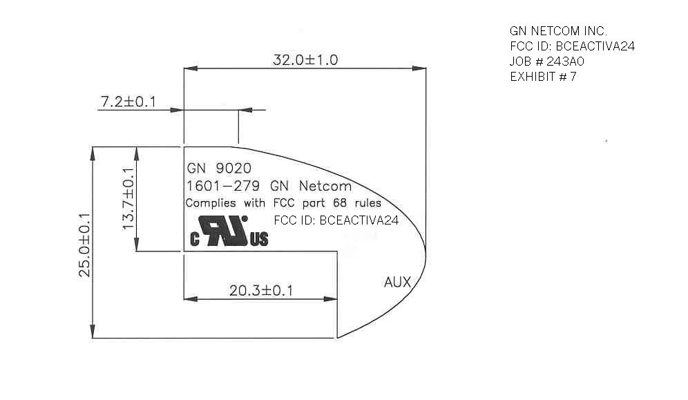
ELECTRONIC TECHNOLOGY SYSTEMS DR.GENZ GMBH REGISTRATIONNUMBER: G0M20005-2224-T-42 ELECTRONIC TECHNOLOGY SYSTEMS DR. GENZ GMBH STORKOWER STR. 38C, D-15526 REICHENWALDE B. BERLINAppendix Page 2 of 9
Internal Photos
ELECTRONIC TECHNOLOGY SYSTEMS DR.GENZ GMBH REGISTRATIONNUMBER: G0M20005-2224-T-42 ELECTRONIC TECHNOLOGY SYSTEMS DR. GENZ GMBH STORKOWER STR. 38C, D-15526 REICHENWALDE B. BERLINAppendix Page 5 of 9 ELECTRONIC TECHNOLOGY SYSTEMS DR.GENZ GMBH REGISTRATIONNUMBER: G0M20005-2224-T-42 ELECTRONIC TECHNOLOGY SYSTEMS DR. GENZ GMBH STORKOWER STR. 38C, D-15526 REICHENWALDE B. BERLINAppendix Page 6 of 9
Internal Photos
ELECTRONIC TECHNOLOGY SYSTEMS DR.GENZ GMBH REGISTRATIONNUMBER: G0M20005-2224-T-42 ELECTRONIC TECHNOLOGY SYSTEMS DR. GENZ GMBH STORKOWER STR. 38C, D-15526 REICHENWALDE B. BERLINAppendix Page 8 of 9 ELECTRONIC TECHNOLOGY SYSTEMS DR.GENZ GMBH REGISTRATIONNUMBER: G0M20005-2224-T-42 ELECTRONIC TECHNOLOGY SYSTEMS DR. GENZ GMBH STORKOWER STR. 38C, D-15526 REICHENWALDE B. BERLINAppendix Page 9 of 9
Operational Description
Technical Documentation RF part Activa 2G4(SUBJECT) Date: 2000-05-03File: Activa_rf_part.docRef.: JMRev.: 1Page: 1 of 6 page(s) This document and the information contained is property of RTX Telecom A/S, Denmark. Unauthorized copying is not allowed. The information in this document is believed to be correct at the time of writing. RTX Telecom A/S reserves the right at any time to change said content, circuitry and specifications. Circuit Description for the RF part Technical Documentation RF part Activa 2G4(SUBJECT) Date: 2000-05-03File: Activa_rf_part.docRef.: JMRev.: 1Page: 2 of 6 page(s) This document and the information contained is property of RTX Telecom A/S, Denmark. Unauthorized copying is not allowed. The information in this document is believed to be correct at the time of writing. RTX Telecom A/S reserves the right at any time to change said content, circuitry and specifications. 1 Overview 1.1.1The Receive path3 1.1.2The Frequency Synthesizer part4 1.1.3The TX path4 2VCO circuit4 3Doubler filter and Buffer amplifier4 4Buffer amplifier with control circuit5 5TX/RX switch5 6Receiver Front End5 7IF and demodulator circuit5 8Data Slicer6 Technical Documentation RF part Activa 2G4(SUBJECT) Date: 2000-05-03File: Activa_rf_part.docRef.: JMRev.: 1Page: 3 of 6 page(s) This document and the information contained is property of RTX Telecom A/S, Denmark. Unauthorized copying is not allowed. The information in this document is believed to be correct at the time of writing. RTX Telecom A/S reserves the right at any time to change said content, circuitry and specifications. This document describes the functionality of the RF part of Activa. The RF is based on the LMX 3162 single chip RF from National Semiconductor. Two to other main components are the ALPS UREA630 VCO. SAW Filter 110.6 MHz QUAD VOLTAGE CONTROLLED OSCILLATOR TRADAT PLLLE PLLDAT PLLCLK RFON RECPD CMPREF RFCLK RSSI RECDAT QUAD_ TUNE PAON TRSWIT TR-SWITCH VBAT LNA TR-SWITCH T/R Buffer DOUBLER BP- Filter BP- Filter MIXER PLL LOGIC IF AMPLIFIER VBAT_FILT 1.1.1 The Receive path The receiver is a single conversion receiver with an IF frequency centered at 110.592 MHz. From the antenna the signal pass through a low loss ceramic filter and a TX/RX switch. After amplification in a bipolar LNA and further filtering in ceramic filter the signal is downconverted in a mixer in the LMX3162. A SAW filter is used after the mixer to perform the channel selection filtering. An limiter discriminator demodulator is used. After the demodulation the signal is filtered. The detection is performed with a comparator. Technical Documentation RF part Activa 2G4(SUBJECT) Date: 2000-05-03File: Activa_rf_part.docRef.: JMRev.: 1Page: 4 of 6 page(s) This document and the information contained is property of RTX Telecom A/S, Denmark. Unauthorized copying is not allowed. The information in this document is believed to be correct at the time of writing. RTX Telecom A/S reserves the right at any time to change said content, circuitry and specifications. 1.1.2 The Frequency Synthesizer part The frequency synthesizer consists of a VCO operating at half the wanted frequency controlled by an synthesizer in the LMX 3162. The VCO signal is doubled in a doubler in the LMX 3162 and split to the TX buffer and as LO signal for the receiver mixer. The TX modulation is performed as open loop modulation on the VCO. 1.1.3 The TX path The signal from the doubled is amplified in a bipolar transistor buffer. The final amplification is performed by the buffer T108. The burst control is performed by an PNP transistor. After the PA the TX signal is feed through the TX/RX switch and the antenna filter. 2 VCO circuit The VCO is a band switch VCO from ALPS (UREA630). To avoid frequency drift and offset when the PA is turned on a separate 3.0 voltage regulator (LP2980) is used. The VBAT and VBAT_2 voltage typical drops 0.1 – 0.2 V when the PA is on. The band switch signal (VCO_BND) is used to switch the VCO between RX (1172.8437 – 1213.1529 MHz ) and TX (1200.4917 – 1240.8009 MHz). It is important that there is no voltage jump on the VCO_BND signal when the PA is turned on, as this will cause frequency drift. The voltage on the CTR pin of the VCO determines the frequency of the VCO. This voltage comes from the synthesizer output and is filtered in the loop filter. The used loop filter (C140=680pF,C141=2.2nF and R118=3.3kΩ) ensures that the lock time for the synthesizer is short (approx. 50 μs-100μs). The VCO uses the open loop modulation scheme. This means that during transmission of a burst is the synthesizer powered down and the loop voltage is only hold by the capacitors in the loop filter. Due to this it is important that there is no leakage current in the capacitors. This can be fulfilled by using NP0 type capacitors. In the open loop state, the modulation signal (TRADAT) is injected on the MOD pin of the VCO. The MOD signal shall have the same DC value during lock in as during the transmission burst. The TRADAT signal is gaussian shaped from the BMC. It is also possible to adjust the amplitude of the TRADAT signal in the BMC. 3 Doubler filter and Buffer amplifier The primary purpose of the doubler filter (C159, L4) is to remove the fundamental frequency of the frequency doubled signal. Also the 3 rd harmonic of the VCO frequency is attenuated. The attenuation at 900 MHz is around 25dB and the attenuation at 2.8GZ is approx. 10 dB. The filter is designed as a wideband filter with a pass band of approx. 1.5- 2.0 GHz. This is to ensure that the attenuation of the wanted signal at 1880-1930 MHz is less than approx. 1dB taking worst case parameters into account. The buffer amplifier (T108) has a collector current of 7mA and 7-8dB of small signal gain. The transistor is driven into saturation and gives approx. +2 dBm of output power. This signal is feed directly to the output. The buffer and doubler are turned on during the blind slot before the burst to avoid any pulling of the VCO T…
Text truncated - open the document above for the full version.
Operational Description
Technical Documentation Activa 2G4 Date: 2000-05-03File: Activa_desc.DOCRef.: JMRev.: 1Page: 1 of 7 page(s) This document and the information contained is property of RTX Telecom A/S, Denmark. Unauthorized copying is not allowed. The information in this document is believed to be correct at the time of writing. RTX Telecom A/S reserves the right at any time to change said content, circuitry and specifications. Flow Chart and technical description Activa Remote & Base Station Technical Documentation Activa 2G4 Date: 2000-05-03File: Activa_desc.DOCRef.: JMRev.: 1Page: 2 of 7 page(s) This document and the information contained is property of RTX Telecom A/S, Denmark. Unauthorized copying is not allowed. The information in this document is believed to be correct at the time of writing. RTX Telecom A/S reserves the right at any time to change said content, circuitry and specifications. Table of contents. 1Flow chart for the Remote........................................................................3 1.1Headset:......................................................................................................................3 1.2Baseband:...................................................................................................................3 1.3RF: See “Circuit description for the RF part”..............................................................4 1.4Power supply baseband:..............................................................................................4 2Flow chart for the Base station.................................................................5 2.1Telephone interface:...................................................................................................5 2.2Gain control, Termination switch:...............................................................................5 2.3Baseband, Microcontroller:.........................................................................................6 2.4RF: See “Circuit description for the RF part”..............................................................7 2.5Power supply:.............................................................................................................7 2.6Charger:......................................................................................................................7 Technical Documentation Activa 2G4 Date: 2000-05-03File: Activa_desc.DOCRef.: JMRev.: 1Page: 3 of 7 page(s) This document and the information contained is property of RTX Telecom A/S, Denmark. Unauthorized copying is not allowed. The information in this document is believed to be correct at the time of writing. RTX Telecom A/S reserves the right at any time to change said content, circuitry and specifications. 1 Flow chart for the Remote. This document describes the design of the Base station. 1.1 Headset: The headset is connected to J5, which is integrated on the PCB. 1.2 Baseband: Microcontroller. The micro/burstmode controller IC5, is a device containing both the microcontroller and MARS digital/analog interface. The clock frequency for the microcontroller is 9.048436 MHz it is possible to tune the crystal with the capacitor diode D1 who is controlled by the microntroller. The serial interface is bi-directional interface; R16, C38 and D5 protect it for ESD and EMC. Burst Mode Controller. The burstmode controller (BMC) inside the microcontroller performs all the time critical control functions and the audio interface to the transducers. A crystal oscillator controlled by the crystal X1 generates the clock signal. The frequency is nominally 9.048436MHz, but can be tuned by the varicap diode D1, which is controlled from an analog output from the microcontroller. 3.RF.2.Baseband. 1.Microphone Ear speaker. 4. Power Supply Baseband. Batteri. Technical Documentation Activa 2G4 Date: 2000-05-03File: Activa_desc.DOCRef.: JMRev.: 1Page: 4 of 7 page(s) This document and the information contained is property of RTX Telecom A/S, Denmark. Unauthorized copying is not allowed. The information in this document is believed to be correct at the time of writing. RTX Telecom A/S reserves the right at any time to change said content, circuitry and specifications. There are 3 different supply inputs on the BMC, one for the digital circuits (VDD), one for the analog circuits of the RF interface (AVD) and one for the analog part of the codec (AVD2). The two analog supplies have been decoupled separately to reduce the noise levels. The interface to the transducers (microphone and earspeaker) consists of an audio codec placed internally in the BMC. The microphone in the Activa is an electret type, which requires a supply current. Both speaker output and microphone input is decoupled with 5p6 capacitors. This value is chosen because it has low impedance at 2.4GHz. When the handset is in standby the VREF outputs will be powered down, so that the microphone will consume no power in this mode. The earspeaker is coupled differentially to the loudspeaker outputs LRS+ and LRS-. 1.3 RF: See “Circuit description for the RF part”. 1.4 Power supply baseband: Because the Activa is powered by 1 cell, a step-up converter is needed. This is done by IC1 this is an integrated circuit that contains all what is needed for a step-up converter, only an external coil is needed. R9 and R22 set the output voltage (3.7V). The 3.7V power is supplied to the RF part and the baseband controller IC5. This device contains a low drop regulator, only an external PnP transistor is needed (T2). The regulated output voltage from the regulator IC5 is 2.85V. When the input voltage is below a threshold voltage determined by IC1 the switch regulator will be turned off, resulting in a current consumption of less than 5uA to protect the batteries against deep discharge. R1 and C4 generate the reset pulse delay. Technical Documentation Activa 2G4 Date: 2000-05-03File: Activa_desc.DOCRef.: JMRev.: 1Page: 5 of 7 page(s) This document and the information contained i…
Text truncated - open the document above for the full version.
Operational Description
Technical Documentation MARS 2G4 Freq. Hopping Specification File hopping algorithms Date 2000-10-10 Revision 0.4 Ref. JTP/FMPage 1 of 9 This document and the information contained is property of RTX Telecom A/S, Denmark. Unauthorized copying is not allowed. The information in this document is believed to be correct at the time of writing. RTX Telecom A/S reserves the right at any time to change said content, circuitry and specifications. Preliminary MARS 2.4GHz Frequency hopping and Dual slot diversity description History Ver 0.1JTP980909 Initial version Ver 0.2FM990111 Updated/changed for type approval Ver 0.3FM990204 Updated/changed for type approval with new crystal Ver 0.4 FM 990730 Updated/New frequencies /new delay Ver 0.5 FM 990909 Updated/New frequencies Technical Documentation MARS 2G4 Freq. Hopping Specification File hopping algorithms Date 2000-10-10 Revision 0.4 Ref. JTP/FMPage 2 of 9 This document and the information contained is property of RTX Telecom A/S, Denmark. Unauthorized copying is not allowed. The information in this document is believed to be correct at the time of writing. RTX Telecom A/S reserves the right at any time to change said content, circuitry and specifications. HISTORY ........................................................................................................................................................................1 1.INTRODUCTION .................................................................................................................................................3 2.AVOIDANCE METHOD .....................................................................................................................................3 2.1K NOWN HOPPERS.................................................................................................................................................3 2.2M ICROWAVE OVENS............................................................................................................................................3 2.3CW INTERFERENCE ON FIXED RF CARRIERS........................................................................................................3 2.4O THER HOPPERS..................................................................................................................................................3 2.5I MPROVE RANGE / MULTI-PATH PERFORMANCE...................................................................................................3 3.ADAPTATION TO 2.4GHZ ISM BAND ............................................................................................................4 3.1F RAME FORMAT:..................................................................................................................................................4 3.2B URST FORMAT: ..................................................................................................................................................5 3.2.1Sync-field...................................................................................................................................................5 3.2.2A-field ........................................................................................................................................................5 3.2.3B-field ........................................................................................................................................................6 3.2.4XZ-field......................................................................................................................................................6 3.3F REQUENCY HOPPING ALGORITHM......................................................................................................................7 3.3.1Excluded carriers ......................................................................................................................................7 3.3.2Hopping tables ..........................................................................................................................................7 3.3.3Example.....................................................................................................................................................8 3.4PP SYNCHRONIZATION PROCEDURE.....................................................................................................................8 3.5D UAL SLOT DIVERSITY.........................................................................................................................................9 3.6P OWER AMPLIFIER ACTIVATION...........................................................................................................................9 3.6.1External connection...................................................................................................................................9 3.6.2Internal connection ...................................................................................................................................9 Technical Documentation MARS 2G4 Freq. Hopping Specification File hopping algorithms Date 2000-10-10 Revision 0.4 Ref. JTP/FMPage 3 of 9 This document and the information contained is property of RTX Telecom A/S, Denmark. Unauthorized copying is not allowed. The information in this document is believed to be correct at the time of writing. RTX Telecom A/S reserves the right at any time to change said content, circuitry and specifications. 1. Introduction The Mars system is based on DECT the ETSI standard ETS-300-175-1 to ETS-300-175-9. The Mars system is improved by implementing extra features to combat the interference at 2.4 GHz. The frequency hopping method for 2.4 GHz ISM band has to provide optimal performance and connection quality in environment with 5 different types of interference: 1. Other interference of MARS-type, known hopping algorithm and avoidance method (synchronized/unsynchronized). 2. Microwave ovens, sweeping the most of the …
Text truncated - open the document above for the full version.
Operational Description
Technical Documentation RF part Activa 2G4(SUBJECT) Date: 2000-05-03File: Activa_rf_part.docRef.: JMRev.: 1Page: 1 of 6 page(s) This document and the information contained is property of RTX Telecom A/S, Denmark. Unauthorized copying is not allowed. The information in this document is believed to be correct at the time of writing. RTX Telecom A/S reserves the right at any time to change said content, circuitry and specifications. Circuit Description for the RF part Technical Documentation RF part Activa 2G4(SUBJECT) Date: 2000-05-03File: Activa_rf_part.docRef.: JMRev.: 1Page: 2 of 6 page(s) This document and the information contained is property of RTX Telecom A/S, Denmark. Unauthorized copying is not allowed. The infor…
Text truncated - open the document above for the full version.
Contact Information
Applicant
Steen Kaiser(Manager, Product Certifications)
Technical Contact
Timco Engineering, Inc.Eric F Dobson
[email protected]888-472-2424
P.O. Box 370 · Newberry, Florida · United States
Non-Technical Contact
Timco Engineering, Inc.Eric F Dobson
[email protected]888-472-2424
Test Firm
Timco Engineering, Inc.S Sanders
Technical Specifications
| # | Rule Parts | Frequency Range | Power Output |
|---|---|---|---|
| 1 | 15C | 2.40 GHz - 2.48 GHz | 3.00 mW |
Other Applications from GN Audio USA Inc.
BCE-OTE995
Aug 19, 2026Bluetooth Headset
Equipment Class
DSS - Part 15 Spread Spectrum TransmitterBCE-HSC240W
Aug 07, 2026Bluetooth Headset
Equipment Class
DSS - Part 15 Spread Spectrum TransmitterBCE-HSC260W
Aug 04, 2026Bluetooth Headset
Equipment Class
DTS - Digital Transmission SystemBCE-OTE800
Mar 24, 2026OTE985 Bluetooth Headset
Equipment Class
DTS - Digital Transmission SystemBCE-OTE810
Mar 19, 2026OTE985 Bluetooth Headset
Equipment Class
DSS - Part 15 Spread Spectrum Transmitter