DCP7FGAERPIR1
Alarm Electronics Manufacturing Co Inc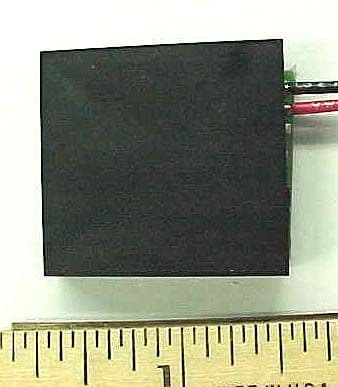
Click to zoom
Application Details
- Equipment Class
- DSC - Part 15 Security/Remote Control Transmitter
- Date of Grant
- Feb 09, 2000
- Application Purpose
- Original Equipment
- Date of Application
- Nov 15, 1999
- Frequency Range
- 303.75000000 - 304.25000000
- Country
- United States
Documents & Files


Document Text
Text extracted from the exhibit documents filed with the FCC. Open a document above to read the original.
Attestation Statements
STATEMENT OF MICHAEL A. NICOLAY In Connection With APPLICATION FOR CERTIFICATION SECURITY ALARM TRANSMITTER FCC ID: DCP7FGAEPIR1 I am an Engineer, an employee in the firm of Carl T. Jones Corporation, with offices located in Springfield, Virginia. My education and experience are a matter of record with the Federal Communications Commission. All of the measurements contained in this test report were performed by me or under my supervision, and I attest to the accuracy of each. I submit that, to the best of my knowledge, the test sample meets the technical standards set forth in the Commission's Part 15 Rules and Regulations. DATED: November 3, 1999 Michael A. Nicolay Carl T. Jones Corporation 7901 Yarnwood Court Springfield, VA 22153 (703) 569-7704 [email protected]
Attestation Statements
This Category not applicable for this application .
Cover Letter(s)
STATEMENT OF MICHAEL A. NICOLAY In Connection With APPLICATION FOR CERTIFICATION SECURITY ALARM TRANSMITTER FCC ID: DCP7FGAEPIR1 I am an Engineer, an employee in the firm of Carl T. Jones Corporation, with offices located in Springfield, Virginia. My education and experience are a matter of record with the Federal Communications Commission. All of the measurements contained in this test report were performed by me or under my supervision, and I attest to the accuracy of each. I submit that, to the best of my knowledge, the test sample meets the technical standards set forth in the Commission's Part 15 Rules and Regulations. DATED: November 3, 1999 Michael A. Nicolay Carl T. Jones Corporation 7901 Yarnwood Court Springfield, VA 22153 (703) 569-7704 [email protected]
Operational Description
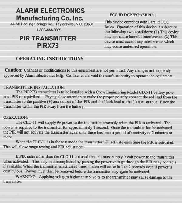
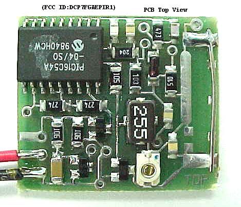
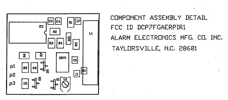
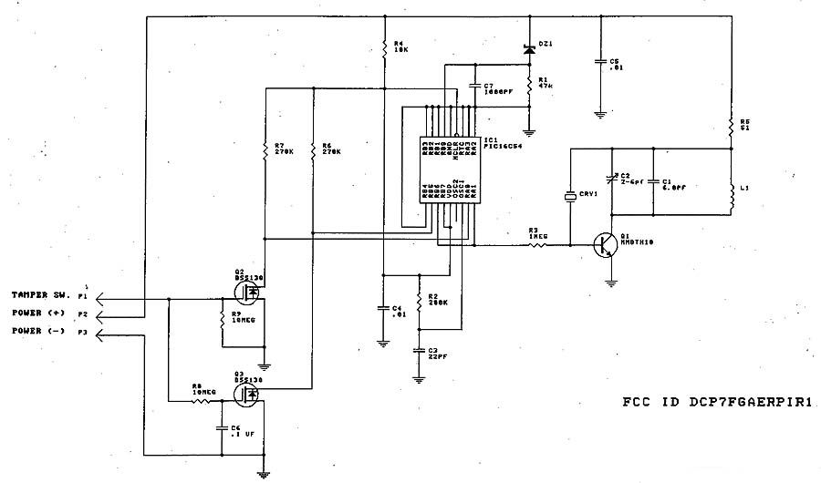
APPLICATION FOR CERTIFICATION: MODEL PIR and PIRX73 TRANSMITTER TECHNICAL REPORT FCC ID DCP7FGAERPIR1 Name and address of Applicant:Prepared By: Alarm Electronics Manufacturing Co. Inc.Edgar L. Bonner 44 All Healing Springs Road Taylorsville N. C. 28681 Ph. (828) 632-3365 Installation and Operating Instructions: A copy of the Model SMK95 “Installation and Operating Instructions” is attached to this report. DESCRIPTION OF CIRCUIT FUNCTIONS: POWER SOURCE:9V Battery GENERAL OPERATION: The PIRD73A is intended for use with receivers: FCC ID DCP7FG800, DCP7FGAER902L, DCP7FGAER904L, DCP7FG811 The format of the transmission is compatible with the receivers. The PIR73A is an auxiliary transmitter for use in security alarm systems. It is designed to be used with devices such as battery powered passive inferred motion detectors with internal 9 volt battery power sources and having switched voltage or relay outputs and tamper switches. There is no power drain from the battery power source until such time as the transmitter is activated. The transmitter has a built in timer program which limits output transmission to less than 3 seconds. The transmitter is expected to be activated during alarm conditions or when the tamper protection is violated. The transmitter is activated by applying voltage to the input power. The transmitter will then transmit the alarm signal until power is removed or the internal 3 second timer expires. When the transmitter is activated the input circuit is checked to determine if the activation is a result of tamper switch operation or restore and also checks the status of the 9 volt battery. All transmissions from the device are of identical format except that certain bits are set to “1" or “0" to indicate “Low Battery”, “Alarm”,and/or “Tamper”. CIRCUIT OPERATION DETAIL Referring to the schematic diagram: The input voltage is supplied to the circuit via input P3 (-) and P 2 (+) of the input circuit. The detector will apply power to the transmitter under conditions of alarm, tamper activation, and tamper restore. When the tamper switch is activated the voltage input P1 is supplied as an input simultaneously with the application of input power. The tamper input voltage remains present as long as the tamper switch is activated. When a tamper restore occurs the power is applied to the transmitter at the same time the tamper voltage is removed. An alarm condition causes the power to be applied to the transmitter without tamper voltage input. The tamper input voltage is applied to the two MOS FET devices Q2 and Q3. When the tamper voltage is first applied Q2 will turn on immediately and the turn on of Q3 will be delayed because of the RC time constant R8C6. Therefore upon initial power input RB5=0 and RA0=1 is the state of logic input to the encoder which indicates a tamper activation. When tamper voltage is removed Q2 Will turn off immediately and Q3 will be delayed. Therefore RB5=1 and RA0=0 is the logic state indicating tamper restore. With no tamper voltage present before or during activation of the power input the logic states of both RB5 and RA0 will be “1" indicating and alarm condition. Resistor R4 is a series voltage drop resistor with a value such that the 9 volt supply is lowered to approx. 5 volts at the processor input. C4 is the encoder power supply filter. R2 and C3 form RC network which sets the clock frequency for the encoder. DZ1 is a 6.2 v zener diode through which the battery voltage is monitored. When the applied input voltage is below the zener diode voltage plus the encoder trip voltage (approx 1 volt) a “Low battery” condition is detected at the encoder input RB0 and the transmitter will set the low battery flag bit in the transmitted data stream. The encoder generates the serial digital data output on pin RA1. This digital data is applied to the input of the RF stage transistor Q1 via resistor R3. The RF section consists of a crystal oscillator where the primary tuning element L1 is also the primary radiating element (antenna) of the transmitter.. Capacitors C1 and C2 tune the resonant circuit to the same frequency as the crystal CRY1 which is in the feedback loop. The frequency of operation is thereby determined by the crystal frequency. The crystal is a two port SAW type device. The transmitter is aligned at the factory and there are no provisions for user adjustment of the operating frequency. The digital output of the encoder is applied to the base of transistor Q1. This causes the RF to be gated on and off with the digital output of the encoder. The encoder limits the duration of the output transmission to 3 seconds after which the voltage input to transistor Q1 is stopped. In practice the duration of transmission is limited by the period of the voltage output from the detector which is in the order of 1 second. The time is minimized to prolong battery life.
Parts List/Tune Up Info
APPLICATION FOR CERTIFICATION: MODEL PIR and PIRX73 TRANSMITTER FCC ID DCP7FGAERPIR1 PARTS LIST PART IDDESCRIPTIONVALUE/PART NO. R1Resistor 1/8w 47k R2Resistor 1/8w200k R3Resistor 1/8w1 meg R4Resistor 1/8w10k R5Resistor 1/8w51 ohm R6Resistor 1/8w270k R7Resistor 1/8w270k R8Resistor 1/8w10 meg R9Resistor 1/8w10 meg C1Capacitor, Ceramic6.8 pf C2Capacitor, Variable 2 - 6 pf C3Capacitor, Ceramic22 pf C4Capacitor, Ceramic.01 mF C5Capacitor, Ceramic.01 mF C6Capacitor, Ceramic.1 mF Q1Transistor, NPNMMBTH10 Q2Transistor, MOS FET BSS138 Q3Transistor, MOS FETBSS138 CRY1Crystal SAW resonatorRO2104A IC1Integrated Circuit16C54A L1Inductor.9" #22ga buss wire DZ1Zener DiodeTZM5234B
Parts List/Tune Up Info
TUNEUP PROCEDURE This device is factory adjusted, the end user cannot tune or re-tune the device. For more details, see the “Operational Description” exhibit in this application.
Test Report
TABLE 1 FIELD STRENGTH RADIATED EMISSIONS DATA SHEE T ANTENNA FACTORRCL 1993/1 EMISSIONANTENN AEMISSIONANDEMISSIONLIMIT FREQUENC YPOLARITYLEVELCABLE LOSSLEVEL(3 METERS) (MHz) (H,V)(dBuV)(dB)(dBuV/m)(dBuV/m) 304.00V49.0+23.2=72.275.7 304.00H42.5+23.2=65.775.7 608.00V7.0+31.1=38.145.6 608.00H<5.5+31.1=<36.645.6 912.00V<2.0+36.2=<38.245.6 912.00H<1.5+36.2=<37.745.6 1,216.00H&V<16.5+26.0=<42.555.1** 1,520.00H&V<14.2+28.3=<42.555.1** 1,824.00H&V<13.5+29.5=<43.055.1** 2,128.00H&V<11.2+31.8=<43.055.1** 2,432.00H&V<11.0+32.2=<43.255.1** 2,736.00H&V<9.8+34.3=<44.155.1** 3,040.00H&V<9.9+35.5=<44.555.1** ALL MEASUREMENT DATA REPORTED IN PEAK . Limits specified in Average. ** 1 Meter Limit NOTE: 75.7 dBuV/m = 100uW EIRP @ 3 Meters 45.6 dBuV/m = 0.1uW EIRP @ 3 Meters CLIENT:ALARM ELECTRONICS FCC ID:DCP7F6AERPIR1 MODEL:PIR TEST DATE:08/22/99 TEST ENGINEER: Michael A. Nicolay
Test Report
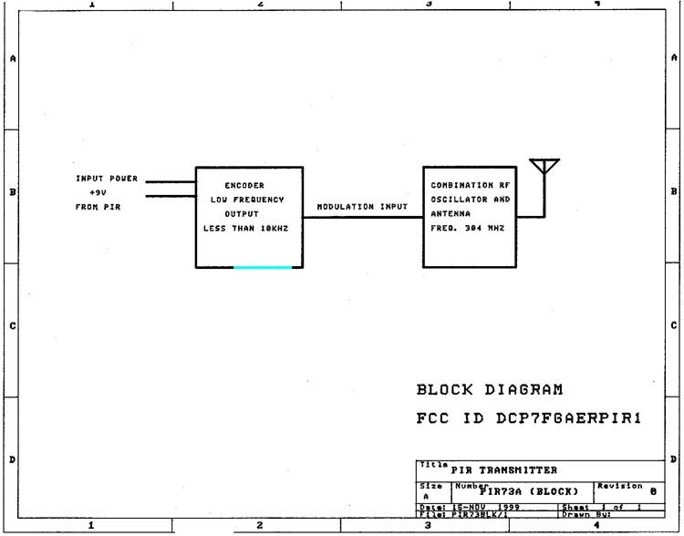
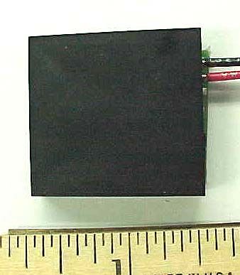
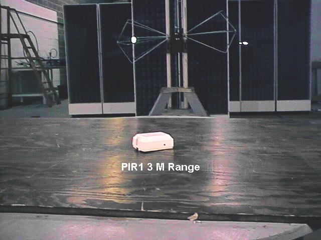
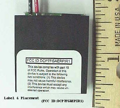
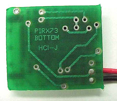
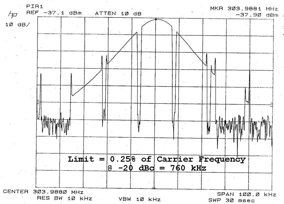
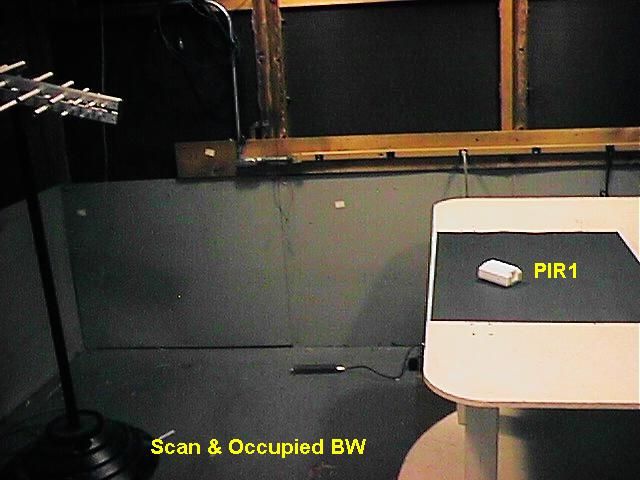
FCC ID: DCP7FGAEPIR1 1 CERTIFICATION APPLICATION I. INTRODUCTION This measurement report is submitted in support of an Application for Certification in accordance with Part 2, Subpart J and Part 15, Subpart C (effective 6/23/89) of the Federal Communications Commission's Rules and Regulations. The equipment under test (EUT) is a low power SECURITY ALARM RF transmitter. This transmitter operates at a fixed frequency of 304 MHz +/- 250 kHz and is powered by one 9 Volt battery. It is identified as either Model PIRX73 or Model PIR Transmitter (FCC ID:DCP7FGAEPIR1). Operation under the transition provisions of Paragraph 15.37 is not requested for this device. The measurements contained in this application demonstrate compliance with the limitations in effect since 6/23/89. II. INFORMATION REQUIRED FOR CERTIFICATION Paragraph(s) 2.1033(a)This application for certification is filed on FCC Form 731 with all questions answered. An application fee of $940.00 was payed. 2.1033(b)(1)The full name and mailing address of the manufacturer of the device and applicant for certification is: Alarm Electronics Manufacturing Company, Inc. 44 All Healing Springs Rd. Taylorsville, NC 28681 (2)The FCC Identifier of the device is 7FGAEPIR1. (3)A copy of the installation and operating instructions to be furnished to the user is included in the exhibits section of this application. (4)The transmitter is a SECURITY ALARM unit and is powered by one 9 Volt transistor battery. FCC ID: DCP7FGAEPIR1 2 It is designed to operate in the frequency of 304 MHz MHz +/- 250 kHz. Complete circuit schematics are provided in the exhibits section of this application. (5)A block diagram of the device is included in the appropriate exhibits section of this application. (6)A report of measurements is included in this report. (7)Photographs of this device showing the label placement, chassis assembly, and circuit layout are included in the exhibits section of this application. An digitized sample of the label is included. (8)This equipment is a stand-alone unit. No peripherals or accessories are involved. (9)Certification under the transition provisions of Paragraph 15.37 is not being requested for this device. (10)N/A. III. GENERAL TEST CONDITIONS AND PROCEDURES Measurement procedures were used as outlined in ANSI C63.4-92, as specified in Part 15.31, except as noted herein. The open field tests were performed on a three-meter range maintained by Carl T. Jones Corporation at the Springfield facility. Complete description and measurement data for the site have been placed on file with the Commission, Registration # 90490. Carl T. Jones Corporation is listed by the FCC as a facility available to do measurement work for others on a contract basis. Prior to open-field testing, the equipment was placed in a shielded enclosure and scanned at a close distance to determine its emission characteristics. IV. RADIATED EMISSION MEASUREMENTS The transmitter was assembled on a rotatable wooden test stand approximately 0.8 meters in height. FCC ID: DCP7FGAEPIR1 3 The transmitter's antenna was fully extended. The emission spectrum was examined up to 1000 MHz using a Hewlett-Packard 8568B spectrum analyzer and Compliance Design "Roberts" tuned dipole antennas. At each emission frequency, the EUT was rotated 360 degrees, and the antenna was raised and lowered from one to four meters to determine the maximum emission levels. Measurements were taken using both horizontal and vertical antenna polarizations. The spectrum analyzer's 6 dB bandwidth was set to 100 kHz. The analyzer was operated in the peak detection mode for measurements of emissions less than 1000 MHz. No post-detector video filters were used. The highest emission amplitudes relative to the appropriate limit were measured and have been recorded in Table 1. All emissions not reported were more than 20 dB below the specified limit. The actual field intensity in decibels above one microvolt per meter (dBuV/m) is determined by algebraically adding the measured level in dBuV, the antenna factor (dB), and the cable loss (dB) at the appropriate frequency. FI a (dBuV/m) = FI m (dBuV) + AF (dB) + CL (dB) FI a = Actual Field Intensity FI m = Measured Field Intensity AF = Antenna Factor CL = Cable Loss As a sample calculation, assume a particular device emits a signal with a frequency of 49.86 MHz. The maximized received signal level measured as 69.4 dB μ V. The total attenuation factor (antenna factor plus cable loss) for 49.86 MHz is 4.8 dB. The actual radiated field is calculated as follows: 69.4 dB μ V + 4.8 dB = 74.2 dBuV/m or 5,128.6 μ V/m (peak) The field strength of the fundamental did not exceed the authorized field strengths (average) at 3 meters, as specified in Paragraph 15.231(b). FCC ID: DCP7FGAEPIR1 4 All other emissions were found to be in compliance with the restrictions of Paragraph 15.231(b) of the Commission's Rules. Because the emissions were below the limits using peak detection, average detection and duty cycle correction factors were not calculated. V. OCCUPIED BANDWIDTH MEASUREMENTS In order to demonstrate compliance with the occupied bandwidth restrictions of Paragraph 15.231(c), the occupied bandwidth of the EUT was measured. Paragraph 15.231(b) specifies that the occupied bandwidth cannot exceed 0.25% of the center frequency as measured 20 dB down from the modulated carrier. The allowed occupied bandwidth for this device is 760 kHz. One spectral plot is included with a resolution bandwidth (RBW) adjusted to 10 kHz, as per the recommendation of Mr. Greg Czumak. This plot demonstrate compliance with the requirements of Paragraph 15.231(c). VI. POWER LINE CONDUCTED EMISSIONS MEASUREMENTS Measurements of the power line conducted emissions were not performed since the EUT has no means for connection to the public power utility grid. VII. Periodic Operation in the band above 70 MHz (15.231) The equipment under test is a motion detector. The device triggers the carrier on when an i…
Text truncated - open the document above for the full version.
Contact Information
Applicant
Edgar L Bonner(President)
828 632-3365
Technical Contact
Carl T. Jones CorporationMichael A Nicolay
[email protected]703-569-7704
7901 Yarnwood Court · Springfield, Virginia · United States
Non-Technical Contact
Carl T. Jones CorporationMichael A Nicolay
[email protected]703-569-7704
Technical Specifications
| # | Rule Parts | Frequency Range | Power Output |
|---|---|---|---|
| 1 | 15C | 303.75 MHz - 304.25 MHz | - |
Other Applications from Alarm Electronics Manufacturing Co Inc
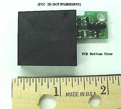
DCP7FGAERSK95
Feb 09, 2000Smoke Detector TX
Equipment Class
DSC - Part 15 Security/Remote Control Transmitter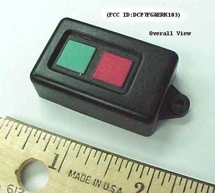
DCP7FGAERK103
Feb 09, 2000Key Code Security Alarm TX
Equipment Class
DSC - Part 15 Security/Remote Control Transmitter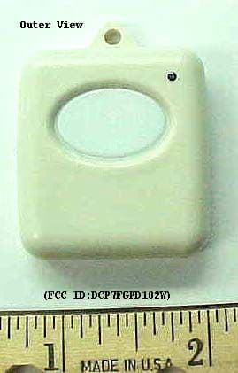
DCP7FGPD102W
Feb 09, 2000DSC - Part 15 Security/Remote Control Transmitter
Equipment Class
DSC - Part 15 Security/Remote Control Transmitter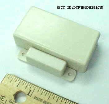
DCP7FGDW101CW
Feb 09, 2000DSC - Part 15 Security/Remote Control Transmitter
Equipment Class
DSC - Part 15 Security/Remote Control TransmitterDCP7FGAER904L
Dec 02, 1997Security System Receiver
Equipment Class
CYY - Communications Receiver used w/Pt 15 Transmitter