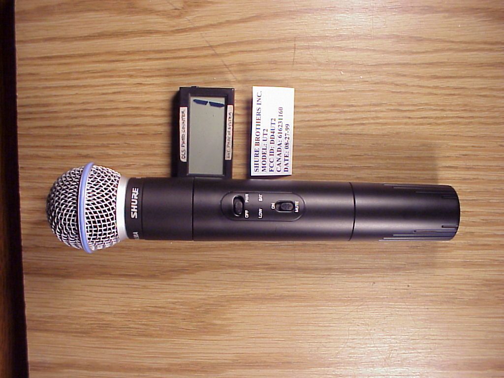
DD4UT2BLow Power Handheld TX
Shure Incorporated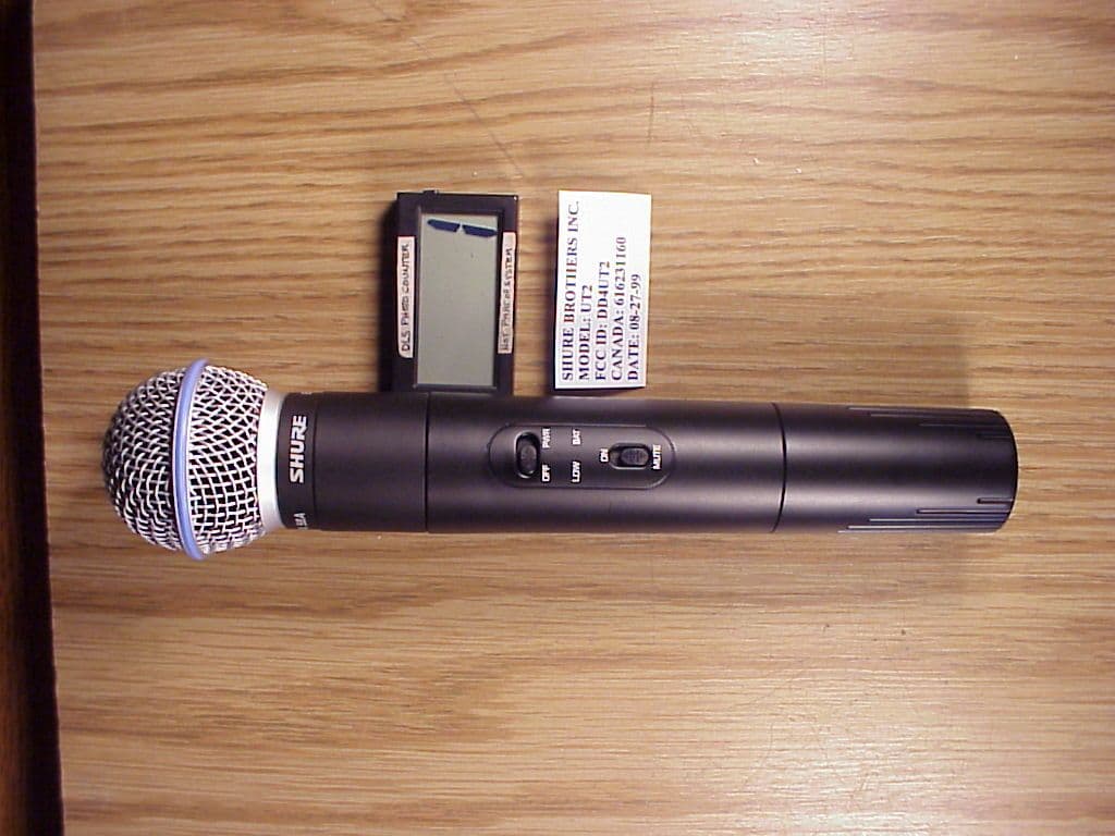
Click to zoom
Application Details
- Equipment Class
- TNF - Licensed Non-Broadcast Transmitter Held to Face
- Date of Grant
- Jan 23, 2000
- Application Purpose
- Original Equipment
- Date of Application
- Oct 05, 1999
- Equipment Note
- Low Power Handheld TX
- Frequency Range
- 740.00000000 - 752.00000000
- Company
- Shure Incorporated
- Country
- United States
Documents & Files
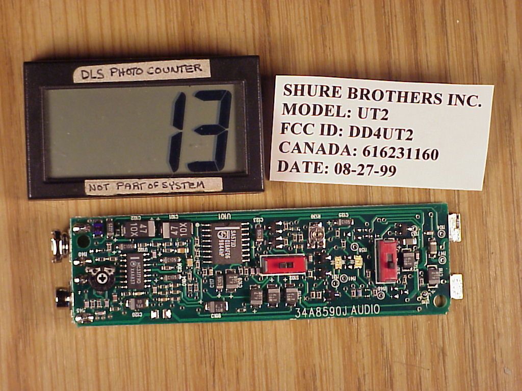
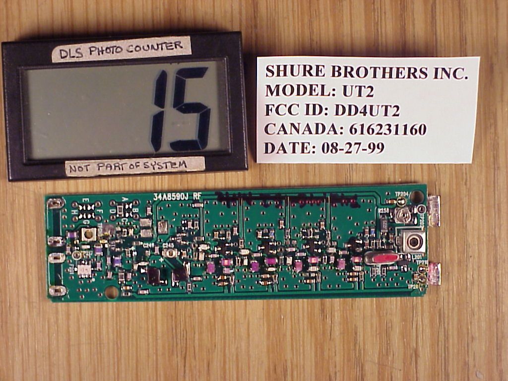
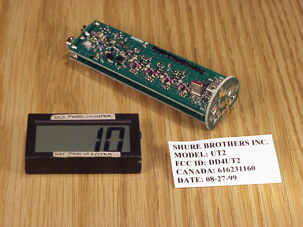
Document Text
Text extracted from the exhibit documents filed with the FCC. Open a document above to read the original.
Users Manual
1 UT S ER IES ENGLISH THE TWO MINUTE USER’S GUIDE 2:00 The instructions on this page will help you get your UT Series system up and running in minutes. For more detailed instructions, read the section of this manual that applies to your system. RECEIVER SETUP 1. Connect the supplied ac power adapter to the DC INPUT connector on the back of the receiver. Insert the adapter’s cable into the power cable retainer on the bottom of the unit. Plug the adapter into a wall socket or other electrical outlet. The green POWER light on the receiver will glow. 2. If you are using The Guitarist-UHF, connect the receiver output to a guitar am- plifier using any standard guitar cable. If you are using The Vocal Artist-UHF, The Headset-UHF, or The Presenter-UHF, connect the receiver output to an audio mixer using an XLR to XLR audio cable. 3. Raise the antennas and point away from each other at a 45° angle from vertical. TRANSMITTER SETUP 1. Open the transmitter battery compartment and install a 9 V battery. Observe proper battery polarity (“+/–”). 2. If you are using The Vocal Artist-UHF, no further transmitter setup is required. 3. If you are using a body-pack transmitter (The Presenter-UHF, The Headset-UHF or The Guitarist-UHF), plug the microphone cable or a WA302 instrument cable into the four-pin connector on the transmitter (if using The Headset-UHF, see tag on headset for assembly instructions). If using The Guitarist-UHF, plug the instru- ment cable into the guitar output and adjust the volume control of the guitar. OPERATING THE SYSTEM 1. Slide the transmitter POWER/OFF switch to the POWER position. The transmitter’s green POWER light and the receiver’s yellow DIVERSITY A/B lights will glow. 2. Slide the MUTE/ON switch on the body-pack or hand-held transmitter to the ON position. 3. Talk or sing into the microphone, or play your guitar. The receiver’s red AUDIO PEAK light should flicker when loud sounds are transmitted. If the AUDIO PEAK light does not flicker or stays on constantly, the transmitter gain may need adjustment. (Refer to the Transmitter Audio Gain Adjustment section). NOTE: This step is particularly important for The Guitarist system, since guitar outputs can vary widely. 4. Adjust the receiver VOLUME control until the receiver output level matches the level of your guitar or microphone through a cable. (The factory setting is in the full clockwise position.) If using The Guitarist-UHF system, see Receiver Volume Adjustment for The Guitarist-UHF to match the receiver volume level to the level of a wired system. benefit YOU ARE NOW READY TO PERFORM! IMPORTANT: Every wireless performance is a unique situation, and can present a vari- ety of problems. Never attempt a performance without first conducting a “walkthrough” test on the wireless system in the performing area. If you encounter a problem, refer to the Troubleshooting table. 2 ENGLISH THANK YOU FOR CHOOSING SHURE Congratulations! You have purchased the finest wireless system in its class. Your Shure wireless system is engineered to provide a low-noise, high-quality sound comparable to other systems costing much more. Built in the tradition of reliability that has made Shure a symbol of American quali- ty for more than half a century, this wireless system should provide you with excellent performance for years. To get the most out of your UT Series wireless system, please read the applicable section in this guide before you attempt to use the system. If you have any questions that are not answered in this booklet, please contact Shure Customer Service at (847) 866-2553, Monday through Friday, from 8:00 am to 4:30 pm, Central Standard Time. For technical data by fax, dial (800)488-3297 and follow the recorded directions. Visit our website at www.shure.com for further information on this and other Shure products. INTRODUCTION Your new UT Series system is designed to give you the best of both sound reinforce- ment worlds: the freedom of a wireless system, and the reliability of world-famous Shure sound quality. This manual covers each of the UT Series systems: The Vocal Artist-UHF, The Presenter-UHF, The Headset-UHF, and The Guitarist-UHF. SYSTEM FEATURES All Shure UT Series systems offer a variety of of exceptional features, including: •Diversity Receivers with Exclusive Shure MARCAD Circuitry: MARCAD (MAximum Ratio Combining Audio Diversity) circuitry continuously processes the rf signal from each antenna and combines the audio outputs to produce one signal of optimum quality. The result is improved reception and exceptional free- dom from dropouts. •Low-Traffic UHF Transmission: UT systems use a UHF (Ultra High Frequen- cy) range between approximately 596 to 862 MHz (available frequencies de- pend on regulations in the country where the system is used). In urban areas, UHF frequencies are less congested than those in the VHF range, and are less susceptible to interference. •Multiple System Use: Up to eight UT systems can be used in the same perfor- mance space. Each system must be set at a different frequency. If systems are set to the same frequency, contact an authorized Shure dealer. NOTE: In multi- ple use situations, each transmitter must have a dedicated receiver. •Simultaneous Output Use: Unbalanced 1 / 4 ” phone plug and balanced XLR output connectors may be used simultaneously to different external devices. •Stackable and Rack-Mountable Receivers: If multiple systems are in use, re- ceivers may either be stacked or rack-mounted, with two receivers fitting in the optional rack mount tray. In these situations, antennas should not touch or be crossed. (See Stacking and Rack-mounting Receivers.) •Range: UT Series transmitters will work at a distance of up to 100 meters (about 300 ft.) from the receiver. •Noise Squelch: The noise squelch circuit analyzes signal quality instead of sig- nal strength, which allows the circuit to discriminate between noise and desired signal. This reduces the likelihood of noise burst due t…
Text truncated - open the document above for the full version.
Block Diagram
UT1B & UT2B Block DiagramMicrophone input Switchableattenuatio n Pre-em p hasis Compandor Limiter Crystal OSC/x4 Amp Buffer Tripler Buffer Tripler BPF Buffer
Cover Letter(s)
Cover Letter UT2B FCC ID:DD4UT2B Federal Communications Commission Equipment Approval Services October 6,1999 Dear Ladies and Gentleman: We at Shure Inc are submitting a hand held transmitter, having a Model Number UT2B, and a FCC ID Number DD4UT2B for Type Acceptance . This unit has been tested at DLS Electronic Systems Inc. and found to be in compliance with Part 74, Subpart H. Any Questions regarding this report should be directed to Edgar C. Reihl P.E. at (847) 866-2289 or [email protected]. In an effort to reduce the file size I removed some of the photos that I thought to be superfluous. Should it be required these photos are available for submission. I thank you for your assistance in this matter. Sincerely Yours Albert Wahout Development Engineer 1 (847) 866-2654 [email protected]
Operational Description
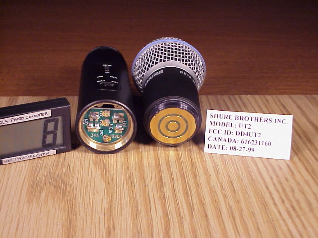
General Product Description The Shure UT2 is a low cost wireless handheld transmitter designed for the Music industry (MI) market. The UT2 is a single frequency, crystal controlled transmitter with a 9 volt battery for power supply. The frequency range for the UT2 is 596 to 608, 614 to 626, 740 to 752 and 770 to 862MHz. ISpecial Features 1.Power on/off LED to indicate the operating status of the transmitter. 2.Low profile on/off power switch prevents accidental turn-off. 3.Low battery indicator to inform the user when to change the battery. 4.Mute Switch to provide audio on /off function without turning the transmitter off. 5.A variety microphone heads may be used with the transmitter. 6. Adjustable gain provided for various source levels. 7. May be used with dynamic or condenser type microphones. 8. Electronic circuitry prevents damage to the unit if the user installs the battery reversed. 9. Compatible with SHURE UT4 receiver.
Parts List/Tune Up Info
Description:UT2 handheld transmitterDRWG. UT2-7 Refer To Drawing NOS. 90-8787G-11 Page 1 of 9 SSRecord of Changes Made 1.Production Release 2ECO 81418: Changes to audio limits pages 2 & 4 Exp Dwg. No: Used in: SHURE BROTHERS INC. 222 HARTREY AVENUE EVANSTON, IIL 60202 PHONE 847-866-2200 Microphones-Electronic Components Typed:Anny Liao, Erick Boughton Checked: Approved: Kevin Mikes Approved: Shure Model UT2 T-series UHF Handheld Transmitter Project #16996 Outline General Product Description I Special Features II Circuit Description III Test Equipment IV Alignment Procedure V Test for Product Acceptance VI Agency Approvals VII Mechanical Specification VIII Environmental Specification IX Service Evaluation General Product Description The Shure UT2 is a low cost wireless handheld transmitter designed for the Music industry (MI) market. The UT2 is a single frequency, crystal controlled transmitter with a 9 volt battery for power supply. The frequency range for the UT2 is 596 to 608, 614 to 626, 740 to 752 and 770 to 862MHz. I Special Features 1. Power on/off LED to indicate the operating status of the transmitter. 2. Low profile on/off power switch prevents accidental turn-off. 3. Low battery indicator to inform the user when to change the battery. 4. Mute Switch to provide audio on /off function without turning the transmitter off. 5. A variety microphone heads may be used with the transmitter. 6. Adjustable gain provided for various source levels. 7. May be used with dynamic or condenser type microphones. 8. Electronic circuitry prevents damage to the unit if the user installs the battery reversed. 9. Compatible with SHURE UT4 receiver. II Circuit Description Audio Section Signals Audio signals enter the UT2 through gold sliding contacts from the Microphone head to the headboard. Contact GND is a ground, Contact AUD.IN is the audio input, contact +9V supplies regulated +9 Vdc bias Description:UT2 handheld transmitterDRWG. UT2-7 Refer To Drawing NOS. 90-8787G-11 Page 2 of 9 SSRecord of Changes Made 1.Production Release 2ECO 81418: Changes to audio limits pages 2 & 4 Exp Dwg. No: Used in: SHURE BROTHERS INC. 222 HARTREY AVENUE EVANSTON, IIL 60202 PHONE 847-866-2200 Microphones-Electronic Components Typed:Anny Liao, Erick Boughton Checked: Approved: Kevin Mikes Approved: for electret condenser microphone. Preamplifier Stage Next, the audio signal enters a preamplifier stage consisting of one section of op amp (U102B). The voltage gain of this stage may be adjusted over a26dB range by means of an externally-accessible potentiometer (R125). This enables the user to compensate for level difference at the source. The output of this stage is then divided down to match the input range of the next stage via R149 and R150. Preemphasis The preamplified audio signal is then passed through a passive pre- emphasis network consisting of R142, C110, C111, R112, and R115. Audio Signal Compression The signal next enters the NE571D integrated circuit compander (U101B), providing a 2:1 logarithmic compression of the audio signal. A lower noise floor is achieved with the assistance of U102C. An internal potentiometer (R130) is provided for nulling system audio distortion. Op amp U102B operates as a 2-pole active low pass filter to restrict the bandwidth of the system to audio frequencies. The NE571D also contains and identical second channel (U101A) that is used to supply regulated, low-noise 5 Vdc bias to various audio and RF circuit points. RF section Processed Audio enters R258, an internal potentiometer adjusted for 45 kHz deviation (100 % modulation) with a0.3 dBV (2.5 dBu), 1 kHz tone at the output of the audio section. The audio is then fed to varactor diode D201, which is part of the modulated oscillator-tripler/quadrupler stage (Q201). The base-emitter circuit of Q201 operates as a crystal-controlled Colpitts oscillator in the 20 MHz region. Fundamental-mode crystal Y201 is tuned to 10 kHz below series resonance by the series combination of frequency-netting coil L201, diode D201, capacitor C205, and capacitor divider C206 and C209. Frequency Stability To ensure frequency stability with changes in battery voltage, regulated +5 Vdc bias is applied to the varactor diode and to the base of Q201. Temperature compensation is provided by C206 and C209. The collector circuit of Q201 is tuned to the third/fourth harmonic of the oscillator frequency (approximately 67/90 MHz) by means of L202, C208, and C212. C220 couples RF energy to a second tuned circuit consisting of L203, C214/213, and C215 (coupling band-pass filter), which also forms a capacitively-tapped voltage divider for matching into the base of Q202, operating as a buffer amplifier. Description:UT2 handheld transmitterDRWG. UT2-7 Refer To Drawing NOS. 90-8787G-11 Page 3 of 9 SSRecord of Changes Made 1.Production Release 2ECO 81418: Changes to audio limits pages 2 & 4 Exp Dwg. No: Used in: SHURE BROTHERS INC. 222 HARTREY AVENUE EVANSTON, IIL 60202 PHONE 847-866-2200 Microphones-Electronic Components Typed:Anny Liao, Erick Boughton Checked: Approved: Kevin Mikes Approved: Frequency Tripler and Buffer The third stage (Q203) is operated as a frequency tripler with the collector circuit tuned to the intermediate frequency (approximately 200/270 MHz) (frequency output of Q202 times three). At the collector there is a double tuned circuit that perform tuning and impedance matching into the base of Q204. Q204 operates at the same frequency as Q203. The circuit looks similar to Q203 but it is a buffer stage for additional filtering of the harmonics. The fifth stage (Q205) is the last tripler in the RF circuit tuned to the output frequency. Once again, there is a double tuned circuit providing impedance matching to the amplifier stage. Amplifier and Battery/Antenna matching The amplifier brings the signal to the desired RF power. Behind the amplifier is a Collins filter, which works as a low-pass filter and a down converter from high to low impedance. After t…
Text truncated - open the document above for the full version.
Schematics
Notes:1. All resistors are in ohms, 1 / 10 W, 1%, unless otherwise specified. 2. All capacitors have a w 50 V rating unless otherwise specified. 3. The symbol indicates a PC board ground. 4. The values for frequency-dependent components, indicated by asterisks (*), are in the table. E 1999, Shure Brothers Inc. 25A1047 (SB) TP201 Osc., Quadrupler (800 MH z) or Tripler (600 MH z) Buffer Tripler Buffer Tripler Amp End Filter Ground +9 V, 30 mA P202 +9 Vdc 1234 C205 TP202 Audio Input C2041,000 pF Gnd C2031000 pF R258 10 k Ω 13 2 C201 2.2 μ F TP216 Ground 27 pF R203 49.9 k Ω D201 312 C2021,000 pF TP204 +5 Vdc L201 13 8 7 Ground Audio Gnd Gnd +5 V, 1 mA P201 1234 GndGndAud+5 V R2024.99 k Ω AC BD I252 I250 R250100 * R252100 * R253100 * R251100 * I251 I253 N250 N252 N253 N251 EG FH I256 I254 R254100 * R256100 * R257100 * R255100 * I255 I257 N254 N258 N257 N255 R204150 k Ω R208402 Ω R206 6.81 k Ω Y201 12 3 R20520 k Ω Gnd L202 1 3 2 R207100 Ω C208 1 2 C2111,000 pF 3 C2121,000 pF + C206 47 pF C20968 pF MMBTH10L I205 C216 1,000 pF C214 L203 C215 C213 C210 0.5 pF R20920 k Ω MMBTH10L C222 C220 0.5 pF L204 C218 Gnd Gnd R213 7.5 k Ω C2191,000 pF Gnd C221 C223 L205 R21030.1 k Ω R212604 Ω C217 Gnd C225 1,000 pF R21430.1 k Ω TP207 I206 C22468 pF MMBTH10L 3 1 2 I208 R215 100 Ω Gnd C226470 pF C230470 pF L206 C227 R218 10 k Ω 0.5 pF C229 L207 C228 150 pF C23418 pF C233 470 pF C232 R21730.1 k Ω 2 1 MMBTH10L Gnd C235 I209 R220 L211 C267 C238 TP210 C242 C243 330 pF C236 L208 Gnd R219100 Ω C237470 pF C240 R221 AT41533 Gnd R222 3 2 1 I211 R224 C244 150 pF C270 .0015 μ F C249 152-04 2 1 + C247 0.5 pF C250 C251 150 pF R226 L210 2 1 + C245 R223100 Ω C246150 pF Gnd C248330 pF C271 C252 1000 pF 1 2 C253 LF212162A12 C272 L213 C255 R225 C256 3 1 2 AT41533 R22733.2 Ω I212 C2574.7 pF Gnd C254 L214 15 nH 1 C25927 pF 8 In Out 4 Gnd Gnd GndGnd Gnd Gnd BPF Gnd 2 3 5 6 7 F201 3 1 2 TP217 RF Output behind the Filter C265 27 pF L218 6.8 nH J202 56A317 J201 56A318 Antenna Battery C266 27 pF L209 3 R211 100 Ω ICT Test Points I205: Stage 1 I206: Stage 2 I208: Stage 3 I209: Stage 4 I211: Stage 5 I212: Stage 6 Functional Test PointsTP201: +9 Vdc TP202: audio input TP204: +5 Vdc TP216: ground TP217: RF output for automatic test C208C218 pF Frequency-Dependent Parts 162B27 3.3 15 12 800–820 MHz E 162A27 3.3 15 12 614–626 MHz B 162A27 3.3 15 12 596–608 MHz A Group Frequency Range L210 nH C214 pF F201 Part No. 854–862 MHz H 150 10001000 C217 pF C227 pF 8.28.2 10 C232 pF 121818 150 not usednot used C235 pF 2.23.33.3 C255 pF L202L204 nH 220390390 L203L205 nH 220390390 L206L208 nH 335656 L207L209 nH 335656 L213 nH 588 301301301 R220 Ω Group Indicators * * * * Q201 * * * * * * Q202 Q203 R216402 Ω * * * * * * * * * * * * * Q204 * * Q205 * * * Q206 * * * * * * * * * * * * UT 2 RF Board (from 90_8787K-11) 10 15 150 6868 C215 pF 100 47 151515 C223 pF 15 0.50.50.5 C220 pF 1 not usednot used C222 pF not used 150 6868 C224 pF 150 3.3 4.7 C234 pF 15151822 150 C236 pF 8.28.28.23.3 1 0.50.5 C238 pF 1 not usednot usednot used C240 pF 470 C242 pF 15151818 152A04 152C04152C04 C245 Part No. 152A04 C250 pF 151212 8.2 C254 pF 18 .01 μ F .01 μ F 1500 1.5 C256 pF 3.9 1010 3.3 C267 pF 15181810 100 not usednot used C272 pF 1500 162B27 220 180 56 47 5 3.3 150 10 27.427.4 R221 k Ω 2 30.130.130.1 R222 k Ω 3.92 100301301 R224 Ω 301 2.492.212.21 R225 k Ω 2.21 4.996.816.81 R226 k Ω 6.81 49.933.233.2 R227 Ω 22.1 CarrierFrequency C253 pF not used .01 μ F .01 μ F not used 1.5 not usednot usednot used C213 pF 1.5 not usednot usednot used C249 pF not used C257 pF 4.76.88.24.7 not usednot usednot used C270 pF 1500 C273– C276 pF not usednot usednot usednot used C277 pF 6.85.65.63.3 L211 nH 2.5 885 12 1515 L214 nH 12 402402402 R216 Ω 200 * * C273 * C274 * R259 0 Ω 152-04 * C276 C277 * C275 * * 1000 not usednot used C272 pF 1500 *
Schematics
Notes:1. All resistors are 1 / 16 W, 1%, 0603 unless otherwise specified. 2. Unless otherwise specified, all capacitors have a w 50 V rating, and all non-polarized capacitors have a 10% tolerance. 3. The symbol indicates a PC board ground. E 1999, Shure Brothers Inc. 25A1047 (SB) +9 V Audio C103 1 μ F 16 V R10324.9 k Ω U102B + I102 C133 100 pF R105 24.9 k Ω I122 R1060 Ω R148 24.9 k Ω I119 I105 C105 1 μ F Audio In I111 R110 499 Ω C134 100 pF R10824.9 k Ω C131 33 pF C11333 pF 5 6 +− I114 R147 0 Ω 7 I124 I123 2 31 R125100 k Ω Log CW 188A49 R1192.49 k Ω I120 C12010 μ F +9 V Audio +9 V +9 V R1161k Ω + + C1164.7 μ F 16 V 1234 Audio to RF P101 +5 V to RF +9 V to RF P102 1234 Shield I133 +9 V to RF C1264.7 μ F 16 V I138 S101 2 1 3 +9 V Audio Q105 183A07 3 2 1 L101 + 162A03 C127150 pF 55A8087 +9 V I+9 I148 D103184D18Green I156 Q110 183A38 1 2 3 I157 1 3 2 Q109 183A38 R1466.81 k Ω JP106 I100 2 183A38 Q107 3 1 I150 D102 184B18Yellow I150 I153 R145 60.4 k Ω 0 Ω R1324.02 k Ω JP105 0 Ω R1314.02 k Ω I139 I137 R1443.01 k Ω I141 D101 184A18Red I131 R134 18.2 k Ω I142 R1396.81 k Ω C132 150 pFQ108 183A38 2 3 1 Q106 183A38 2 3 1 I152 R1384.99 k Ω I149 R13645.3 k Ω R143 20 k Ω I136 L102 1.8 μ H J101 56A317 I140 J10256A318 L103 I145 2k Ω R142 I155 C110 0.33 μ F I116 R112 100 k Ω I112 C111 3300 pF R115 2k Ω I115 R11724.9 k Ω I103 + C1061 μ F 16 V Pin 9 of U101 R101 10 k Ω R10724.9 k Ω C10147 μ F 10 V + I101 C10247 μ F 10 V R102 4.99 k Ω +− 1213 14 I107 U102C 188A49 C13627 pF U101B 188A01 12 + C1094.7 μ F 16 V I125 14 I121 1011 – + G 15 .0068 μ F I128 R124, 40.2 k Ω + C1171 μ F 16 V 16 9 C121 I151 R126 60.4 k Ω I130 R14075 k Ω +5 V C124150 pF R129 I134 2 10 k Ω R13020 k Ω 1 I154 3 10 k Ω R141 + C125 1 μ F 16 V Distortion C1084.7 μ F 16 V + I113 10 k Ω R113 I118 I117 R114 12.1 k Ω 10 9 +− R109 402 k Ω + I106 +5 V R104100 k Ω C104 1 μ F, 16 V U102D 188A49 8 I110 R118 10 k Ω 330 pF C112 + I108 R111249 Ω C107 4.7 μ F, 16 V I109 Audio to RF JP107 0 Ω C123 1 μ F 16 V + I135 S102 55A8087 1 2 3 AGnd C1152200 pF +5 V + C1194.7 μ F 16 V I127 23 I129 R123 1k Ω 1 Q104 183A01 2.49 k Ω R128 R127 2.49 k Ω I132 1 R122 2 1k Ω I126 N126 + C118 4.7 μ F 16 V 3 Q103 183A01 +5 V R135 49.9 k Ω I144 U101A 188A01 +− 18 2 G 37 I143 6 R133 13.3 k Ω I+5 AGnd R137 100 Ω I146 L104 162A03 I147 C128150 pF +5 V to RF +5 V +9 V Audio +9 V Audio +9 V +9 V C129150 pF U101C 188A01 13 4 4 U102E 188A49 11 V+V– C1300.1 μ F 32 U102A 188A49 +– 1 Not used I104 1.8 μ H + UT 2 Audio Board (from 90_8787K-11) C13547 pF Gain R150750 Ω 604 Ω R149 Mute Power
Schematics
Notes:1. All resistors are 1 / 16 W, 1%, 0603 unless otherwise specified. 2. Unless otherwise specified, all capacitors have a w 50 V rating, and all non-polarized capacitors have a 10% tolerance. 3. The symbol indicates a PC board ground. E 1999, Shure Brothers Inc. 25A1047 (SB) +9 V Audio C103 1 μ F 16 V R10324.9 k Ω U102B + I102 C133 100 pF R105 24.9 k Ω I122 R1060 Ω R148 24.9 k Ω I119 I105 C105 1 μ F Audio In I111 R110 499 Ω C134 100 pF R10824.9 k Ω C131 33 pF C11333 pF 5 6 +− I114 R147 0 Ω 7 I124 I123 2 31 R125100 k Ω Log CW 188A49 R1192.49 k Ω I120 C12010 μ F +9 V Audio +9 V +9 V R1161k Ω + + C1164.7 μ F 16 V 1234 Audio to RF P101 +5 V to RF +9 V to RF P102 1234 Shield I133 +9 V to RF C1264.7 μ F 16 V I138 S101 2 1 3 +9 V Audio Q105 183A07 3 2 1 L101 + 162A03 C127150 pF 55A8087 +9 V I+9 I148 D103184D18Green I156 Q110 183A38 1 2 3 I157 1 3 2 Q109 183A38 R1466.81 k Ω JP106 I100 2 183A38 Q107 3 1 I150 D102 184B18Yellow I150 I153 R145 60.4 k Ω 0 Ω R1324.02 k Ω JP105 0 Ω R1314.02 k Ω I139 I137 R1443.01 k Ω I141 D101 184A18Red I131 R134 18.2 k Ω I142 R1396.81 k Ω C132 150 pFQ108 183A38 2 3 1 Q106 183A38 2 3 1 I152 R1384.99 k Ω I149 R13645.3 k Ω R143 20 k Ω I136 L102 1.8 μ H J101 56A317 I140 J10256A318 L103 I145 2k Ω R142 I155 C110 0.33 μ F I116 R112 100 k Ω I112 C111 3300 pF R115 2k Ω I115 R11724.9 k Ω I103 + C1061 μ F 16 V Pin 9 of U101 R101 10 k Ω R10724.9 k Ω C10147 μ F 10 V + I101 C10247 μ F 10 V R102 4.99 k Ω +− 1213 14 I107 U102C 188A49 C13627 pF U101B 188A01 12 + C1094.7 μ F 16 V I125 14 I121 1011 – + G 15 .0068 μ F I128 R124, 40.2 k Ω + C1171 μ F 16 V 16 9 C121 I151 R126 60.4 k Ω I130 R14075 k Ω +5 V C124150 pF R129 I134 2 10 k Ω R13020 k Ω 1 I154 3 10 k Ω R141 + C125 1 μ F 16 V Distortion C1084.7 μ F 16 V + I113 10 k Ω R113 I118 I117 R114 12.1 k Ω 10 9 +− R109 402 k Ω + I106 +5 V R104100 k Ω C104 1 μ F, 16 V U102D 188A49 8 I110 R118 10 k Ω 330 pF C112 + I108 R111249 Ω C107 4.7 μ F, 16 V I109 Audio to RF JP107 0 Ω C123 1 μ F 16 V + I135 S102 55A8087 1 2 3 AGnd C1152200 pF +5 V + C1194.7 μ F 16 V I127 23 I129 R123 1k Ω 1 Q104 183A01 2.49 k Ω R128 R127 2.49 k Ω I132 1 R122 2 1k Ω I126 N126 + C118 4.7 μ F 16 V 3 Q103 183A01 +5 V R135 49.9 k Ω I144 U101A 188A01 +− 18 2 G 37 I143 6 R133 13.3 k Ω I+5 AGnd R137 100 Ω I146 L104 162A03 I147 C128150 pF +5 V to RF +5 V +9 V Audio +9 V Audio +9 V +9 V C129150 pF U101C 188A01 13 4 4 U102E 188A49 11 V+V– C1300.1 μ F 32 U102A 188A49 +– 1 Not used I104 1.8 μ H + UT 2 Audio Board (from 90_8787K-11) C13547 pF Gain R150750 Ω 604 Ω R149 Mute Power
Schematics
Notes:1. All resistors are in ohms, 1 / 10 W, 1%, unless otherwise specified. 2. All capacitors have a w 50 V rating unless otherwise specified. 3. The symbol indicates a PC board ground. 4. The values for frequency-dependent components, indicated by asterisks (*), are in the table. E 1999, Shure Brothers Inc. 25A1047 (SB) TP201 Osc., Quadrupler (800 MH z) or Tripler (600 MH z) Buffer Tripler Buffer Tripler Amp End Filter Ground +9 V, 30 mA P202 +9 Vdc 1234 C205 TP202 Audio Input C2041,000 pF Gnd C2031000 pF R258 10 k Ω 13 2 C201 2.2 μ F TP216 Ground 27 pF R203 49.9 k Ω D201 312 C2021,000 pF TP204 +5 Vdc L201 13 8 7 Ground Audio Gnd Gnd +5 V, 1 mA P201 1234 GndGndAud+5 V R2024.99 k Ω AC BD I252 I250 R250100 * R252100 * R253100 * R251100 * I251 I253 N250 N252 N253 N251 EG FH I256 I254 R254100 * R256100 * R257100 * R255100 * I255 I257 N254 N258 N257 N255 R204150 k Ω R208402 Ω R206 6.81 k Ω Y201 12 3 R20520 k Ω Gnd L202 1 3 2 R207100 Ω C208 1 2 C2111,000 pF 3 C2121,000 pF + C206 47 pF C20968 pF MMBTH10L I205 C216 1,000 pF C214 L203 C215 C213 C210 0.5 pF R20920 k Ω MMBTH10L C222 C220 0.5 pF L204 C218 Gnd Gnd R213 7.5 k Ω C2191,000 pF Gnd C221 C223 L205 R21030.1 k Ω R212604 Ω C217 Gnd C225 1,000 pF R21430.1 k Ω TP207 I206 C22468 pF MMBTH10L 3 1 2 I208 R215 100 Ω Gnd C226470 pF C230470 pF L206 C227 R218 10 k Ω 0.5 pF C229 L207 C228 150 pF C23418 pF C233 470 pF C232 R21730.1 k Ω 2 1 MMBTH10L Gnd C235 I209 R220 L211 C267 C238 TP210 C242 C243 330 pF C236 L208 Gnd R219100 Ω C237470 pF C240 R221 AT41533 Gnd R222 3 2 1 I211 R224 C244 150 pF C270 .0015 μ F C249 152-04 2 1 + C247 0.5 pF C250 C251 150 pF R226 L210 2 1 + C245 R223100 Ω C246150 pF Gnd C248330 pF C271 C252 1000 pF 1 2 C253 LF212162A12 C272 L213 C255 R225 C256 3 1 2 AT41533 R22733.2 Ω I212 C2574.7 pF Gnd C254 L214 15 nH 1 C25927 pF 8 In Out 4 Gnd Gnd GndGnd Gnd Gnd BPF Gnd 2 3 5 6 7 F201 3 1 2 TP217 RF Output behind the Filter C265 27 pF L218 6.8 nH J202 56A317 J201 56A318 Antenna Battery C266 27 pF L209 3 R211 100 Ω ICT Test Points I205: Stage 1 I206: Stage 2 I208: Stage 3 I209: Stage 4 I211: Stage 5 I212: Stage 6 Functional Test PointsTP201: +9 Vdc TP202: audio input TP204: +5 Vdc TP216: ground TP217: RF output for automatic test C208C218 pF Frequency-Dependent Parts 162B27 3.3 15 12 800–820 MHz E 162A27 3.3 15 12 614–626 MHz B 162A27 3.3 15 12 596–608 MHz A Group Frequency Range L210 nH C214 pF F201 Part No. 854–862 MHz H 150 10001000 C217 pF C227 pF 8.28.2 10 C232 pF 121818 150 not usednot used C235 pF 2.23.33.3 C255 pF L202L204 nH 220390390 L203L205 nH 220390390 L206L208 nH 335656 L207L209 nH 335656 L213 nH 588 301301301 R220 Ω Group Indicators * * * * Q201 * * * * * * Q202 Q203 R216402 Ω * * * * * * * * * * * * * Q204 * * Q205 * * * Q206 * * * * * * * * * * * * UT 2 RF Board (from 90_8787K-11) 10 15 150 6868 C215 pF 100 47 151515 C223 pF 15 0.50.50.5 C220 pF 1 not usednot used C222 pF not used 150 6868 C224 pF 150 3.3 4.7 C234 pF 15151822 150 C236 pF 8.28.28.23.3 1 0.50.5 C238 pF 1 not usednot usednot used C240 pF 470 C242 pF 15151818 152A04 152C04152C04 C245 Part No. 152A04 C250 pF 151212 8.2 C254 pF 18 .01 μ F .01 μ F 1500 1.5 C256 pF 3.9 1010 3.3 C267 pF 15181810 100 not usednot used C272 pF 1500 162B27 220 180 56 47 5 3.3 150 10 27.427.4 R221 k Ω 2 30.130.130.1 R222 k Ω 3.92 100301301 R224 Ω 301 2.492.212.21 R225 k Ω 2.21 4.996.816.81 R226 k Ω 6.81 49.933.233.2 R227 Ω 22.1 CarrierFrequency C253 pF not used .01 μ F .01 μ F not used 1.5 not usednot usednot used C213 pF 1.5 not usednot usednot used C249 pF not used C257 pF 4.76.88.24.7 not usednot usednot used C270 pF 1500 C273– C276 pF not usednot usednot usednot used C277 pF 6.85.65.63.3 L211 nH 2.5 885 12 1515 L214 nH 12 402402402 R216 Ω 200 * * C273 * C274 * R259 0 Ω 152-04 * C276 C277 * C275 * * 1000 not usednot used C272 pF 1500 *
Test Report
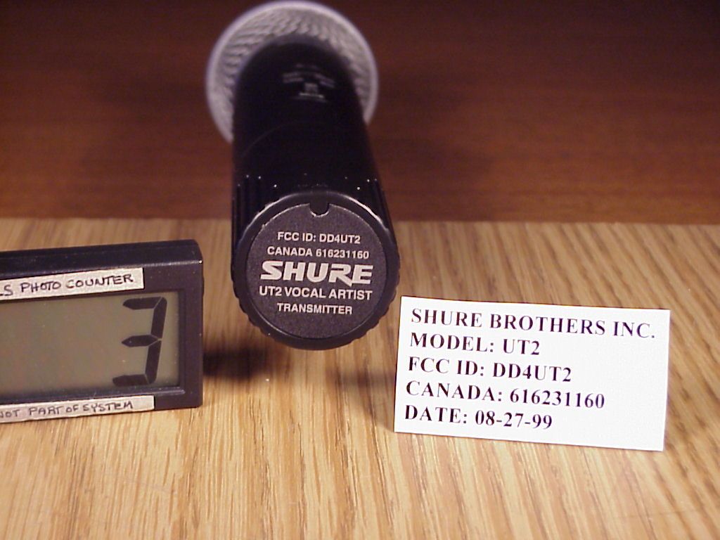
EMC Test ServicesReport No. 7584 1250 Peterson Drive, Wheeling, Illinois 60090, USA09/22/99 Page 1 TEST SPECIFICATION: FCC "Rules and Regulations", Part 74, Experimental Radio, Auxiliary, Special Broadcast and Other Program Distribution Services for Operation in the 614 to 806 MHz Band Subpart H, Low Power Auxiliary Stations Sections 74.801 to 74.882 THE FOLLOWING MEETS THE ABOVE TEST SPECIFICATION Formal Name:Shure UT2 Vocal Artist Transmitter Kind of Equipment:Handheld wireless microphone transmitter Test Configuration:Single Channel Crystal Controlled Emission Designator:120KF3E Transmitter FCC ID:DD4UT2 Model Number: UT2 Serial Number: NA Dates of Test:August 16, 20 & 25, 1999 Test Conducted For:Shure, Inc. 222 Hartrey Avenue Evanston, Illinois 60202-3696 NOTICE:Please see change information listed inside of this report. This report must not be used by the customer to claim product endorsement by NVLAP or any agency of the United States Government, and it cannot be reproduced (except in full), without the approval of D.L.S. Electronic Systems Inc. EMC Test ServicesReport No. 7584 1250 Peterson Drive, Wheeling, Illinois 60090, USA09/22/99 Page 2 SIGNATURE PAGE Report Written By: Arnom C. Rowe Test Engineer EMC-001375-NE Report Reviewed by: Jack Prawica Lab Manager Report Approved by: Brian J. Mattson General Manager Company Official: Shure, Inc. Page 3 Page 4 EMC Test ServicesReport No. 7584 1250 Peterson Drive, Wheeling, Illinois 60090, USA09/22/99 Page 5 1.Cover Pagei 2.Signature Pageii 3.NBS Certificate of Accreditationiii 5.Table of Contentsiv 7.Summary of Test Report1.0 7.Introduction2.0 7.Object3.0 7.Test Set-up4.0 8.Test Equipment (Bandwidths and Detector Function)5.0 8.RF Power Output6.0 9.Graphs taken of the RF Power Output Measurements6.0 14.Modulation Characteristics7.0 15.Graphs taken of the Modulation Characteristics7.0 18.Occupied Bandwidth8.0 19.Graphs taken of the Occupied Bandwidth8.0 20.Frequency Deviation9.0 21.Graphs taken of the Frequency Deviation9.0 22.Spurious Emission Measurements at Antenna Terminals10.0 23.Conducted Emission Data taken10.0 24.Conducted Emission Graphs Taken10.0 EMC Test ServicesReport No. 7584 1250 Peterson Drive, Wheeling, Illinois 60090, USA09/22/99 Page 6 25.Field Strength of Spurious Emission Measurements11.0 27.Radiated Data taken for Field Strength Measurements11.0 32.Radiated Graphs taken for Field Strength Measurements11.0 49.Frequency Stability (Temperature)12.0 50.Graphs taken of Frequency Stability (Temperature)12.0 61.Frequency Stability (Voltage Variation)13.0 62.Photo Information and Test Set-Up14.0 63.Photos Taken During Testing15.0 69.Change Information16.0 71.Results of Tests17.0 71.Conclusion18.0 72.Equipment ListTABLE 1 EMC Test ServicesReport No. 7584 1250 Peterson Drive, Wheeling, Illinois 60090, USA09/22/99 Page 7 1.0SUMMARY OF TEST REPORT It was found that the Shure UT2 Vocal Artist Transmitter S/N NA meets the radio interference emission requirements of the FCC "Rules and Regulations", Part 74, Subpart H, Sections 74.801 to 74.882 for Low Power Auxiliary Stations operating in the 740 to 752 MHz Frequency Band. 2.0INTRODUCTION On August 16, 20 & 25, 1999, a series of radio frequency interference measurements were performed on Handheld wireless microphone transmitter, S/N NA. The tests were performed according to the procedures of FCC as stated in Part 2 Subpart J, Equipment Authorization …
Text truncated - open the document above for the full version.
Contact Information
Applicant
Craig Kozokar(EMC Project Engineer)
Technical Contact
SHURE INCEDGAR C REIHL
[email protected](847) 866-2289
222 HARTREY AVE · EVANSTON, Illinois · United States
Non-Technical Contact
SHURE INC.ALBERT J WAHOUT
[email protected](847) 866-2654
Test Firm
DLS Electronic Systems, Inc.William Stumpf
Technical Specifications
| # | Rule Parts | Frequency Range | Power Output | Emission | Tolerance |
|---|---|---|---|---|---|
| 1 | 74H | 740 MHz - 752 MHz | 4.17 mW | 120KF3E | 0.0050000000 % |
Other Applications from Shure Incorporated
DD4IMXBP
Dec 24, 2025UC Wall
Equipment Class
NII - Unlicensed National Information Infrastructure TXDD4SLXD3EG57
Jul 25, 2025Plug-on Wireless Transmitter
Equipment Class
DTS - Digital Transmission System
DD4ULXD8G50
Sep 18, 2024Wireless Gooseneck Transmitter
Equipment Class
DWM - Part 15 Wireless Microphone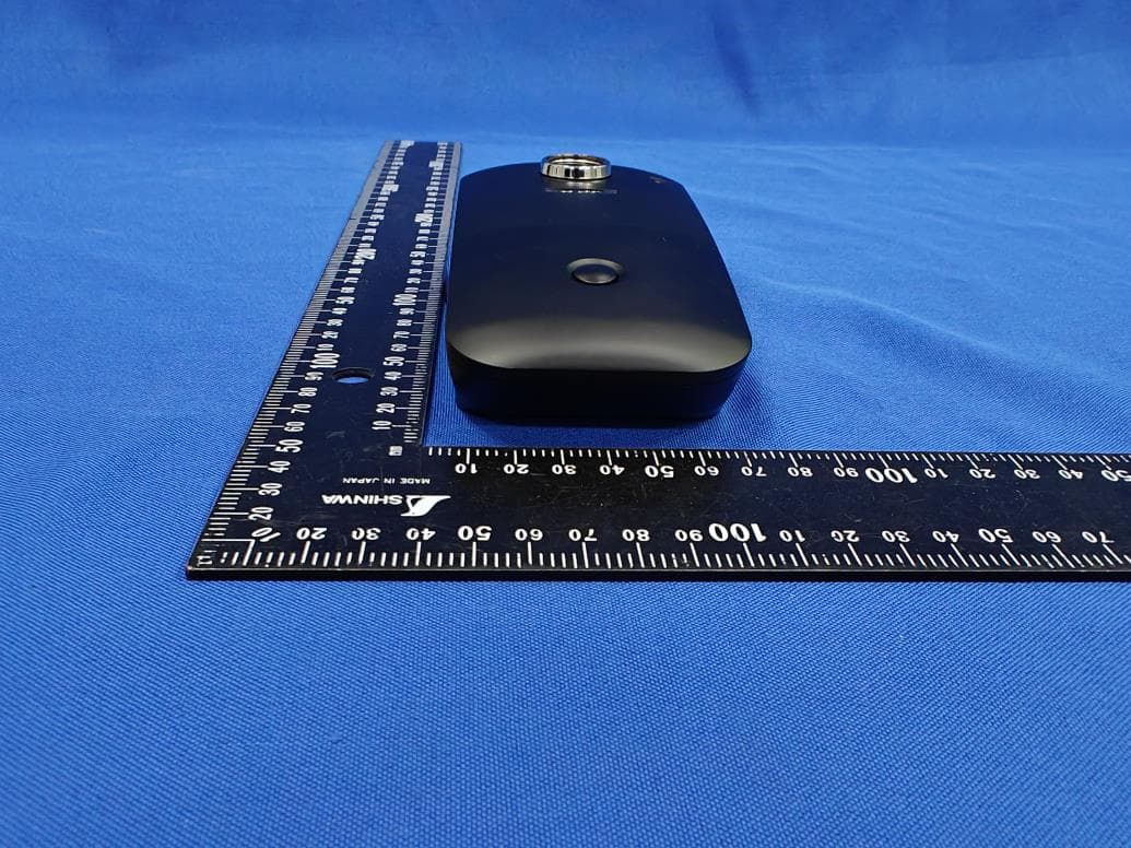
DD4ULXD8H50
Sep 18, 2024Wireless Gooseneck Transmitter
Equipment Class
DWM - Part 15 Wireless Microphone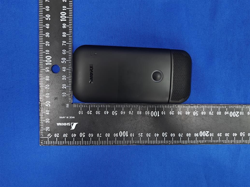
DD4ULXD6G50
Sep 08, 2024Wireless Boundary Transmitter
Equipment Class
TLD - Licensed LPAS Device