E5M-EL-705EL705
GE MDS, LLC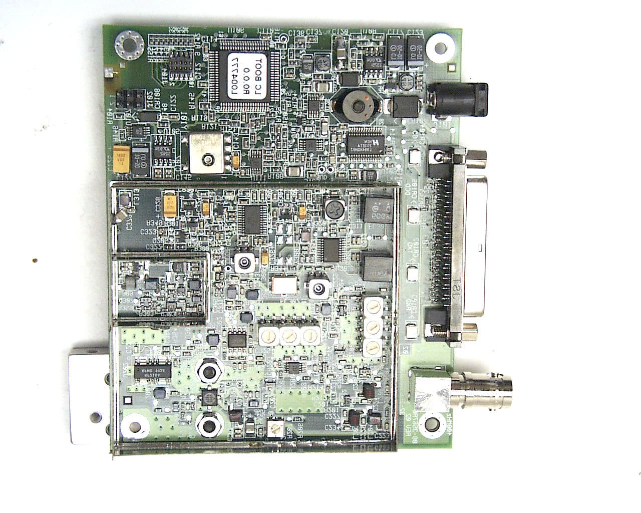
Click to zoom
Application Details
- Equipment Class
- TNB - Licensed Non-Broadcast Station Transmitter
- Date of Grant
- Aug 27, 2000
- Application Purpose
- Original Equipment
- Date of Application
- Jul 24, 2000
- Equipment Note
- EL705
- Frequency Range
- 450.00000000 - 470.00000000
- Company
- GE MDS, LLC
- Country
- United States
Documents & Files
Document Text
Text extracted from the exhibit documents filed with the FCC. Open a document above to read the original.
Users Manual
MDS 05-3624A01, Rev. A JUNE 2000 Data Transceiver MDS OEM-L/ss QUICK START GUIDE Below are the basic steps for installing the transceiver. Detailed instructions are given in “Installation Steps” on page 8 of this guide. 1. Install and connect the antenna system to the radio • Use good quality, low loss coaxial cable. Keep the feedline as short as possible. • Preset directional antennas in the direction of desired transmission. 2. Connect the data equipment to the radio’s INTERFACE connector • Connection to the radio must be made with a DB-25 Male connector. Connections for typical sys- tems are shown below. • Connect only the required pins. Do not use a straight-through RS-232 cable with all pins wired. • Verify the data equipment is configured as DTE. (By default, the radio is configured as DCE.) The markup had a question about this figure. Please verify 3. Apply DC power to the radio (10–30 Vdc @ 1.5 A minimum) • Observe proper polarity. 4. Set the radio’s basic configuration with a Hand-Held Terminal (HHT) • Set the transmit frequency ( TX xxx.xxx ). • Set the receive frequency ( RX xxx.xxx ). • Set the network address ( ADDR xxx ). • Set/verify the data rate using the BAUD command. The default setting is BAUD 9600 8N1 . (Refer to “TRANSCEIVER PROGRAMMING” on page 14 for command details.) 5. Verify proper operation by observing the LED display • Refer to Table 5 on page 14 for a description of the status LEDs. • Refine directional antenna headings for maximum receive signal strength using the RSSI command. DB-25DB-25 TRANSCEIVER (DCE) 2 3 2 3 RTU (DTE) 4 5 20 6DSR DSR 6 RXD TXD GND RTS CTS TXD RXD GND 4 CTS 5 RTS DB-9DB-25 DB-9 to DB-25 ExampleDB-25 to DB-25 Example 11 4 5 TRANSCEIVER (DCE) 2 3 2 3 RTU (DTE) 5 20 7 RXD TXD DCD GND DSR RTS TXD RXD DCD GND As required for application 5 18 7 6 CTS DSR RTS CTS8 6 4 5 77 GND GND 88 DCD DCD As required for application MDS 05-3624A01, Rev. AInstallation and Operation Guidei TABLE OF CONTENTS 1.0 GENERAL.................................................................................... 1 1.1 Introduction ...................................................................................... 1 1.2 Differences Among Models .............................................................. 1 1.3 Applications ...................................................................................... 2 Point-to-Multipoint, Multiple Address Systems (MAS) .................... 2 Point-to-Point System ..................................................................... 3 Switched Carrier Operation ............................................................ 4 Single Frequency (Simplex) Operation ........................................... 4 1.4 Model Number Codes ...................................................................... 4 1.5 Accessories ...................................................................................... 5 2.0 GLOSSARY OF TERMS.............................................................. 5 3.0 INSTALLATION ............................................................................ 8 3.1 Installation Steps .............................................................................. 8 3.2 Mounting the Transceiver Board ....................................................... 9 3.3 Mounting the Enclosed Transceiver ............................................... 10 3.4 Antennas and Feedlines ................................................................ 10 Feedlines ...................................................................................... 11 3.5 Power Connection .......................................................................... 11 3.6 Data Interface Connections ............................................................ 12 3.7 Power Conservation ....................................................................... 12 4.0 OPERATION .............................................................................. 13 4.1 LED Indicators ................................................................................ 14 5.0 TRANSCEIVER PROGRAMMING ............................................ 14 5.1 Hand-Held Terminal Connection & Startup .................................... 15 5.2 Hand-Held Terminal Setup ............................................................. 16 5.3 Keyboard Commands ..................................................................... 17 Entering Commands ..................................................................... 17 Error Messages ............................................................................ 17 5.4 Detailed Command Descriptions ................................................... 19 ADDR [0–255] .............................................................................. 19 AMASK [0000 0000–FFFF FFFF] ................................................ 19 BAUD [xxxxx abc] ......................................................................... 20 CTS [0–255] ................................................................................. 20 CTSHOLD [0–60000] ................................................................... 21 DEVICE [DCE | CTS KEY] ........................................................... 21 DKEY ............................................................................................ 21 INIT ............................................................................................... 22 KEY .............................................................................................. 22 iiInstallation and Operation GuideMDS 05-3624A01, Rev. A OWM [XXX...] ............................................................................... 22 OWN [XXX...]................................................................................ 22 PWR [L | M | H] ............................................................................. 23 RSSI and RSSI! ............................................................................ 23 RX [xxx.xxx] .…
Text truncated - open the document above for the full version.
Cover Letter(s)
June 26, 2000 FEDERAL COMMUNICATIONS COMMISSION 7435 Oakland Mills Road Columbia, MD 21046 USA Subject:Type Acceptance Application under FCC CFR 47, Parts 2 and 90 (Subpart I) - Radio Services Transmitters Operating in the frequency band 450-470 MHz (12.5 kHz Channel Spacing). Applicant:ADAPTIVE BROADBAND Product:EL705 DATA TRANSCEIVER Model:EL7054F0D0ANN1N FCC ID:E5M-EL-705 Dear Sir/Madam, As appointed agent for ADAPTIVE BROADBAND, we would like to submit the application for certificate of the above product. All technical and administrative documents have been uploaded to FCC OET electronic filing system as required. If you have any queries, please do not hesitate to contact us by our TOLL FREE numbers: OUR TELEPHONE NO.:1-877-765-4173 Yours truly, Tri Minh Luu, P. Eng., V.P., Engineering TML/AK Encl. 2 3000 Bristol Circle, Oakville, Ontario, Canada L6H 6G4 Telephone (905) 829-1570 Facsimile (905) 829-8050 Website: www.ultratech-labs.com Email: [email protected] UltraTech Group of Labs
Cover Letter(s)
Ladies/Gentlemen, Please allow us to correct the Emission Designation stated in the Form 731 and page 7 of our test report # MIC28-F90. The calculation of the necessary bandwidth is incorrect since we applied the incorrect level of FM modulation. The correct level of FM modulation shall be 4, not 2 as we used for original calculation, below please find our recalculation: For Channel Spacing = 12.5 kHz, D = 2.5 kHz max, K=1, M = Max. Data Rate inkb/s / Level of FM = 9.6/4 = 2.4 Level of FM = 4 Bn = 2M + 2DK – 2*2.4 + 2+2.5*1 = 9.8 kHz Our measurements per plots # 1 to 3 in Exhibit 9 of the test report show the 99% BW of 9.2 kHz maximum which agrees with calculation. The Emission Designation is 9K8F1D Please allow us to correct the emission designation as above in our application. Please contact us if if you have any questions. Regards, Tri M. Luu, P.Eng Authorized Agent Ultratech Engineering Labs Inc. FAX MESSAGE 3000 Bristol Circle Oakville, Ontario. L6H-6G4 DATE:08/04/00 TO:F.C.C. ATTN:To Whom It may Concern SUBJECT:FCC ID: E5M-EL-705, 731 Confirmation No.: EA98272 PAGE 1 OF 1 FROM:Tri Luu Email Address: [email protected] PHONE:(905)-829-1570 FAX:(905)-829-8050
External Photos
EXHIBIT 11 - PHOTOGRAPHS OF EUT PHOTO #1 OF 6 EXHIBIT 11 - PHOTOGRAPHS OF EUT PHOTO #2 OF 6 EXHIBIT 11 - PHOTOGRAPHS OF EUT PHOTO #3 OF 6 EXHIBIT 11 - PHOTOGRAPHS OF EUT PHOTO #4 OF 6 EXHIBIT 11 - PHOTOGRAPHS OF EUT PHOTO #5 OF 6 EXHIBIT 11 - PHOTOGRAPHS OF EUT PHOTO #6 OF 6
ID Label/Location Info
EXHIBIT 15 - FCC ID LABEL FCC ID: E5M-EL-705 This device complies with Part 15 of the FCC Rules. Operation is subject to the following two conditions: (1) this device may not cause harmful interference and (2) this device must accept any interference received, including interference that may cause undesired operation
ID Label/Location Info
June 26, 2000 FEDERAL COMMUNICATIONS COMMISSION 7435 Oakland Mills Road Columbia, MD 21046 USA Subject:Type Acceptance Application under FCC CFR 47, Parts 2 and 90 (Subpart I) - Radio Services Transmitters Operating in the frequency band 450-470 MHz (12.5 kHz Channel Spacing). Applicant:ADAPTIVE BROADBAND Product:EL705 DATA TRANSCEIVER Model:EL7054F0D0ANN1N FCC ID:E5M-EL-705 Dear Sir/Madam, As appointed agent for ADAPTIVE BROADBAND, we would like to submit the application for certificate of the above product. All technical and administrative documents have been uploaded to FCC OET electronic filing system as required. If you have any queries, please do not hesitate to contact us by our TOLL FREE numbers: OUR TELEPHONE NO.:1-877-765-4173 Yours truly, Tri Minh Luu, P. Eng., V.P., Engineering TML/AK Encl. 2 3000 Bristol Circle, Oakville, Ontario, Canada L6H 6G4 Telephone (905) 829-1570 Facsimile (905) 829-8050 Website: www.ultratech-labs.com Email: [email protected] UltraTech Group of Labs
Operational Description
2.0 Description of Device Operation 2.1 General Operation The EL-705 Data Transceiver is an OEM narrow band radio designed to operate on 12.5kHz channels, meeting the requirements of FCC Part 90 and FCC Part 15. 2.2 Summary of RF Parameters Transmitter Type: Synthesized, 12.5kHz steps. Frequency Range: 450 to 470MHz. Power Output: +33dBm, nominal. Master Clock Reference: 16MHz TCXO, +/- 1.5ppm stability. Receiver Type: Double conversion superheterodyne. Frequency Range: 450 to 470MHz. 1 st IF Frequency: 45MHz 1 st LO Range: Low-side injection 405 to 425MHz, 12.5kHz steps. 2 nd IF Frequency: 450kHz. 2 nd LO Frequency: Low-side injection 44.550MHz, fixed. 2.3 Description of Circuit Functions The following is a summary of the operation of the EL-705 Data Transceiver, and is referenced to the block diagram shown in Figure 1. 2.3.1 Receiver Receiver Front End RF for both transmit and receive is connected to the OEM transceiver board thru the BCN antenna connector J201. In the receive mode, the received signals first pass thru a 5 th order lumped-element harmonic lowpass filter. This filter suppresses all signal energy above the receive band of interest. Following this lowpass filter, the received signals are passed thru an antenna switch which is in the off mode in receive and directs the signal energy to a 3-section helical bandpass filter, FL200. The output of FL200 is then passed thru a low-noise RF preamplifier, Q201, and then thru another 3-section helical bandpass filter, FL201. The combination of both 3-section helical filters has approximately a 20MHz bandwidth, suitable to cover the 450 to 470MHz band and provide sufficient rejection of the undesired out of band signals. The filtered and amplified received signals are then passed thru to a double-balanced IC mixer, U301 that, in conjunction with the 1 st local oscillator signal, downconvert the desired signal to the 1 st IF of 45MHz. The 1 st conversion process to 45MHz utilizes a low-side injection method. Since the receive range is 450 to 470MHz in 12.5kHz steps, the 1 st LO will cover 405 to 425MHz in 12.5kHz steps. 1 st Intermediate Frequency The 1 st IF is filtered by a 3-pole monolithic crystal filter, FL302. This filter has a center frequency of 45MHz and has a bandwidth of 15kHz. Since the first mixer has gain, no IF amplifier is needed. Hence the filtered output of the 1 st IF is fed directly to the SA-606 FM demodulator IC for further processing. 1 st Local Oscillator The first conversion process mixes the filtered and pre-amplified received signal with a locally generated signal source that is phase locked to a 16MHz master TCXO crystal. This 1 st local oscillator is generated from a VCO circuit consisting of Q303 and Q307 and its associated components. The VCO output signal is buffered by U302, and a portion of this signal is fed back to the PLL synthesizer IC, U300, which divides it down using a set of on-chip programmable dividers and compares the result to a divided-down version of the 16MHz master clock in a phase detector. Any static or rotating phase difference between the two signals generates a series of current pulses at a rate of 50 kHz which are converted to a steering voltage in the loop filter. This filtered voltage is then used in concert with a variable-capacitance diode in the VCO circuit to correct this offset to zero. The loop filter also serves to control loop dynamics, suppress the 50kHz phase detector sampling frequency, and noise. The programmable feedback divider string within U300 can also divide the VCO by a fractional part, so smaller than 50kHz increments can be had; thus, 12.5kHz steps can be generated. The other VCO output is split into two paths. One path is filtered by a single-section elliptic lowpass filter to reduce the harmonic content, and the result serves as the 1 st local oscillator signal in the 1 st conversion process already described. The second signal path is fed to the disabled transmitter driver and is not used in receive mode. The 1 st local oscillator frequency range is 405 to 425MHz in 12.5kHz steps. 2 nd Mixer and FSK Data Demodulator The output of the 1 st IF at 45MHz is fed to the FM/FSK demodulator IC, U303. Here, the incoming 45MHz 1 st IF is downconverted to a 2 nd IF of 450kHz and filtered by two 9kHz ceramic bandpass filters FL300 and FL301. These filters provide the final channel selectivity. This downconversion process is accomplished by an on-chip double balanced mixer in conjunction with the 2 nd LO VCO using low-side injection. This VCO runs at 44.550MHz and is designed around an active transistor on U303 in concert with an external VCO tank circuit. Again, as with the 1 st LO, a portion of this 2 nd LO signal is sent to the PLL synthesizer IC, U300, where it is divided down by 891 to yield 50kHz and is then phase locked with the 16MHz master clock TCXO divided by 320 (50kHz). The resulting phase difference is filtered by a loop filter, and the resulting loop correction voltage is coupled to the 2 nd LO VCO, thus completing the loop. This 2 nd LO frequency is fixed at 44.550MHz. After the ceramic bandpass filters, the filtered 450kHz signal is hard limited by a set of limiting amplifiers, and the result is mixed together with a 90-degree phase shifted version of itself. This quadrature demodulation process, after removal of the 450kHz carrier components, yields the received FSK data. Received signal strength indication (RSSI) is derived from the limiting amplifiers, and provides an indication of the received signal level from the transmitter. The FM demodulator output is then sent to two active lowpass filters, U110 and U112. One filter provides a DC estimate, and the other is a data-rate filter. The comparison of these two signals provide received data timing information, and the output of just the data-rate filter is the recovered 4-level FSK data. Two bits per symbol are sent, thus 4- level FSK, and the effective maximum payload data bit rate is 9600 bits pe…
Text truncated - open the document above for the full version.
Test Report
TBD Model No.: EL705 FCC ID: E5M-EL-705 Applicant: MICROWAVE DATA SYSTEMS INC. 175 Science Parkway Rochester, New York USA, 14620-4261 Tested in Accordance With Federal Communications Commission (FCC) CFR 47, PARTS 2 and 90 (Subpart I) UltraTech's File No.: MIC28-F90 This Test report is Issued under the Authority of Tri M. Luu, Professional Engineer, Vice President of Engineering UltraTech Group of Labs Date: July 21, 2000 Report Prepared by: Hannah Truong . Tested by: Mr. Hung Trinh, EMI/RFI Technician Issued Date: June 26, 2000Test Dates: June 15 & 16, 2000 The results in this Test Report apply only to the sample(s) tested, and the sample tested is randomly selected. UltraTech 3000 Bristol Circle, Oakville, Ontario, Canada, L6H 6G4 Telephone (905) 829-1570 Facsimile (905) 829-8050 Website: www.ultratech-labs.com Email: [email protected] FCC PARTS 2 & 90, SUBPART I, RADIO SERVICES TRANSMITTERS Page 1 TBD, Model EL705FCC ID: E5M-EL-705 ULTRATECH GROUP OF LABSFile #: MIC28-F90 3000 Bristol Circle, Oakville, Ontario, Canada L6H 6G4June 26, 2000 Tel. #: 905-829-1570, Fax. #: 905-829-8050, Email: [email protected], Website: http://www.ultratech-labs.com • Assessed by ITI (UK) Competent Body, NVLAP (USA) Accreditation Body & ACA/AUSTEL (Australia) • Recognized/Listed by FCC (USA), Industry Canada (Canada) • All test results contained in this engineering test report are traceable to National Institute of Standards and Technology (NIST) TABLE OF CONTENTS EXHIBIT 1.SUBMITTAL CHECK LIST............................................................................................................................................3 EXHIBIT 2.INTRODUCTION.............................................................................................................................................................4 2.1.SCOPE..............................................................................................................................................................................................4 2.2.RELATED SUBMITAL(S)/GRANT(S)...............................................................................................................................................4 2.3.NORMATIVE REFERENCES........................................................................................................................................................4 EXHIBIT 3.PERFORMANCE ASSESSMENT.................................................................................................................................5 3.1.CLIENT INFORMATION...............................................................................................................................................................5 3.2.EQUIPMENT UNDER TEST (EUT) INFORMATION..................................................................................................................5 3.3.SUMMARY OF RF PARAMETERS............................................................................................................................................6 3.4.EUT’S TECHNICAL SPECIFICATIONS.....................................................................................................................................6 3.5.LIST OF EUT’S PORTS.....................................................................................................................................................................7 3.6.ANCILLARY EQUIPMENT..............................................................................................................................................................7 EXHIBIT 4.EUT OPERATING CONDITIONS AND CONFIGURATIONS DURING TESTS.................................................8 4.1.CLIMATE TEST CONDITIONS........................................................................................................................................................8 4.2.OPERATIONAL TEST CONDITIONS & ARRANGEMENT FOR TEST SIGNALS..........................................................................8 EXHIBIT 5.SUMMARY OF TEST RESULTS...................................................................................................................................9 5.1.LOCATION OF TESTS..................................................................................................................................................................9 5.2.APPLICABILITY & SUMMARY OF EMC EMISSION TEST RESULTS.......................................................................................9 5.3.MODIFICATIONS INCORPORATED IN THE EUT FOR COMPLIANCE PURPOSES.....................................................................9 EXHIBIT 6.MEASUREMENTS, EXAMINATIONS & TEST DATA FOR EMC EMISSIONS...............................................10 6.1.TEST PROCEDURES.......................................................................................................................................................................10 6.2.MEASUREMENT UNCERTAINTIES..............................................................................................................................................10 6.3.MEASUREMENT EQUIPMENT USED:..........................................................................................................................................10 6.4.ESSENTIAL/PRIMARY FUNCTIONS AS DECLARED BY THE MANUFACTURER:.....................................................10 6.5.RF POWER OUTPUT @ FCC 2.985 & 90.205..............................................................................................................................11 6 6 6 . . . 5 5 5 . . . 1 1 1 . . . L L L i i i m m m i i i t t t s s s @ @ @ F F F C C C C C C 9 9 9 0 0 0 . . . 2 2 2 0 0 0 5 5 5 .........................................................................................................................................................11 6 6 6 . . . 5 5 5 . . . 2 2 2 . . . M M M e e e t t t h h h o o o d d d o o o f f f M M M…
Text truncated - open the document above for the full version.
Test Report
EXHIBIT 9 - PLOTS OF MEASUREMENT DATA PLOT #1 OF 11 EXHIBIT 9 - PLOTS OF MEASUREMENT DATA PLOT #2 OF 11 EXHIBIT 9 - PLOTS OF MEASUREMENT DATA PLOT #3 OF 11 EXHIBIT 9 - PLOTS OF MEASUREMENT DATA PLOT #4 OF 11 EXHIBIT 9 - PLOTS OF MEASUREMENT DATA PLOT #5 OF 11 EXHIBIT 9 - PLOTS OF MEASUREMENT DATA PLOT #6 OF 11 EXHIBIT 9 - PLOTS OF MEASUREMENT DATA PLOT #7 OF 11 EXHIBIT 9 - PLOTS OF MEASUREMENT DATA PLOT #8 OF 11 EXHIBIT 9 - PLOTS OF MEASUREMENT DATA PLOT #9 OF 11 EXHIBIT 9 - PLOTS OF MEASUREMENT DATA PLOT #10 OF 11 EXHIBIT 9 - PLOTS OF MEASUREMENT DATA PLOT #11 OF 11
Test Setup Photos
EXHIBIT 10 - TEST SETUP PHOTOGRAPHS PHOTO #1 OF 3 EXHIBIT 10 - TEST SETUP PHOTOGRAPHS PHOTO #2 OF 3 EXHIBIT 10 - TEST SETUP PHOTOGRAPHS PHOTO #3 OF 3
Contact Information
Applicant
John Barenys(Senior Operations Manager)
Technical Contact
Ultratech Engineering Labs Inc.Tri M Luu
[email protected]1-877-765-4173
3000 Bristol Circle · Oakville, Ontario · Canada
Non-Technical Contact
Ultratech Engineering Labs Inc.Tri M Luu
[email protected]1-877-765-4173
Test Firm
UltraTech Engineering Labs Inc.Tri Luu
Technical Specifications
| # | Rule Parts | Frequency Range | Power Output | Emission | Tolerance |
|---|---|---|---|---|---|
| 1 | 90.210 | 450 MHz - 470 MHz | 2.2 W | 9K80F1D | 1.3600000000 ppm |
Other Applications from GE MDS, LLC

E5MDS-NET9S
Jul 13, 2023Frequency Hopping Radio
Equipment Class
DSS - Part 15 Spread Spectrum Transmitter
E5MDS-NET9L
Jul 11, 2023Frequency Hopping Radio
Equipment Class
DSS - Part 15 Spread Spectrum Transmitter
E5MDS-LN900
Jan 27, 2016Industrial Radio Module
Equipment Class
TNB - Licensed Non-Broadcast Station Transmitter
E5MDS-SDM4
Aug 20, 2015MDS SDM4 Licensed Spectrum Module
Equipment Class
TNB - Licensed Non-Broadcast Station Transmitter
E5MDS-LN400
Jul 09, 2015Industrial Radio Module
Equipment Class
TNB - Licensed Non-Broadcast Station Transmitter