E6T072503FMW150XT 150 Frequency agile FM Transmitter
BEXT Inc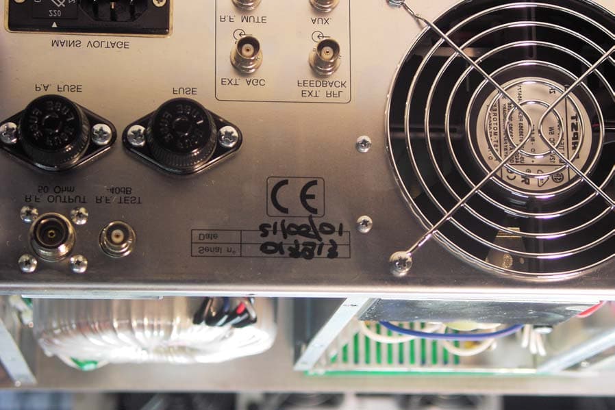
Click to zoom
Application Details
- Equipment Class
- TBC - Licensed Broadcast Station Transmitter
- Date of Grant
- Jul 06, 2004
- Application Purpose
- Original Equipment
- Date of Application
- Feb 03, 2004
- Equipment Note
- XT 150 Frequency agile FM Transmitter
- Frequency Range
- 88.00000000 - 108.00000000
- Company
- BEXT Inc
- Country
- United States
Documents & Files
Document Text
Text extracted from the exhibit documents filed with the FCC. Open a document above to read the original.
Users Manual
TECHNICAL AND MAINTENANCE MANUALTECHNICAL AND MAINTENANCE MANUAL TECHNICAL AND MAINTENANCE MANUALTECHNICAL AND MAINTENANCE MANUAL TECHNICAL AND MAINTENANCE MANUAL XT 150 & XT 150/S BEXT Inc. - 1045 TENTH AVE. - SAN DIEGO, CA 92101 USA (619) 239-8462 - FAX (619) 239-8474 http://www.bext.com - e-mail: [email protected] XT150 and XT150S Technical and Maintenance Manual Pag. 2 INDEXINDEX INDEXINDEX INDEX SECTION 1 General Description Pag. 4 Electrical Specifications (Table A) Pag. 6 Dimensional & Environmental Specifications (Table B) Pag. 8 SECTION 2 Electrical Description Pag. 9 Front Panel's View Description (Stereo Version) Pag. 12 Front Panel's View (Fig. 1A) Pag. 14 Front Panel's View Description (Mono Version) Pag. 13 Front Panel's View (Fig. 1B) Pag. 15 Rear Panel's View Description Pag. 16 Rear Panel's View (Fig. 2) Pag. 17 Block Diagram (Fig. 3) Pag. 18 Top's View Description Pag. 19 Top's View (Fig. 4) Pag. 20 Down's View Description Pag. 21 Upper's View (Fig. 5) Pag. 22 Recommend Test Equipment (Table C) Pag. 23 SECTION 3 Installation Procedures Pag. 24 SECTION 4 Maintenance Procedures Pag. 29 SECTION 5 Calibration Procedure of Modules Pag. 36 APPENDIX A Circuit Diagram, Bills of Material and Layouts Pag. 46 Wiring DiagramsPag. 47 Audio Input CardPag. 50 Frequency Selector Card (Mod. TSW-1) Pag. 54 XT150 and XT150S Technical and Maintenance Manual Pag. 3 Frequency Selector Card (Mod. TSW-3) Pag. 58 VCO CardPag. 62 PLL CardPag. 70 Alarms CardPag. 78 Meter CardPag. 83 Transformer Supply Section Pag. 88 Main Power SupplyPag. 91 Switching 1 Power Supply Pag. 95 Switching 2 Power Supply Pag. 99 Mono/MPX CardPag. 103 Stereo Coder Card (Mod. SDC30) Pag. 109 R.F. Power Amplifier Pag. 116 Low Pass Filter Card Pag. 120 Directional Coupler Card Pag. 124 Clipper CardPag. 128 150PS2 CardPag. 132 Stereo Coder Card (Mod. SDC30A002) Pag. 136 TCXO CardPag. 151 XT150 and XT150S Technical and Maintenance Manual Pag. 4 CHAPTER 1 GENERAL DESCRIPTIONGENERAL DESCRIPTION GENERAL DESCRIPTIONGENERAL DESCRIPTION GENERAL DESCRIPTION 1.0 INTRODUCTION1.0 INTRODUCTION 1.0 INTRODUCTION1.0 INTRODUCTION 1.0 INTRODUCTION This manual gives necessary information about XT150 and XT150S exciter. When referring to the Mono or Stereo Version, it will be duly noted. 1.1 GENERAL DESCRIPTION1.1 GENERAL DESCRIPTION 1.1 GENERAL DESCRIPTION1.1 GENERAL DESCRIPTION 1.1 GENERAL DESCRIPTION The XT150 is housed in a 3U, 19" rack-mouting container comprising a number of interconnected modules mounted internally on the main chassis, facilitating removal and substitution.The power output control, audio input level control and analog meter for the measurement of operating parameters, are all mounted on the front panel. The line power, audio input, RF output and telemetry (optional) connectors are mounted on the rear panel. 1.2 ELECTRICAL DESCRIPTION1.2 ELECTRICAL DESCRIPTION 1.2 ELECTRICAL DESCRIPTION1.2 ELECTRICAL DESCRIPTION 1.2 ELECTRICAL DESCRIPTION The XT150 is an exciter working in the 87.5 to 108 MHz band, programmable in steps of 10KHz. Its power output is continuously adjustable from 10W to 150W into a 50 Ohm load. The XT150 incorporates a stereo coder which guarantees excellent stereo separation together with low harmonic distortion (only for Stereo version). It also accepts two SCA signals. A front panel switch allows stereo operation (only for stereo version) or "mono/mpx" operation which excludes the stereo encoder and uses the "right" input as the mono input and the "left" input as the wideband composite input. The specification features low audio distortion and intermodulation figures (typically 0.03%) and a high signal-to-noise ratio (typically -80 dB). A voltage selector on the transformer primary allows a variety of supply voltages to be used. 1.3 METERS AND INDICATORS1.3 METERS AND INDICATORS 1.3 METERS AND INDICATORS1.3 METERS AND INDICATORS 1.3 METERS AND INDICATORS The operating parameters of the exciter can be monitored using the analog multimeter (12 Fig.1A and 8 Fig.1B) situated on the front panel. The parameter to be measured is selected by the rotary selector (11 Fig.1A and 7 Fig.1B). The frequency control (10 Fig.1A and 14 FIg.1B) allows frequencies to be selected in steps of 10KHz. Three red alarm leds indicate VCO unlock (15 Fig.1A and 11 Fig.1B), excess VSWR on the output and the excess of temperature (4 Fig.1A and 8 Fig.1B), and the shutdown condition, programmed by a remote command (10 Fig.1A and 6 Fig.1B). Three green leds (7 Fig.1A and 3 Fig.1B) indicate the presence of +12V, +15V and +28V voltages which are used to power the various cards inside the exciter. A selector (2 Fig.1A) allows selection between Mono/MPX and Stereo functions and another selector (6 Fig.1A and 2 Fig.1B) is provided to choose the level of the input signal. Trimmers are provided for adjustment of left and right channels (5 Fig.1A and 1 Fig.1B) and a switch allows the stereo subcarrier to benabled or disabled (3 Fig.1A). 1.4 AUTOMATIC FREQUENCY CONTROL1.4 AUTOMATIC FREQUENCY CONTROL 1.4 AUTOMATIC FREQUENCY CONTROL1.4 AUTOMATIC FREQUENCY CONTROL 1.4 AUTOMATIC FREQUENCY CONTROL The operating frequency is governed by a thermally-compensated, reference XT150 and XT150S Technical and Maintenance Manual Pag. 5 oscillator working within a phase-locked loop (PLL). The XT150 reaches frequency lock within a maximum of 30 seconds. 1.5 CONTROL CIRCUITS1.5 CONTROL CIRCUITS 1.5 CONTROL CIRCUITS1.5 CONTROL CIRCUITS 1.5 CONTROL CIRCUITS The control circuits allow automatic control of output power(internal and external), maintaining the chosen power level across the entire operating band. Furthermore another circuit protects the final stage against excessive VSWR or short circuits and excessive temperature. Then, there are other protection circuits that allow to limit the maximum output power and to protect the equipment against a power supply's overvoltage. 1.6 R.F. AMPLIFIER1.6 R.F. AMPLIFIER 1.6 R.F. AMPLIFIER1.6 R.F. AMPLIFIER 1.6 R.F. AMPLI…
Text truncated - open the document above for the full version.
Block Diagram
XT150 and XT150S Technical and Maintenance Manual Pag. 18 MONO VERSION BLOCK DIAGRAM (FIG.3A)MONO VERSION BLOCK DIAGRAM (FIG.3A) MONO VERSION BLOCK DIAGRAM (FIG.3A)MONO VERSION BLOCK DIAGRAM (FIG.3A) MONO VERSION BLOCK DIAGRAM (FIG.3A) STEREO VERSION BLOCK DIAGRAM (FIG.3B)STEREO VERSION BLOCK DIAGRAM (FIG.3B) STEREO VERSION BLOCK DIAGRAM (FIG.3B)STEREO VERSION BLOCK DIAGRAM (FIG.3B) STEREO VERSION BLOCK DIAGRAM (FIG.3B)
Cover Letter(s)
TO: Mr. Stanley Lyles FCC Equipment Authorization Branch FROM: David Petrik Bext Inc. Applicant: Bext Inc. FCC ID: E6T072503FMW150 Correspondence Reference No.: 26839 731 Confirmation No.: EA263366 Date of Correspondence: 6/28/2004 Subject: FCC Equipment Authorization System We, Bext Inc., hereby declare that we do not wish to register the XT 150 FM Exciter/Transmitter equipment under Part 74 of Title 47 per the Code of Federal Regulations. Sincerely, David Petrik Bext Inc. TEL 619-239-8462 FAX 619-239-8474 Email [email protected]
External Photos
Front Panel Back Panel Back Panel (Serial Number)
ID Label/Location Info
FCC ID : E6TØ725Ø3FMW15Ø BEXT INC.
ID Label/Location Info
The FCC ID Label is located on the right side of the XT 150 transmitter unit while facing the front panel of the transmitter unit. It is placed on the upper right hand corner (closer to the back panel of the XT 150 unit) of the side of which the FCC ID Label is placed.
ID Label/Location Info
To: Jaunice Green From: Bext Inc. Correspondence Ref No.: 26370 FCC ID: E6T072503FMW150 Date: March 5 th , 2004 Please explain and provide detail description of “FCC ID Label Location” request. We have re-submitted the FCC ID label location picture along with the description of its location per your request, however not yet satisfied the requirement. We will submit additional document/information after your explanation of the above mentioned request. Your prompt reply will be greatly appreciated.
Internal Photos
Top View Top View (PA) Bottom View Bottom View (Left) Bottom View (Right)
Operational Description
XT150 and XT150S Technical and Maintenance Manual Pag. 24 CHAPTER 3 INSTALLATION PROCEDURESINSTALLATION PROCEDURES INSTALLATION PROCEDURESINSTALLATION PROCEDURES INSTALLATION PROCEDURES 3.1 INTRODUCTION3.1 INTRODUCTION 3.1 INTRODUCTION3.1 INTRODUCTION 3.1 INTRODUCTION This chapter contains the information required for installation of the TEX150 exciter and for preliminary checks. 3.2 UNPACKING3.2 UNPACKING 3.2 UNPACKING3.2 UNPACKING 3.2 UNPACKING Remove the unit from its packaging and before any other operation, check for any damage that the unit may have suffered in transit and that all front and rear panel controls are functioning. 3.3 INSTALLATION3.3 INSTALLATION 3.3 INSTALLATION3.3 INSTALLATION 3.3 INSTALLATION 1)Check that the line voltage selector is correctly set for the local supply. If not, remove the cover on which the voltages are printed and rotate it until the required value corresponds to the arrow, and reinsert it. Check also that the fuse (1 Fig.2) mounted inside the cover is present and in order. The current capacity of the fuse are as follows: 220-240 V - 6.3 A 100-120 V - 12 A 2)Now ensure that the PWR ADJ control (9 Fig.1A or 5 Fig.1B) is rotated fully anti-clockwise, using a small screwdriver. N.B. The control is a ten-turn potentiometer so care should be taken to verify the minimum position. Units are usually shipped with this control already at minimum. WARNING: When the unit is switched on with the control at its minimum position, power output is about 10W. 3)Connect a dummy load with a power rating of at least 150 W continuous to the RF output, situated on the rear panel of the unit. It is advisable to connect a bypass wattmeter in series with this load in order to verify the accuracy of the unit's own internal wattmeter (see SETUP 1). SETUP 1SETUP 1 SETUP 1SETUP 1 SETUP 1 XT150 DUMMY LOAD XT150 and XT150S Technical and Maintenance Manual Pag. 25 4)Connect a switch, via a cable, to the REMOTE 3 connector (4 Fig.2) on the rear panel so that the switch is able to short the central conductor to its screen. Leave the switch in the short-circuit position. 5)Switch the unit's ON/OFF switch (13 Fig.1A or 9 Fig.1B) to the OFF position. 6) Connect line power to the unit via the VDE socket (2 Fig.2). Note: It's essential that the unit be properly earthed to ensure both the safety of the operator as well as the correct functioning of the equipment. 7)Switch the power On switch (13 Fig.1A or 9 Fig.1B) to the ON position and check that the three green internal voltage led (7 Fig.1A or 3 Fig.1B) and the red UNLOCK led (15 Fig.1A or 11 Fig.1B) are all on. Select the desired operating frequency using the corresponding selector. The red UNLOCK led should switch off within 30 seconds, indicating that the oscillator has locked onto the operating frequency. The frequency se- lector comprises five figures of which the three to the left of the decimal point represent (from left to right) hundreds of MHz, tens of MHz and MHz. The two figures to the right of the decimal point rep- resent (from left to right) hundreds of KHz and tens of KHz. Eg: 098.45 = ninety eight megahertz and four hundred and fifty Kilohertz. Eg: 103.94 = one hundred and three Megahertz and nine hundred and forty Kilohertz. Furthermore, if a frequency is selected beyond the two limits of the 87.5-108 MHz band, the amplifier will continue to work even through the displayed frequency no longer corresponds to the operating frequency of the unit. Note: Transmitting outside the legal band (87.5-108 MHz) is an offenceNote: Transmitting outside the legal band (87.5-108 MHz) is an offence Note: Transmitting outside the legal band (87.5-108 MHz) is an offenceNote: Transmitting outside the legal band (87.5-108 MHz) is an offence Note: Transmitting outside the legal band (87.5-108 MHz) is an offence and may lead to prosecution.and may lead to prosecution. and may lead to prosecution.and may lead to prosecution. and may lead to prosecution. 8)After having verified that the UNLOCK led is switched off and that the unit is therefore locked to the selected operating frequency, switch the switch connected to the REMOTE connector so as to remove the short circuit between the central conductor and ground. The RF output is now enabled and should correspond to a power level of about 10W. To check this reading, select FWD on the meter selector and read the power from the 200 W FSD scale. 9)Using a small screwdriver, rotate the PWR ADJ control clockwise; the power output should increase progressively to a maximum of 100W. Check the value with the bypass wattmeter which should be within ±10%. XT150 and XT150S Technical and Maintenance Manual Pag. 26 10)With the power output at 150W, select a new operating frequency well away from the current value. Eg: 107 MHz: the UNLOCK led should switch on and the power output should fall to zero at the same time. Only when the UNLOCK led switches off (unit locked to new frequency) should the power output resume its previous level. 11) Automatic power control check It is advisable to start this procedure with the operating frequency set to 87.50 MHz. When locked to this frequency, the PWR ADJ control should be adjusted for an output power of 50 W. Now, with no further adjustment of the PWR ADJ control, change the operating frequency in steps of 4-5 MHz, ensuring that the output power remains constant at 50 W. 12) SWR alarm check For this test, adjust the PWR ADJ control for a power output of 10W. Disconnect the output load and check that the S.W.R. led switches on. Now adjust the PWR ADJ control to check that the unit switches on again at a reflected power level of about 20 W. Turn the PWR ADJ control for maximum power and check that the reflected power does not exceed 50 W. Re-connect the output load and check that REF falls to zero, the SWR led switches off and that PWR FWD jumps to 150 W. 13) Now short circuit the central conductor of the REMOTE input to ground and the output power should drop instan…
Text truncated - open the document above for the full version.
Parts List/Tune Up Info
2.1 INTRODUCTION This section describes, in detail, the operating theory behind the XT300. To aid understand- ing, the unit has been subdivided into blocks, each of which is fully described below. The block diagram is shown in Fig. 3 2.2 POWER SUPPLY This circuit comprises a board, mounted on a heat sink, which is fixed to the central part of the lower section of the unit. The power supply generates the various modules that make up the XT300. The transformer has a selectable input from 110V to 240V and three outputs: A. 30/0/30V (9A), B. 36V (0.5A), and C. 20V (1A). This power supply is composed of two main parts: after having undergone filtering for mains- borne interference, the supply is transformed into four lower voltages, rectified, smoothed and stablized to the following values: +12V, +15V +15 variable and +50V to obtain the higher efficiency switching power supply (85-90%). The +15V supplies the encoder mixer, the PLL card, the VCO card, the meter card and the alarms card. The +12V supplies the fan . The +15V variable supplies the input of the RF power module amplifier driver (BLF244) and the 50V supplies the final power stage (BLF278). The variable voltage of the final stage driver is controlled by the PWR ADJ control which determines the RF power output of the exciter. The automatic control of the output power guarantees the power level set by the PWR ADJ control right across the frequency range and independently of the other variables such as temperature, load variations etc. The system works by comparing the value set by the PWR ADJ control with the actual power output of the unit and compensating accordingly. 2.3 AUDIO INPUT CARD This card is situated on the rear panel of the exciter. The card filters all audio signal inputs to the unit, removing RF interference, before supplying them to the encoder mixer or mono/mpx card. The main operating parameters of the exciter are available for remote monitoring via the telemetry connector. 2.4 STEREO CODER CARD (only for Stereo Version) This card is situated in the lower part of the unit. ELECTRICAL DESCRIPTION The card can function either as a stereo encoder or as a simple mixer for the various audio inputs. The function may be selected by a control situated on the front panel. In the stereo encoder mode, the 19 KHz pilot tone is derived from a quartz crystal reference oscillator. So too is the sampling frequency which allows the L and R sig- nals to be separated from the multiplexing signal. Plus the suppresion of the 38 KHz frequency. The level of the left and right signals are set by the corresponding selector situated on the front panel. The signals are filtered at 15 KHz and pre-emphasized (50 uS CCIR, 75 uS FCC) before being sent to the multiplexing circuit. The audio signals from the two SCA inputs are mixed in to provide the output. In the mixer mode (Mono/Mpx) the stereo encoder is bypassed, the right input accepts a mono signal and the left input accepts a multiplex signal up to 100 KHz. The SCA inputs remain un- changed. Three rectifiers allow the peak levels of the two inputs “Left/MPX” and “RIGHT/MONO” to be displayed on the analog meter, and provide the audio detector circuit with the deviation level. 2.5 PLL CARD The PLL card is situated internally, in the upper part of the unit. The circuit includes a reference crystal oscillator (optional high stability), a logic section that includes the frequency dividers and comparator. The reference crystal oscillator gener- ates a 4 MHz frequency that is divided to generate a fixed 1 KHz signal. This signal is compared to the operating frequency generated by the VCO divided based on the frequency set on the contraves board. An indicator situated on the front panel signals the “unlocked” condition. The comparator output (AFC signal) is sent to the varicap diodes situated on the VCO card. 2.6 VCO CARD The VCO card is situated internally, in the upper part of the unit. This module includes an audio input stage at low frequency, a voltage controlled oscillator (VCO) and driver stage. The audio signal supplied by the encoder mixer is amplified and then injected into the VCO to provide class F3 modulation. The voltage controlled oscillator (VCO) generates the signal on the frequency set on the contraves. This signal is amplified to 300mW level (25dBm) to drive the final stage and sent to the PLL circuit situated on the PLL card. The operating frequency generated by the VCO is divided down before being compared to a reference frequency, generated by a high stability oscillator (stan- dard 5 ppm). The error voltage is filtered and used to compensate the VCO frequency and guarantee its stability. A trimmer is present on this card for adjustment of deviation. 2.7 RF POWER AMPLIFIER The final power stage is mounted on a heat sink to dissipate waste heat and is en- closed in a totally screened metal container, fixed to the upper-middle part of the central section of the unit. The RF signal coming from the stereo decoder or Mono/ MPX at a power level of about 300mW, reaches the driver stage (BLF244) and is amplified to a level from about 300mW to 8W before being further amplified by the final stage (BLF278) to a level of up to 300W. The resultant signal is then filtered by a low-pass filter which removes any harmonic content. A directional coupler allows the direct and reflected power levels to be measured and displayed on the analog multim- eter and fedback to the power supply for automatic control of the output power (see power supply description). A BNC connector situated on the rear panel provides a power signal at -60db of the amplifier output power. 2.8 METER CARD This card is situated centrally on the front panel. The card receives direct and reflected power signals from the power supply which, in turn, come from the final power stage. The stereo encoder card supplies deviation and left and right signal lev- els. These signal levels are then displayed on the analog meter according to…
Text truncated - open the document above for the full version.
Schematics
XT150 and XT150S Technical and Maintenance Manual Pag. 44 SETUP 11 XT150 and XT150S Technical and Maintenance Manual Pag. 45 F) Maximum Output Power Adjustment Can be necessary to set maximum output power at maximum value included between 10 and 150W. 1)Connect a 50 ohm, 300W dummy load to the RF output. 2)Adjust output power at minimum turning PWR ADJ trimmer (9 Fig.1A or 5 Fig.1B) completely anticlockwise and then switch on the equipment. 3)Increase output power until 150W turning PWR ADJ trimmer (9 Fig.1A or 5 Fig.1B) clockwise. 4)Turn trimmer R44, until to have maximum output power presetted on external wattmeter. 5)Then, adjust output power turning PWR ADJ trimmer (9 Fig.1A or 5 fig.1B) and note that output power can be increased over presetted value. NOTE: The jumpers shown in table , disable all protections (all enabled from firm). A no-correct use of these jumpers can cause seroius damage to the unit and will automatically make the warranty void. ALARMS CARD TRIMMERS AND JUMPERSALARMS CARD TRIMMERS AND JUMPERS ALARMS CARD TRIMMERS AND JUMPERSALARMS CARD TRIMMERS AND JUMPERS ALARMS CARD TRIMMERS AND JUMPERS REF.REF. REF.REF. REF. DESCRIPTIONDESCRIPTION DESCRIPTIONDESCRIPTION DESCRIPTION R2 Internal AGC Adjustment R7 Max Power Output Adjustment (VSWR INFINITE) R12 External VSWR Threshold Adjustment R16 External AGC Adjustment R23 Temperature Threshold Adjustment R25 Temperature Led Lighting Adjustment R44 Max Power Output Adjustment JP1 Internal AGC Insertion (DON'T REMOVE) JP2 Internal AGC Insertion (DON'T REMOVE) JP3 External VSWR Insertion JP4 External AGC Insertion JP5 Temperature Threshold Insertion JP6 Maximum Output Power Threshold Insertion XT150 and XT150S Technical and Maintenance Manual Pag. 46 APPENDIX A CIRCUIT DIAGRAMS, LAYOUTS AND BILLS OF MATERIALCIRCUIT DIAGRAMS, LAYOUTS AND BILLS OF MATERIAL CIRCUIT DIAGRAMS, LAYOUTS AND BILLS OF MATERIALCIRCUIT DIAGRAMS, LAYOUTS AND BILLS OF MATERIAL CIRCUIT DIAGRAMS, LAYOUTS AND BILLS OF MATERIAL This section contains circuit diagrams, layouts and bills of material of the modules which composing the equipment. For more information about each module see as reference Section 2. XT150 and XT150S Technical and Maintenance Manual Pag. 47 WIRING DIAGRAMWIRING DIAGRAM WIRING DIAGRAMWIRING DIAGRAM WIRING DIAGRAM 1 Mono/MPX Version Pag. 49 2 Stereo Version Pag. 48 XT150 and XT150S Technical and Maintenance Manual Pag. 48 XT150 and XT150S Technical and Maintenance Manual Pag. 49 XT150 and XT150S Technical and Maintenance Manual Pag. 50 AUDIO INPUT CARDAUDIO INPUT CARD AUDIO INPUT CARDAUDIO INPUT CARD AUDIO INPUT CARD 1 Circuit Diagram Pag. 51 2 Bill of Materials Pag. 52 3 Component Layout Pag. 53 XT150 and XT150S Technical and Maintenance Manual Pag. 51 XT150 and XT150S Technical and Maintenance Manual Pag. 52 Audio Input Card Bill Of Materials Page 1 Item Quantity Reference Part Description Part Order Code ____________________________________________________________________________________________________ 1 4 R3,R4, 1K RESISTOR 1/4W 5% RSC1/4JK0001 R5,R6 2 12 C1,C2,C3, 33pF CERAMIC CAPACITOR NP0 CKM330BJ600C C4,C5,C6, C7,C8,C9, C10,C11,C12 3 8 C13,C14, 0.1uF CERAMIC CAPACITOR CKM104BK600P C15,C16, C17,C18, C19,C20 4 6 L1,L2,L3, VK RF CHOKE IMPVK00A L4,L5,L6 5 2 EC1,EC2 XLRFTL XLR FEMM. DA TELAIO CNTXLRFP3P 6 1 EC3 MORSET. 10 MORSETT. TEL. 10 CONT. MORSP10P 7 2 CN1,CN2 26 P CONN. CONN. M 2*13 P 2.54 CNTMCSFC26P 8 2 BNC1,BNC2 BNC IS.CS. CONN. BNC A STAMP. IS. CNTBNCFCSIS 9 10 H1,H2,H3, WIRE JUMP. PONTICELLO A FILO WIREJUMPER H4,H5,H6, H7,H8, H9,H10 10 8 R1,R2,R7, N.C. NOT CONNECTED R8,C21,C22, C23,C24 XT150 and XT150S Technical and Maintenance Manual Pag. 53 XT150 and XT150S Technical and Maintenance Manual Pag. 54 FREQUENCY SELECTOR CARD (Mod. TSW-1)FREQUENCY SELECTOR CARD (Mod. TSW-1) FREQUENCY SELECTOR CARD (Mod. TSW-1)FREQUENCY SELECTOR CARD (Mod. TSW-1) FREQUENCY SELECTOR CARD (Mod. TSW-1) 1 Circuit Diagram Pag. 55 2 Bill of Materials Pag. 56 3 Component Layout Pag. 57 XT150 and XT150S Technical and Maintenance Manual Pag. 55 XT150 and XT150S Technical and Maintenance Manual Pag. 56 Frequency Selector Card Mod. TSW-1 Bill Of Materials Page 1 Item Quantity Reference Part Description Part Order Code ____________________________________________________________________________________________________ 1 1 CN1 26 P CONN. CONN. M 2*13 P 2.54 CNTMCSFC26P 2 5 CNTR1, CONTRAVES COMMUTATORI BCD 15mm COMBCD15 CNTR2, CNTR3, CNTR4, CNTR5 3 2 D1,D2 1N4148 SILICON DIODE DIS1N4148 4 1 D3 LED-R5 RED LED DIODE LEDRO05 XT150 and XT150S Technical and Maintenance Manual Pag. 57 XT150 and XT150S Technical and Maintenance Manual Pag. 58 FREQUENCY SELECTOR CARD (Mod. TSW-2)FREQUENCY SELECTOR CARD (Mod. TSW-2) FREQUENCY SELECTOR CARD (Mod. TSW-2)FREQUENCY SELECTOR CARD (Mod. TSW-2) FREQUENCY SELECTOR CARD (Mod. TSW-2) 1 Circuit Diagram Pag. 59 2 Bill of Materials Pag. 60 3 Coponent Layout Pag. 61 XT150 and XT150S Technical and Maintenance Manual Pag. 59 XT150 and XT150S Technical and Maintenance Manual Pag. 60 Frequency Selector Card Mod.T SW-3 Bill Of Materials Page 1 Item Quantity Reference Part Description Part Order Code ____________________________________________________________________________________________________ 1 1 CN1 26 P CONN. CONN. M 2*13 P 2.54 CNTMCSFC26P 2 5 CNTR1, CONTRAVES COMMUTATORI BCD 15mm COMBCD15 CNTR2, CNTR3, CNTR4, CNTR5 3 2 D1,D2 1N4148 SILICON DIODE DIS1N4148 4 1 D3 LED-R5 RED LED DIODE LEDRO05 5 1 U1 27512 65,536x8 B CMOS EPROM CID27512 XT150 and XT150S Technical and Maintenance Manual Pag. 61 XT150 and XT150S Technical and Maintenance Manual Pag. 62 VCO CARDVCO CARD VCO CARDVCO CARD VCO CARD 1 A.F. Section Circuit Diagram Pag. 63 2 A.F. Section Bill of Materials Pag. 64 3 R.F. Section Circuit Diagram Pag. 65 4 R.F. Section Bill of Materials Pag. 66 5 VCO Component Layout Pag. 69 XT150 and XT150S Technical and Maintenance Manual Pag. 63 XT150 and XT150S Technical and Maintenance Manual Pag. 64 VCO Card - A.F. Section Bill Of Mat…
Text truncated - open the document above for the full version.
Test Report
Test Report on the XT 150 (150 Watt FM Transmitter unit) per FCC Certification Approval Process Prepared by BEXT Inc. Jan. 2004 0 INTRODUCTION This test report serves the purpose of providing test result and measurement information for the Federal Communications Commission Certification (FCC) Approval Process. Certification of the equipment unit is based on the representations and test results submitted by the manufacturer to the FCC, as described in FCC ruling Part 2.907 subpart (a). The XT 150 FM Transmitter is comprised of several interconnected modules mounted internally on the main chassis, facilitating removal and substitution. The Power Output Control, Audio Input Level Control and Analog Meter for measurement of the operating parameters are all mounted on the front panel of this transmitter unit. The AC Power Line, Audio Input, RF Output and Telemetry Connectors are mounted on the rear panel of this transmitter unit. The test results presented in this report are generated from the laboratory of Bext Inc., generated from testing took place between January 27 th , 2004 to February 4 th , 2004. 1 TABLE OF CONTENT I. Tests a. FM Transmission System Requirements b. Frequency Stability c. Carrier Frequency Departure Tolerance at Warm Up Period d. Conducted Harmonics e. Carrier Frequency Departure Tolerance with Temperature II. Statement of Conformity GENERAL NOTES This manual serves the purpose of interpreting the Federal Communications Commission regulations, and to provide instructions for duplicating all test measurements within this manual. For “Equipment Authorization”, the FCC requires the manufacturer to complete the tests and keep test records on file for two years after the last equipment is manufactured. The FCC also requires the users and customers to verify periodically that the authorized equipment unit is compliant, also that the certifications attached to the equipment units subsequently marketed by the authorization grantee are identical to the sample equipment unit tested, as “identical” is defined in the FCC ruling Part 2.908. In the case of an FCC agent requires to conduct an inspection or visit to the user’s site, they will require an Owner’s Manual that is supplied with every equipment unit (XT 150). The instructions for these tests are written for the clarification to the customers of the testing procedures and to reproduce the tests. 2 TESTING CONDITIONS The conditions of the laboratory and equipment setting are listed as follow: A) The Testing Frequency of the XT 150 was set in the center of the band at 98MHz, along at 88 MHz and 108 MHz for comparable results. B) The Output Power of the XT 150 was at 150 Watts throughout the entire testing process. C) An AC input of 117 vac was implemented during the testing of the XT 150 unit. D) All Audio Signal Levels were made with a function generator, with output selection at 600 ohms, connected to the XT 150 unit in parallel with a 50 ohm Load. If an Audio Generator is used, then a 600 ohm Load should be used. BLOCK DIAGRAM of CERTIFICATION TEST PROCEDURE * For details of the equipments please see the next section. 3 EQUIPMENT LIST (USED FOR CERTIFICATION TEST PROCEDURE) 1) 600 Ω Low Distortion Audio Generator Brand: Hameg Model: HM 8037 Last Calibration: 04/09/2003 2) 150W FM Transmitter Brand: Bext Model: XT 150 3) 50 ohm Watt Meter Brand: Bird Model: 43P Last Calibration: 04/25/2003 4) 20-1000MHz Sample Take-Off Brand: Bird Model: 4275 5) 0.5W VHF Attenuator Brand: Hewlett Packard Model: 355C 6) –40 dBm Band Stop Filter Brand: RVR Model: B.S. 7) RF Spectrum Analyzer Brand: Aicom Model: 3030TG Last Calibration: 09/24/2003 8) 600W RF Dummy Load Brand: Bird Model: 8401 *The Equipment Devices listed below are not shown in the block diagram of previous section. 9) Climate Temperature Chamber Brand: A.C.S. Model: TY56010 10) Thermometer Brand: Wavetek Model: Meterman 37XR Last Calibration: 11/03/2003 11) Frequency Counter Brand: Rohde & Schwarz Model: FMAB Last Calibration: 04/11/2003 4 MEASUREMENT TECHNIQUES All measurements are made with the steady output power of 150 watts fr…
Text truncated - open the document above for the full version.
Contact Information
Applicant
Dennis Dionigi Pieri(CEO)
Technical Contact
Bext Inc.David A Petrik
[email protected]6196853918
1045 Tenth Avenue · San Diego, California · United States
Non-Technical Contact
Bext Inc.Nikki Monfredo
[email protected]6192398462
Technical Specifications
| # | Rule Parts | Frequency Range | Power Output | Emission | Tolerance |
|---|---|---|---|---|---|
| 1 | 73 | 88 MHz - 108 MHz | 150 W | 300KF8E | 500.0000000000 Hz |
Other Applications from BEXT Inc
E6T000SF00250
Aug 02, 1994TBC - Licensed Broadcast Station Transmitter
Equipment Class
TBC - Licensed Broadcast Station TransmitterE6T000SF00100
Aug 02, 1994TBC - Licensed Broadcast Station Transmitter
Equipment Class
TBC - Licensed Broadcast Station TransmitterE6T000SF00400
Jul 31, 1994TBC - Licensed Broadcast Station Transmitter
Equipment Class
TBC - Licensed Broadcast Station TransmitterE6T000FMLEX25
Jul 04, 1994TBC - Licensed Broadcast Station Transmitter
Equipment Class
TBC - Licensed Broadcast Station TransmitterE6T000SF01000
Jul 04, 1994TBC - Licensed Broadcast Station Transmitter
Equipment Class
TBC - Licensed Broadcast Station Transmitter