EW789-5004-00900 MHz Cordless Telephone
VTech Telecommunications Ltd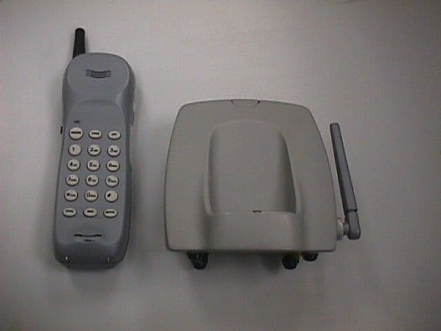
Click to zoom
Application Details
- Equipment Class
- DXX - Part 15 Low Power Communication Device Transmitter
- Date of Grant
- Jul 23, 2000
- Application Purpose
- Original Equipment
- Date of Application
- Jul 23, 2000
- Equipment Note
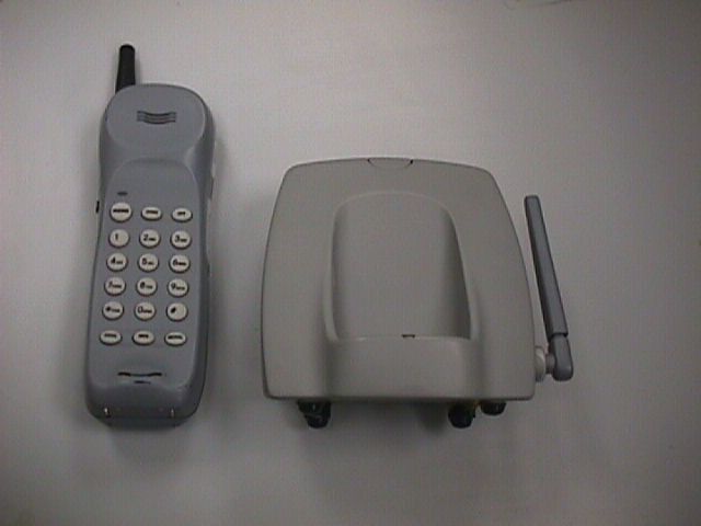
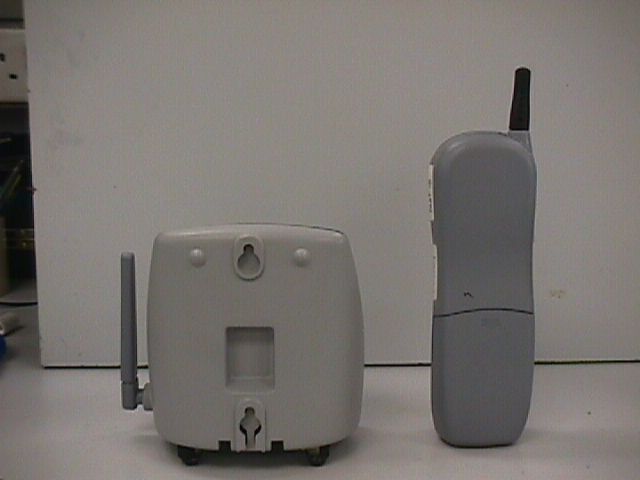
- 900 MHz Cordless Telephone
- Frequency Range
- 926.00000000 - 928.00000000
- Company
- VTech Telecommunications Ltd
- Country
- Hong Kong
Documents & Files
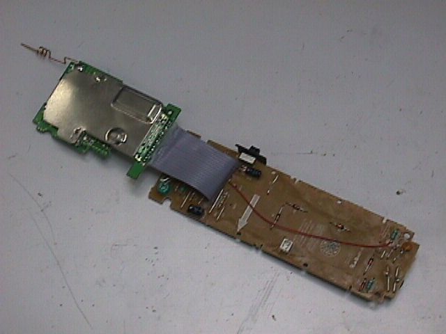
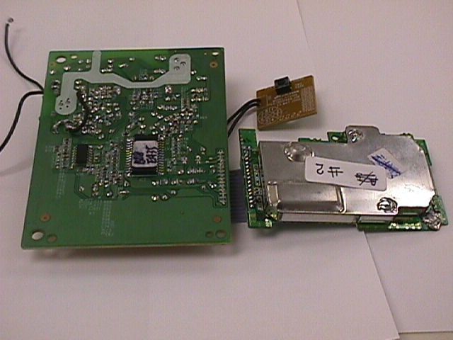
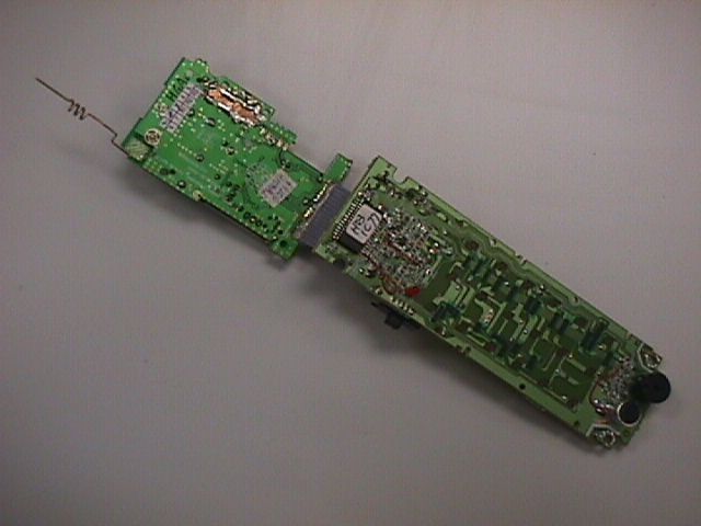
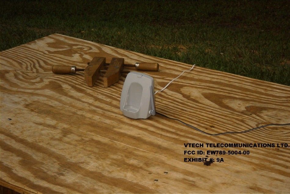
Document Text
Text extracted from the exhibit documents filed with the FCC. Open a document above to read the original.
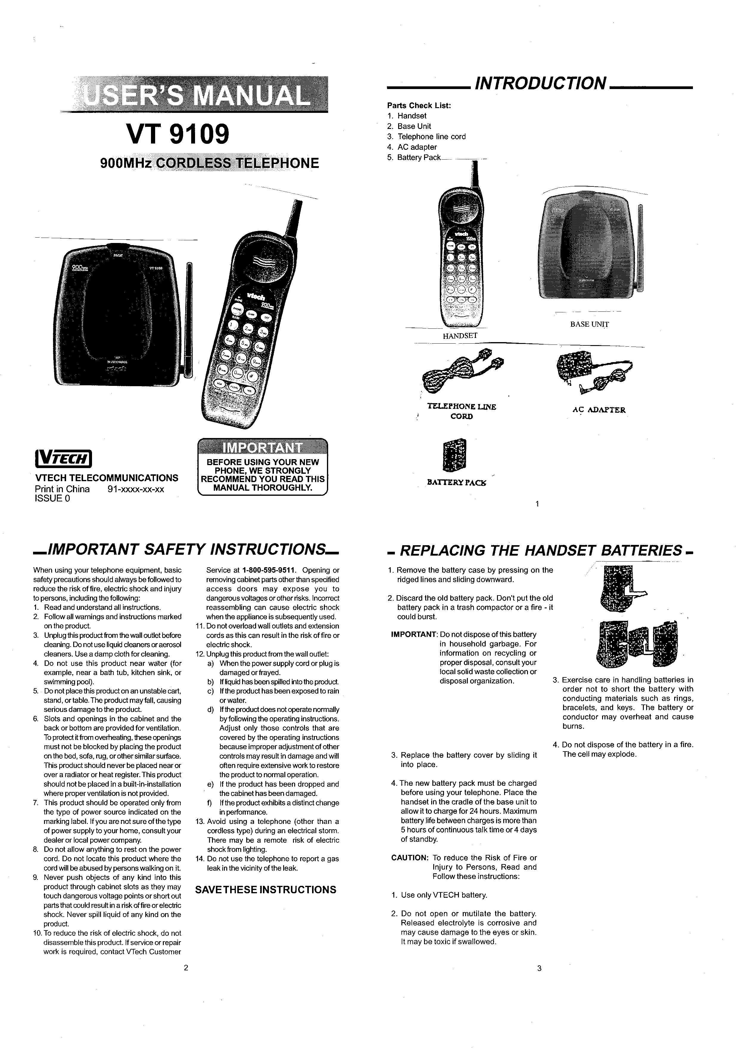
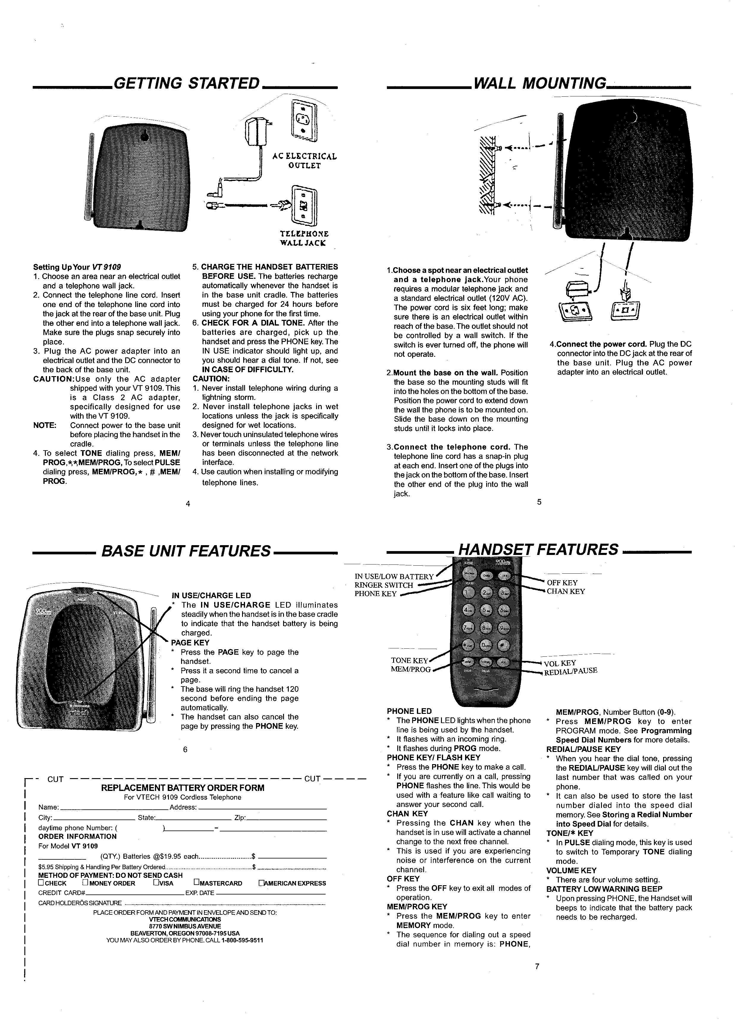
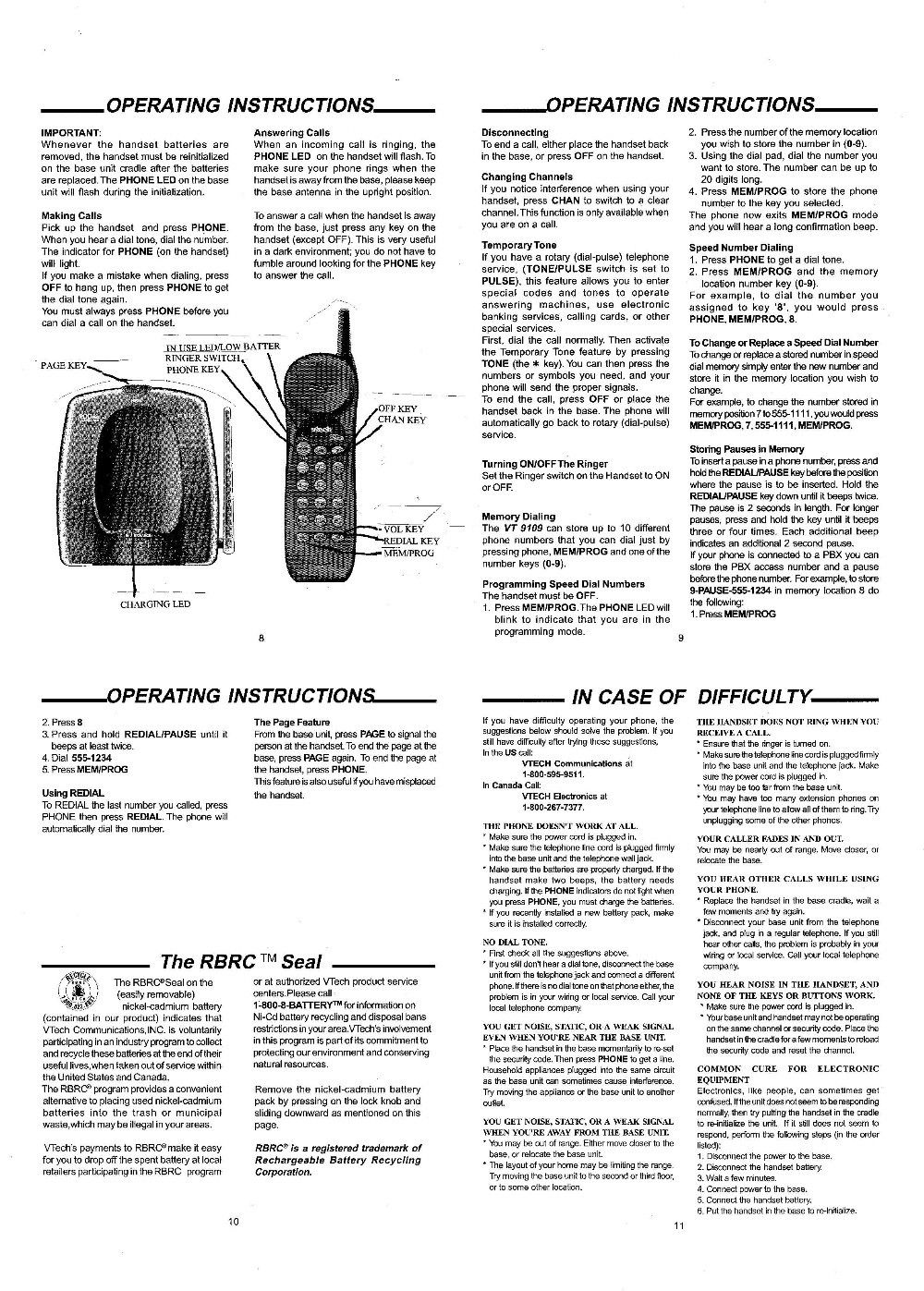
Users Manual
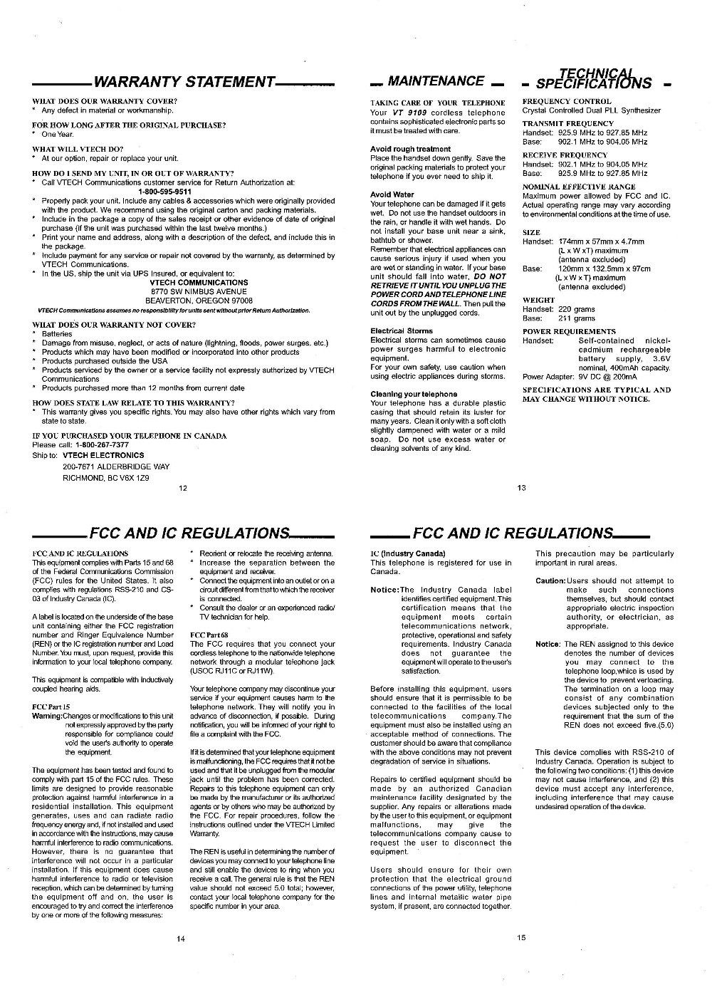
VTECH COMMUNICATIONS LTD. (TELECOM / R&D) File :Date :8-May-2000TITLE : INTERNAL PRODUCT SPECIFICATION DOCUMENT NO.REV.NO. 0 PAGE 1 of 14 This document is proprietary to VTech Communications Ltd. VTech HK R&D info.. Internal Product Specification for the VT 9109 BLK Basic Phone Revision History: RevisionDescriptionPageEffective Date 0Draft Release.All8 May 00 VTECH TELECOMMUNICATIONS LTD. FCC ID: EW789-5004-00 JOB #: 226AH0 EXHIBIT #: 5A VTECH COMMUNICATIONS LTD. (TELECOM / R&D) File :Date :8-May-2000TITLE : INTERNAL PRODUCT SPECIFICATION DOCUMENT NO.REV.NO. 0 PAGE 2 of 14 This document is proprietary to VTech Communications Ltd. VTech HK R&D info.. Contents 1.OVERVIEW...................................................................................................................................................3 1.1. G EN ERAL D ESCRIPTIO N ...............................................................................................................................3 1.2. R EGULATORY S TANDARDS ...........................................................................................................................3 1.3. P RELIMIN ARY F EATURE L IST ........................................................................................................................3 1.3.1.Basic Features..................................................................................................................................3 1.3.2.Unique Features ...............................................................................................................................3 1.3.3.Features Not Provided .....................................................................................................................3 1.4. C O SMETIC S TYLIN G .....................................................................................................................................4 1.4.1.Base Unit Line Drawing...................................................................................................................4 1.4.2.Handset Line Drawing .....................................................................................................................5 2.FUNCTIONAL LAYOUT.............................................................................................................................6 2.1. H ANDSET F UNCTIONAL L AYOUT ..................................................................................................................6 2.1.1.Handset LED Indicators...................................................................................................................6 2.1.2.Handset Key Descriptions................................................................................................................6 2.2. B ASE U NIT F UNCTIONAL L AYOUT ................................................................................................................7 2.2.1.Base Unit LED Indicators ................................................................................................................7 2.2.2.Base Unit Key Descriptions .............................................................................................................7 3.OPERATING MODES .................................................................................................................................8 3.1. STANDBY M ODE .......................................................................................................................................8 3.2. PHONE M ODE ............................................................................................................................................8 3.2.1.Dialing Methods...............................................................................................................................9 3.2.2.Redial Buffer ....................................................................................................................................9 3.2.3.Memory Dialing ...............................................................................................................................9 3.3. MEM M ODE ..............................................................................................................................................10 3.3.1.Speed Dial Programming ...............................................................................................................11 3.3.2.Tone/Pulse Select Programming....................................................................................................11 3.4. RINGING M ODE .......................................................................................................................................12 3.5. PAGE M ODE .............................................................................................................................................12 4.RF LINK OPERATION ..............................................................................................................................13 4.1. S ECURITY C ODE .........................................................................................................................................13 4.2. RF C HAN N EL S ELECTIO N ..........................................................................................................................13 4.2.1.Manual Channel Selection .............................................................................................................13 5.POWER MANAGEMENT.........................................................................................................................14 5.1. B ATTERY ...................................................................................................................................................14 5.2. L OW B ATTERY I NDICATION .......................................................................................................................14 VTECH TELECOMMUNICATIONS LTD. FCC ID…
Text truncated - open the document above for the full version.
Block Diagram
VT9109 BLOCK DIAGRAM OF B/U SECTION LNA IF Amp BUFFER 2ND LNA BPF RX VCO FILTER PLL Tx VCO DOUBLER RF P0-Amp AUDIO PRE-AMP. SAW DUPLEXER RX-Data Mixer MIC PER-AMP IF Demodulator Expandor Audio Amp CONTROL AN8953FA IF AMP BPF Compandor SQ SPLATTER TX Data RING-DET STB CLK Data RSSI MCU LINE INTERFACE 7/24/00 Prepared by : CHAN PO WAH 7/24/00 Prepared by : CHAN PO WAH
ID Label/Location Info
XXXX THIS DEVICE COMPLIES WITH PART 15 OF THE FCC RULES. OPERATION IS SUBJECT TO THE FOLLOWING TWO CONDITIONS: 1) THIS DEVICE MAY NOT CAUSE HARMFUL INTERFERENCE; AND 2) THIS DEVICE MUST THAT MAY CAUSE UNDESIRED OPERATION. ACCEPT ANY INTERFERENCE RECEIVED, INCLUDING INTERFERENCE PRIVACY OF COMMUNICATIONS MAY NOT BE ENSURED WHEN USING THIS PHONE. VTECH TELECOMMUNICATIONS LTD. MANUFACTURED IN CHINA COMPLIES WITH PART 68 FCC RULES FCC REGISTRATION NO.: XXXXXXX-XXXXX-XX-X RINGER EQUIVALENCE: XXXX USOC JACK: XXXX CANADA XXXX XXX XXXX REN/IES: XX IC:RSS/CNR210 HAC FCC ID: EW789-5004-00 CORDLESS TELEPHONE MODEL: 9109 DC9V 200mA, CLASS 2 POWER SOURCE ONLY Cd PR ODUCT CONT AINS NICKEL-CADMIUM BA TTER Y : MUST BE RECYCLED OR DISPOSED OF PR OPERL Y . DO NO T B URN OR PUNCTURE BA TTER Y . LIKE O THER BA TTERIES OF THIS TYPE. IF IT IS B URNED OR PUNCTURED . IT COULD RELEASE T O XIC MA TERIAL WHICH COULD CA USE INJUR Y . 9109 BASE-UNIT REAR VIEW CANADA XXXX XXX XXXA CAUTION USE ONLY VTECH BATTERY 80-5037-00-00 VT9109 HANDSET TOP VIEW (COMMON TO ALL COLOUR) FCC ID: EW789-5004-00 9109 HANDSET FRONT VIEW FILE: 9109-FCCID.AI DATE: 16JUN2000 REVISION: 5 FCC ID: EW789-5004-00 VT 9109 HANDSET FRONT VIEW XXXX THIS DEVICE COMPLIES WITH PART 15 OF THE FCC RULES. OPERATION IS SUBJECT TO THE FOLLOWING TWO CONDITIONS: 1) THIS DEVICE MAY NOT CAUSE HARMFUL INTERFERENCE; AND 2) THIS DEVICE MUST THAT MAY CAUSE UNDESIRED OPERATION. ACCEPT ANY INTERFERENCE RECEIVED, INCLUDING INTERFERENCE PRIVACY OF COMMUNICATIONS MAY NOT BE ENSURED WHEN USING THIS PHONE. VTECH TELECOMMUNICATIONS LTD. MANUFACTURED IN CHINA COMPLIES WITH PART 68 FCC RULES FCC REGISTRATION NO.: XXXXXXX-XXXXX-XX-X RINGER EQUIVALENCE: XXXX USOC JACK: XXXX CANADA XXXX XXX XXXX REN/IES: XX IC:RSS/CNR210 HAC FCC ID: EW789-5004-00 CORDLESS TELEPHONE MODEL: VT 9109 DC9V 200mA, CLASS 2 POWER SOURCE ONLY Cd PR ODUCT CONT AINS NICKEL-CADMIUM BA TTER Y : MUST BE RECYCLED OR DISPOSED OF PR OPERL Y . DO NO T B URN OR PUNCTURE BA TTER Y . LIKE O THER BA TTERIES OF THIS TYPE. IF IT IS B URNED OR PUNCTURED . IT COULD RELEASE T O XIC MA TERIAL WHICH COULD CA USE INJUR Y . VT 9109 BASE-UNIT REAR VIEW
Operational Description
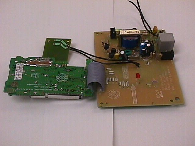
VT9109 Circuit Description : The following circuit description for model VT9109 is base on the circuit diagram and block diagram of VT9109. VT9109 Handset : 1. Receiving Path The receiving path is established by below sections. Low Noise Amplifier (LNA) FM signal filtering by the duplexer , and input to tuning amplifier Q555. Then input to 2 nd tuning amplifier Q512 before output to mixer . Mixer Mixer is included Q520 , and local oscillator Q506 & Q504 , which is controlled by the PLL U1 PLL pin . The IF (10.7MHz) is filtering by a ceramic filter CF501 , the filtered IF will input to IF amplifier U1 pin 40. IF amplifier IF amplifier is built in U1. Amplified IF is filtering again by a ceramic filter F1 , the filtered IF will input to FM demodulator U1 pin 33. FM demodulator and expandor The IF is demodulate by quadrate coil T1 , then the recovered audio is input to the expandor for de-emphasis , before output to the handset speaker though audio amplifier . 2. Transmitting Path The transmitting path is established by below sections. Mic amplifier and compressor Audio pick up by handset microphone is amplified by internal mic amplifier of U1 , then input to compressor for pre-emphasis , before input to the modulator (Tx VCO). VTECH TELECOMMUNICATIONS LTD. FCC ID: EW789-5004-00 JOB #: 226AH0 EXHIBIT #: 6A Modulator and Tx VCO The transmit VCO is constructed by Q509 & Q503 , which is controlled by PLL of U1 . Both audio and data signal input to the transmit VCO will cause a frequency modulation progress. RF power amplifier FM signal is amplified by Q510 and fit to the antenna though duplexer . VT9109 Base Unit : 1. Receiving Path The receiving path is established by below section . Low Noise Amplifier (LNA) FM signal filtering by the duplexer , and input to tuning amplifier Q555. Then input to 2 nd tuning amplifier Q512 before output to mixer . Mixer Mixer is included Q520 , and local oscillator Q506 & Q504 , which is controlled by the PLL U1 PLL pin . The IF (10.7MHz) is filtering by a ceramic filter CF501 , the filtered IF will input to IF amplifier U1 pin 40. IF amplifier IF amplifier is built in U1. Amplified IF is filtering again by a ceramic filter F1 , the filtered IF will input to FM demodulator U1 pin 33. FM demodulator and expandor The IF is demodulate by quadrate coil T1 , then the recovered audio is input to the expandor for de-emphasis , before output to the handset speaker though audio amplifier . VTECH TELECOMMUNICATIONS LTD. FCC ID: EW789-5004-00 JOB #: 226AH0 EXHIBIT #: 6B 2. Transmitting Path The transmitting path is established by below sections. Mic amplifier and compressor Audio pick up by handset microphone is amplified by internal mic amplifier of U1 , then input to compressor for pre-emphasis , before input to the modulator (Tx VCO). Modulator and Tx VCO The transmit VCO is constructed by Q509 & Q503 , which is controlled by PLL of U1 . Both audio and data signal input to the transmit VCO will cause a frequency modulation progress. RF power amplifier FM signal is amplified by Q510 and fit to the antenna though duplexer . 3. Telephone line interface The telephone line interface circuit is established by below sections. Audio power amplifier IC2 a & IC2b are built as a power amplifier , according to high current output requirement for line interface. Line relay & isolation transformer T4 is the line isolation transformer , both audio input and output is though this transformer . RL1 is the reed relay for line seize , which is controlled Q3. Ring detect circuit IC2c and IC2d is used as a differential amplifier for pick up the ring signal , which is input though two 20M ohm resistor (R44 and R45) as an isolation from the line. VT9109 digital security coding system : The handset and base unit of VT9109 will exchange a random generated 16 bits digital security code , when every time the handset put on the charging cradle of base unit . This is to FCC Part 15.214(d) requirement. VTECH TELECOMMUNICATIONS LTD. FCC ID: EW789-5004-00 JOB #: 226AH0 EXHIBIT # 6C
Schematics
vt9109mb.sch-1 - Thu Jun 8 17:35:25 2000 VTECH TELECOMMUNICATIONS LTD.FCC ID: EW789-5004-00JOB #: 226AH0EXHIBIT #: 3A
Schematics
9109brf.sch-1 - Thu Jun 8 17:38:18 2000 VTECH TELECOMMUNICATIONS LTD.FCC ID: EW789-5004-00JOB #: 226AH0EXHIBIT #: 3B
Schematics
9109hrf.sch-1 - Thu Jun 8 17:39:56 2000 VTECH TELECOMMUNICATIONS LTD.FCC ID: EW789-5004-00JOB #: 226AH0EXHIBIT #: 3C
Schematics
vt9109kb.sch-1 - Thu Jun 8 17:33:43 2000 VTECH TELECOMMUNICATIONS LTD.FCC ID: EW789-5004-00EXHIBIT #: 3D
Test Report
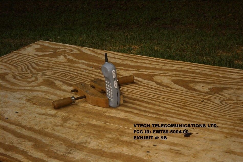
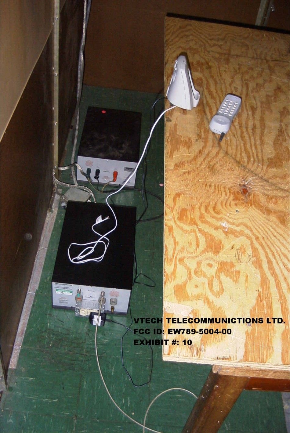
TABLE OF CONTENTS APPLICANT: VTECH TELECOMMUNICATIONS LTD. FCC ID: EW789-5004-00 TEST REPORT CONTAINING: PAGE 1.............TEST EQUIPMENT LIST AND TEST PROCEDURE PAGE 2.............TEST PROCEDURE CONTD. PAGE 3-4...........RADIATION INTERFERENCE TEST DATA PAGE 5.............POWERLINE CONDUCTED PAGE 6.............OCCUPIED BANDWIDTH EXHIBIT ATTACHMENTS: EXHIBIT 1.........FCC ID LABEL SAMPLE & SKETCH OF LOCATION EXHIBIT 2.........BLOCK DIAGRAM EXHIBIT 3A........SCHEMATIC - BASE UNI EXHIBIT 3B........SCHEMATIC - RF BOARD - BASE EXHIBIT 3C........SCHEMATIC - RF BOARD - HANDSET EXHIBIT 3D........SCHEMATIC - KEYBORAD - HANDSET EXHIBIT 4A........FRONT VIEW EXTERNAL PHOTOGRAPHS EXHIBIT 4B........REAR VIEW EXTERNAL PHOTOGRAPHS EXHIBIT 4C-4D.....COMPONENT VIEW INTERNAL PHOTOGRAPH EXHIBIT 4E-4F.....COPPER VIEW INTERNAL PHOTOGRAPH EXHIBIT 5A-5R.....INSTRUCTION MANUAL EXHIBIT 6A-6C.....CIRCUIT DESCRIPTION EXHIBIT 7A-7B.....POWERLINE CONDUCTED PLOTS EXHIBIT 8A........OCCUPIED BANDWIDTH PLOT - HIGH FREQUENCY - HD EXHIBIT 8B........OCCUPIED BANDWIDTH PLOT - 2500 Hz - BASE EXHIBIT 8C........OCCUPIED BANDWIDTH PLOT - LOW FREQUENCY - BASE EXHIBIT 8D........OCCUPIED BANDWIDTH PLOT - LOUD VOICE EXHIBIT 9A........BASE RADIATED TEST SET UP PHOTO EXHIBIT 9B........HANDSET RADIATED TEST SET UP PHOTO EXHIBIT 10........POWERLINE CONDUCTED TEST SET UP PHOTO APPLICANT: VTECH TELECOMMUNICATIONS LTD. FCC ID: EW789-5004-00 REPORT #: T:\CUS\V\VTECH\226AH0\226AH0.RPT PAGE: TABLE OF CONTENTS LIST APPLICANT: VTECH TELECOMMUNICATIONS LTD. FCC ID: EW789-5004-00 TEST EQUIPMENT LIST 1._X_Spectrum Analyzer: HP 8566B-Opt 462, S/N 3138A07786, w/ preselector HP 85685A, S/N 3221A01400, Quasi-Peak Adapter HP 8565OA, S/N 3303A01690 & Preamplifier HP 8449B-OPT H02, S/N 3008A00372 Cal. 10/17/99 2._X_Biconnical Antenna: Eaton Model 94455-1, S/N 1057 3._X_Log-Periodic Antenna: Electro-Metrics Model EM-6950, S/N 632 4._X_Double-Ridged Horn Antenna: Electro-Metrics Model RGA-180, 1-18 GHz, S/N 2319 Cal. 4/27/99 5.___Horn 40-60GHz: ATM Part #19-443-6R 6._X_Line Impedance Stabilization Network: Electro-Metrics Model ANS-25/2, S/N 2604 Cal. 2/9/00 7.___Temperature Chamber: Tenney Engineering Model TTRC, S/N 11717-7 8.___Frequency Counter: HP Model 5385A, S/N 3242A07460 Cal 10/6/99 9.___Peak Power Meter: HP Model 8900C, S/N 2131A00545 Cal 7/19/99 10._X_Open Area Test Site #1-3meters Cal. 12/22/99 11.___Signal Generator: HP 8640B, S/N 2308A21464 Cal. 9/23/99 12.___Signal Generator: HP 8614A, S/N 2015A07428 Cal. 5/29/99 13.___Passive Loop Antenna: EMCO Model 6512, 9KHz to 30MHz, S/N 9706-1211 Cal. 6/23/97 14.___Dipole Antenna Kit: Electro-Metrics Model TDA-30/1-4, S/N 153 Cal. 11/24/99 15.___AC Voltmeter: HP Model 400FL, S/N 2213A14499 Cal. 9/21/99 16.___Digital Multimeter: Fluke Model 8012A, S/N 4810047 Cal 9/21/99 17.___Digital Multimeter: Fluke Model 77, S/N 43850817 Cal 9/21/99 18.___Oscilloscope: Tektronix Model 2230, S/N 300572 Cal 9/23/99 TEST PROCEDURE GENERAL: This report shall NOT be reproduced except in full without the written approval of TIMCO ENGINEERING, INC. The UUT was transmit- ting a test signal during the testing. RADIATION INTERFERENCE: The test procedure used was ANSI STANDARD C63.4-1992 using a HEWLETT PACKARD spectrum analyzer with a prese- lector. The analyzer was calibrated in dB above a microvolt at the output of the antenna. The resolution bandwidth was 100KHz and the video bandwidth was 300KHz up to 1.0GHz and 1.0MHz with a video BW of 3.0MHz above 1.0GHz. The ambient temperature of the UUT was 74.3oF with a humidity of 69%. APPLICANT: VTECH TELECOMMUNICATIONS LTD. FCC ID: EW789-5004-00 REPORT #: T:\CUS\V\VTECH\226AH0\226AH0.RPT PAGE #: 1 APPLICANT: VTECH TELECOMMUNICATIONS LTD. FCC ID: EW789-5004-00 TEST PROCEDURES CONTINUED FORMULA OF CONVERSION FACTORS: The Field Strength at 3m was estab- lished by adding the meter reading of the spectrum analyzer (which is set to read in units of dBuV) to the antenna correction factor sup- plied by the antenna manufacturer. The antenna correction factors are stated in terms of dB. The gain of the Preselector was accounted for in the Spectrum Analyzer Meter Reading. Example: Freq (MHz) METER READING + ACF = FS 33 20 dBuV + 10.36 dB = 30.36 dBuV/m @ 3m POWER LINE CONDUCTED INTERFERENCE: The procedure used was ANSI STAN- DARD C63.4-1992 using a 50uH LISN. Both lines were observed. The bandwidth of the spectrum analyzer was 10kHz with an appro- priate sweep speed. The ambient temperature of the UUT was 74.3oF with a humidity of 69%. ANSI STANDARD C63.4-1992 10.1.7 MEASUREMENT PROCEDURES: The UUT was placed on a table 80 cm high and with dimensions of 1m by 1.5m. The UUT was placed in the center of the table (1.5m side). The table used for radiated measurements is capable of continuous rotation. When an emission was found, the table was rotated to produce the maximum signal strength. At this point, the antenna was raised and lowered from 1m to 4m. The antenna was placed in both the horizontal and vertical planes. The situation was similar for the conducted measurement except that the table did not rotate. The EUT was setup as described in ANSIC63.4-1992 with the EUT 40 cm from the vertical ground wall. APPLICANT: VTECH TELECOMMUNICATIONS LTD. FCC ID: EW789-5004-00 REPORT NO.: T:\CUS\V\VTECH\226AH0\226AH0.RPT PAGE #: 2 APPLICANT: VTECH TELECOMMUNICATIONS LTD. FCC ID: EW789-5004-00 NAME OF TEST: RADIATION INTERFERENCE RULES PART NUMBER: 15.249, 15.209 REQUIREMENTS: FIELD STRENGTH FIELD STRENGTH S15.209 of Fundamental: of Harmonics 30 - 88 MHz 40 dBuV/m @3M 902-928 MHZ 88 -216 MHz 43.5 2.4-2.4835 GHz 216 -960 MHz 46 94 dBuV/m @3m 54 dBuV/m @3m ABOVE 960 MHz 54dBuV/m EMISSIONS RADIATED OUTSIDE OF THE SPECIFIED FREQUENCY BANDS, EXCEPT FOR HARMONICS, SHALL BE ATTENUATED BY AT LEAST 50 dB BELOW THE LEVEL OF THE FUNDAMENTAL OR TO THE GENERAL RADIATED EMISSION LIMITS IN 15.209, WHICHEVER IS THE LESSER ATTENUATION. TEST RESULTS: This unit DOES meet the FCC requirements. TEST DATA: METER READING …
Text truncated - open the document above for the full version.
Contact Information
Applicant
Michael Tsui(Approbation Supervisor)
Test Firm
Timco Engineering, Inc.S Sanders
Technical Specifications
| # | Rule Parts | Frequency Range | Power Output |
|---|---|---|---|
| 2 | 15C | 926 MHz - 928 MHz | - |
Other Applications from VTech Telecommunications Ltd

EW780-2531-01
Sep 12, 2024Video Baby Monitor
Equipment Class
DSS - Part 15 Spread Spectrum Transmitter
EW780-2531-00
Sep 12, 2024Video Baby Monitor
Equipment Class
DXX - Part 15 Low Power Communication Device Transmitter
EW780-2792-00A
Sep 09, 2024Video Baby Monitor
Equipment Class
DSS - Part 15 Spread Spectrum Transmitter
EW780-H0HQ-13
Aug 20, 2024SIP cordless hotel phone
Equipment Class
PUB - Part 15 Unlicensed PCS Base Station
EW780-2365-00A
Aug 19, 2024Video Baby Monitor
Equipment Class
DSS - Part 15 Spread Spectrum Transmitter