FRWRT-138FNAirborne Transceiver 138 to 174 MHz
Wulfsberg Electronics Division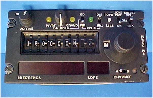
Click to zoom
Application Details
- Equipment Class
- TNB - Licensed Non-Broadcast Station Transmitter
- Date of Grant
- Oct 08, 2001
- Application Purpose
- Original Equipment
- Date of Application
- Jul 01, 2001
- Equipment Note
- Airborne Transceiver 138 to 174 MHz
- Frequency Range
- 138.00000000 - 174.00000000
- Country
- United States
Documents & Files
Document Text
Text extracted from the exhibit documents filed with the FCC. Open a document above to read the original.
Users Manual
C-1000/S OPERATOR'S MANUAL INTRODUCTION This Operator's Manual contains detailed information to assist you in the proper operation of the C-1000/S Control Head. Refer to the picture on the following page as you read the operating instructions. PURPOSE OF EQUIPMENT The C-1000/S control unit is designed for use with Wulfsberg's Flexcomm communication systems. Flexcomm provides FM communications in low band VHF, high band VHF, UHF and VHF AM. Flexcomm provides total flexibility for interagency communications. The units provide channeling capability for all the FM bands plus the air traffic control band. The C-1000/S is a fully frequency-agile control unit. It provides the ability to thumbwheel control all of the authorized Flexcomm system channels. It also provides 30 programmable preset channels. And the programming capability to change any of the preset channel frequencies is built into the control unit. This built-in operator programming capability can be disabled if the user desires. Transceivers must be used only on your specifically authorized frequencies. NOTE: The C-1000/S Control Unit has shop accessible mode of operation selector switches. The configuration of the switches alters the operation of the control and the configuration must be known to properly utilize the features of the C-1000/S. Features and capabilities of the C-1000/S that may be internally enabled/disabled are: ! THUMBWHEEL LIGHTING - normally the thumbwheels are back-lit continuously for night use but may be internally disabled. ! FREQUENCY AND TONE DISPLAY - normally the display is off except when the present RCV/XMT switch is depressed either to preset channel frequency and tone information or to re-program the channel information. The display may be configured internally for the display to be on continuously. ! GUARD CHANNEL PROGRAMMING - may be internally disabled. ! PAGE A AND B CHANNEL PROGRAMMING – may be internally disabled for page A or page B channels or both. ! MANUAL SIMPLEX CHANNEL - may be internally restricted to receive only. ! CHANNEL MEMORY DISCRETE OUTPUTS – may be shop programmed with each channel to provide control of external accessory equipment. Should the operator re-program a channel without access to the internal switches, pre-programmed channel memory discrete information may be lost. If the unit has been modified for narrow/wide band operation, memory discrete number two will not be a user- defined discrete output. DESIGN FEATURES ! The C-1000/S is designed for ease of operation, maintenance and installation. ! Channel Memory retention maintained with no power applied. Some restrictions may apply with S version installations. ! All Flexcomm control units are interchangeable within the system wiring. ! Guard channel transmit frequencies and tones. ! Five Channel Memory Discrete Outputs (four when modified for narrow band); shop programmable with each channel. ! Direct/Repeat feature. ! Integral front panel lighting. FREQUENCY SELECTION AND DISPLAY Please note that the international aircraft standard is used in the frequency selection and frequency presentation of the 0.5 kHz frequencies. That is: 154.320 reads 154.320 154.3225 reads 154.322 464.325 reads 464.325 464.3275 reads 464.327 CONTROL OPERATION The following describes the operation of each operator accessible control knob, switch or indicator: ! PRESET CHANNEL SELECTORS: Allows selection of 30 channels of pre-programmed frequencies, tones and Channel Memory Discretes. ! TEST/LOAD Switch: Disables the receiver squelch, also, when activated simultaneously with the Preset switch, loads preset frequencies, tones and five Channel Memory Discretes. ! PRESET - RCV/XMT Switch: Used in conjunction with the LOAD/TEST Switch, selects either receive or transmit half of channel memory. Activates seven segment frequency and tone LED displays. ! MAIN RECEIVER Squelch Lamp: Indicates signal on Main Receiver. Dims automatically. ! GUARD RECEIVER Squelch Lamp: Indicates signal on Guard Receiver. Dims automatically. ! ON/OFF/VOLUME Control ! TONE - ON/OFF/MNL Switch: Allows manual selection of transmitted tone by way of thumbwheel TONE selectors in MNL position, allows Main and Guard tone squelches to operate in the ON position, and allows Main and Guard receiver tone squelches to be disabled in either the MNL or OFF positions. In either the OFF or MNL positions the receiver's squelches operate via their noise squelch circuitry. ! T/R SELECT Switch -MAIN/BOTH/GUARD: In the MAIN position - enables the Main Receiver only and transmits on the main channel selected. In the BOTH position - enables both the Main and Guard Receivers and transmits on either the main or guard channel (dependent on the XMTR-MN/GD switch); in the GUARD position - enables only the Guard Receiver and transmits on the selected guard channel. ! XMTR - MN/GD Switch: Selects either main channel or guard channel during transmitter operation only if the T/R-MAIN/BOTH/GUARD switch is in the BOTH position. ! XMTR Lamp: Indicates transmitter operating, dims automatically. ! RPT/DIR Switch: Selects transmitter to operate on different frequency than receiver (RPT) or same frequency as receiver (DIR) during main channel operation. Selects one of two guard channels during guard channel transmitter operation and during guard transmit channel programming. ! FREQUENCY and TONE Selectors: Internally lighted thumbwheels used in manual selection and programming of frequencies and tones. Lighting may be disabled by means of an internal switch. ! N/W SWITCH: Selects either Narrow or Wide Band operation. When N is selected and the channel selector switch is on M, an LED lights in the lower right corner of the kHz display. The LED also lights when a preset memory channel has been programmed for narrow band. PRESET CHANNEL PROGRAMMING INSTRUCTIONS Turn the equipment On by rotating the MAIN ON/OFF volume control clockwise. Aircraft or vehicle power must be available to the unit by operating the approp…
Text truncated - open the document above for the full version.
External Photos
C-1000 Control Head for RT-138FN External Photos Control Head
External Photos
RT-138FN Front Panel External Photo Radio Front Panel
External Photos
Side View of RT-138FN Transceiver External Photo Side View
ID Label/Location Info
ID LABEL/LOCATION INFO LABEL
Internal Photos
Internal Photos Chassis
Internal Photos
Internal Photos Audio Board
Internal Photos
Internal Photos Power Supply
Internal Photos
Internal Photos Synthesizer Board
Internal Photos
Internal Photos RT Module
Internal Photos
Internal Photos Guard Receiver
Internal Photos
Internal Photos Logic Board
Operational Description
RT-138F NARROW BAND CONVERSION MAINTENANCE MANUAL ADDENDUM Manual Number 150-040893Page 2Apr 2001 Revision A Wulfsberg Electronics Division A Chelton Group Company Section 2Theory of Operation 2.1General The standard RT-138F and narrow banded RT-138F are identical except for the following items: • A Daughter board has been added to the Audio board for gain switching purposes. • One wire that is normally tied back (mem discrete #2) is now soldered to ‘Y’ on the Audio board connector A3J3. • IF filters FL1 and FL2 (20 Mhz filters) were changed to provide a steeper roll-off and narrower bandwidth. The Guard receiver will have its 16.9 MHz IF filters changed to steeper roll-off and narrower bandwidth characteristics as well. • Some parts were changed in the 4 Section 3 kHz Low Pass Filter on the Audio board to provide a narrower response. The theory of operation in this document covers only those parts of the Audio board that have been affected by the narrow band modification. The remaining operations are covered in the original Theory of Operation in the RT-138F Maintenance Manual. 2.2Operational Block Diagram Figure 2-1 is a block diagram illustrating the operation of the ‘-050’ Audio board used in the RT-138F with the narrow band Daughter board installed. 2.3Narrow Banded Audio Board Circuit Theory A3U1A, the Main Receiver inverting buffer no longer drives the main squelch circuitry in the narrow banded Audio board. The signal for the main squelch circuitry is now taken directly from pin A3P3-21 and input to the isolated leg of C4. The reason for this change is because the gain of A3U1A is now switchable to double the amplitude of the incoming audio when in the narrow band mode. Since the gain is doubled in the narrow band mode, the noise is also doubled. The squelch circuitry therefore would sense the extra noise and squelch accordingly. This would create one squelch point for narrow and a different point for wide band depending on which is selected on the C-1000 control head. By picking off the signal before it gets to A3U1A, the squelch remains consistent regardless of the gain selected for the buffer and independent of whether the incoming signal is narrow or wide band. The Guard Audio Buffers’ gain is also switchable for the purpose of doubling the amplitude of an incoming narrow band signal. The squelch circuitry however, is contained in the Guard so the signal received by the Audio board from the Guard has already been screened for squelch. A3U9B, the Modulation Summing Buffer, also has switchable gain. It’s gain however, is cut in half by the gain switch in the narrow band mode in order to keep the modulation within narrow band specs during transmit. RT-138F NARROW BAND CONVERSION MAINTENANCE MANUAL ADDENDUM Manual Number 150-040893 Page 3 Apr 2001 Revision A Wulfsberg Electronics Division A Chelton Group Company Figure 2-1. RT-138F Narrow-Band Audio Board Block Diagram RT-138F NARROW BAND CONVERSION MAINTENANCE MANUAL ADDENDUM Apr 2001Page 3Manual Number 150-040893 Revision A Wulfsberg Electronics Division A Chelton Group Company 2.3.1Narrow Band Gain Boost When the radio incorporates a narrow band system, the received audio is reduced by a factor of two due to the reduced modulation deviation. To compensate for this reduction, a times- two audio boost circuit is supplied for the Main and Guard receive audio paths and is controlled by the dNarrow Ban control signal. The Main Receiver audio is buffered by amplifier A3U1A. The gain of this stage will be 1.18 with a high signal (+10 Vdc) applied to U1X pin 1. A low signal applied to this pin will double the gain to 2.36. The Guard Receiver audio is buffered by amplifier A3U15A. This is a switchable gain stage that is unity when a high signal (+10 Vdc) is applied to U1X pin 9. A low signal applied to this pin gives it a gain of two. 2.3.2Narrow Band Gain Reduction Another aspect of a radio that incorporates a narrow band system is that when transmitting in narrow band, the modulated audio and CTCSS tone deviation are reduced by a factor of two. This reduction is created by making the Modulation Summing Buffer a switchable gain stage controlled by the narrow band control signal. The Modulation Summing Buffer A3U9B is a switchable gain stage that is unity when a high signal (+10 Vdc) is applied to U1X pin 8. A low signal applied to this pin cuts the gain in half reducing the deviation by a factor of two when in narrow band. 2.3.34 Section 3kHz Low Pass Filter The audio response needs to be shaped to fit a certain modulation response curve in the narrow band mode as well as the standard band. This is more difficult in the narrow band mode because the sidebands created by the modulated audio need to be suppressed considerably at 12.5 kHz from center whereas in the standard mode we’re concerned with 25 kHz and beyond where the sidebands are already attenuated sufficiently. The response is measured using a modulation frequency of 300 Hz to 5 kHz. Over this range, the output can’t be over-modulated or under-modulated as defined by the TIA/EIA Standard. The changes made to the 3 kHz Low Pass Filter are there to keep the modulation response within the specified limits. R108 has been reduced to increase the gain of this stage. C51 was increased to provide additional filtering and R119 was decreased to reduce the gain of the final stage of the filter. R118 was decreased primarily to affect the filter roll-off characteristics and R117 was increased mainly to affect the overall shape of the response curve.
Parts List/Tune Up Info
RT-138F NARROW BAND CONVERSION MAINTENANCE MANUAL ADDENDUM Apr 2001Page 13Manual Number 150-040893 Revision A Wulfsberg Electronics Division A Chelton Group Company Section 5Parts List 5.1General Since the complete ‘-050’ Audio board Parts List is in the RT-138F Maintenance Manual, it will not be included in this addendum. The Audio board components will remain the same except for the addition of the Daughter board and its associated components and the components changed in the 4 Section 3kHz Low Pass Filter. Wulfsberg Document Number 310-040654-01, Rev. C, Parts List, Daughter Board, RT-138F Audio Board, Narrow Bandwidth. Parts List, Daughter Board, RT-138F Audio Board, Narrow Bandwidth ItemQtyPart NumberDescriptionReference 12106-04104-0047Cap, .1uF, 50V, Chip, 1206C1-C2 21120-03393-0002IC DG441DY Quad SPST Analog Switch U1 32139-01002-0000RES 10 K Ohm 1% 1/8W ChipR1-2 41139-01003-0000RES 100 K Ohm 1% 1/8W ChipR5 51139-03322-0000RES 33.2 K Ohm 1% 1/8W ChipR4 61139-04992-0000RES 49.9 K Ohm 1% 1/8WwChipR3 7A/R600-0021-000Protective Coating 81108-640654-01P C Bd, Audio Bd NB Mod(RT-138/F) 9A/R16031-128 AWG Wire Wrap Wire 10A/R16022-2Shrink Sleeving, .063 3 kHz Low Pass Filter Modifications 11111-00001-00875600pf Capacitor 50v 5%C51 22231-1005-02110k Resistor 1%R117,118 31230-04000-224220k Resistor ¼ WattR108 41136-02672-007226.7k Resistor 1%R119 RT-138F NARROW BAND CONVERSION MAINTENANCE MANUAL ADDENDUM Manual Number 150-040893Page 14Apr 2001 Revision A Wulfsberg Electronics Division A Chelton Group Company 5.1.1The following parts will replace the IF filters to narrow band the Main receiver. ItemQtyPart NumberDescriptionReference 12139-340658-000Filter, 20 Mhz, 8 poleFL1, FL2 5.1.2The following parts will replace the IF filters to narrow band the Guard receiver. ItemQtyPart NumberDescriptionReference 12139-340683-000Filter, 16.9 Mhz, 8 poleFL1, FL2
Parts List/Tune Up Info
RT-138F NARROW BAND CONVERSION MAINTENANCE MANUAL ADDENDUM Apr 2001Page 5Manual Number 150-040893 Revision A Wulfsberg Electronics Division A Chelton Group Company Section 3Maintenance 3.1Disassembly See the RT-138F Maintenance Manual, Section 2.1. 3.2Test Equipment See the RT-138F Maintenance Manual, Section 2.2. 3.3RT-138F Overall Performance Tests See the RT-138F Maintenance Manual for wide band tests. All narrow band tests are performed with a C-1000 control head that has been modified for narrow band operation. The following tests apply to a narrow banded RT-138F and are done in the narrow band mode. 3.3.1Receiver Audio Output Using a 1000 uv signal with standard modulation, the audio output shall be typically 9.0 vrms across 600 ohms when in the narrow band mode. The test should be performed at one channel for the Main receiver and at one channel for the Guard receiver. 3.3.2Transmitter Deviation Capability With an input of .25 Vrms at 1000 Hz, the transmitter shall produce a deviation greater than 1.5 kHz. 3.3.3Transmitter Deviation Limiter A 2.5 Vrms audio input signal shall produce no greater than 2.5 kHz deviation. 3.3.4Transmitter CTCSS Selection of a tone from either a test set or a control unit shall produce a tone deviation between 350 and 475 Hz (375 Hz nominal). This test needs to be performed at only one channel. RT-138F NARROW BAND CONVERSION MAINTENANCE MANUAL ADDENDUM Manual Number 150-040893Page 6Apr 2001 Revision A Wulfsberg Electronics Division A Chelton Group Company 3.4Troubleshooting 3.4.1Audio Board Troubleshooting Procedure The supporting inputs called out in section 2.5.4 in the RT-138F Maintenance Manual, there is an additional input on the narrow banded Audio board called dNarrow Ban and the narrow banded C-1000 control unit is its source. dNarrow Ban , when pulled low, will double the gain of A3U1A and A3U15A by applying the signal to the active low inputs 1 and 9 respectively of Analog Switch U1X. U1X and its associated components are on the Daughter Board Assembly 300-040654. With the analog switch enabled, resistors R74 and R5A are effectively paralleled thus doubling the gain of Guard Audio buffer U15A. Also, R1 and R3A are paralleled causing the gain of the Main Audio buffer U1A to double. A high level on these pins would disable U1X and take R5A and R3A electrically out of the circuit. A high on the dNarrow Ban line should be approximately 10 Volt but anything over 2.4 Volt would be taken as a high by the device and a low is anything less than .8 Volt. The Modulation Summing buffer U9B is also affected by the dNarrow Ban control line. Its gain is effectively halved by paralleling resistors R4A and R66 when U1X pin 8 is low. When U1X pin 8 is high, R4A is electrically removed from the circuit and the buffer is at unity gain. 3.5Alignment Procedures Refer to the RT-138F Maintenance Manual for the alignment procedures.
Schematics
RT-138F NARROW BAND CONVERSION MAINTENANCE MANUAL ADDENDUM Manual Number 150-040893-000 Page 8 Apr 2001 Revision A Wulfsberg Electronics Division A Chelton Group Company Figure 4-1. RT-138F Narrow-Band Audio Board Schematic Diagram RT-138F NARROW BAND CONVERSION MAINTENANCE MANUAL ADDENDUM Manual Number 150-040893 Page 9 Apr 2001 Revision A Wulfsberg Electronics Division A Chelton Group Company Figure 4-1 RT-138F Narrow Band Audio Board Schematic Diagram RT-138F NARROW BAND CONVERSION MAINTENANCE MANUAL ADDENDUM Manual Number 150-040893-000 Page 10 Apr 2001 Revision A Wulfsberg Electronics Division A Chelton Group Company Figure 4-1 RT-138F Narrow-Band Audio Board Schematic Diagram RT-138F NARROW BAND CONVERSION MAINTENANCE MANUAL ADDENDUM Manual Number 150-040893 Page 11 Apr 2001 Revision A Wulfsberg Electronics Division A Chelton Group Company Figure 4-2. RT-138F Narrow-Band Chassis Schematic Diagram (Page 1 of 2) -OX SHOWN RT-138F NARROW BAND CONVERSION MAINTENANCE MANUAL ADDENDUM Manual Number 150-040893-000 Page 12 Apr 2001 Revision A Wulfsberg Electronics Division A Chelton Group Company Figure 4-2 RT-138F Narrow Band Chassis Schematic Diagram (Page 2 of 2) -5X SHOWN RT-138F NARROW BAND CONVERSION MAINTENANCE MANUAL ADDENDUM Manual Number 150-040893 Page 13 Apr 2001 Revision A Wulfsberg Electronics Division A Chelton Group Company Figure 4-3 RT-138F Narrow Band Audio Board Assembly
Test Report
ARCHIVE 1/150-040684.A.DOCPage 2 of 25 TABLE OF CONTENTS 1INTRODUCTION.............................................................................................................................. 4 2TEST FACILITIES............................................................................................................................ 4 3CERTIFICATION OF DATA ............................................................................................................. 5 4EXPOSITORY STATEMENTS; Paragraph 2.983 (a) - (d): ............................................................. 6 4.1Name of Applicant; Paragraph 2.983 (a): ........................................................................... 6 4.2Identification of Equipment; Paragraph 2.983 (b): .............................................................. 6 4.3Production Quantity; Paragraph 2.983 (c): ......................................................................... 6 4.4Types of Emission; Paragraph 2.983 (d) (1): ...................................................................... 6 4.5Frequency Range; Paragraph 2.983 (d) (2):....................................................................... 6 4.6Power Rating; Paragraph 2.983 (d) (3):.............................................................................. 6 4.7Maximum Power Rating; Paragraph 2.983 (d) (4): ............................................................. 6 4.8DC Voltage and Current into final Amplifier; Paragraph 2.983 (d) (5): ............................... 6 4.9Function of Semiconductors and other active devices; Paragraph 2.983 (d) (6):............... 6 4.10Complete Circuit Diagrams; Paragraph 2.983 (d) (7): ........................................................ 6 4.11Instruction Book; Paragraph 2.983 (d) (8):.......................................................................... 7 4.12Tune-up Procedure at Nominal Power; 2.983 (d) (9):......................................................... 7 4.13Circuitry and Devices for Determining and Stabilizing Frequency; Paragraph 2.983 (d) (10): ............................................................................................................................................ 7 4.14Circuits for Suppression of Spurious Radiation, Limiting of Modulation and Limiting of Power; Paragraph 2.983 (d) (11): ....................................................................................... 7 5TEST PROCEDURES AND CONDITIONS ..................................................................................... 7 5.1Measurement Procedures; Paragraph 2.947 (a), (b), (c):................................................... 7 5.2Test Equipment; Paragraph 2.947 (d):................................................................................ 7 5.3Test Conditions for Transmitter Type Acceptance Test:..................................................... 8 6MEASUREMENT DATA FOR TYPE ACCEPTANCE...................................................................... 8 6.1RF Power Output; Paragraph 2.985 (a): ............................................................................. 8 6.1.1Test Set-up:......................................................................................................................... 8 6.1.2Power Measurements: ........................................................................................................8 6.2Modulation Characteristics; Paragraph 2.987:.................................................................... 8 6.2.1Test setup for Frequency Response and Limiting: ............................................................. 9 6.2.2Frequency Response; Paragraph 2.987 (a) ....................................................................... 9 6.2.3Measured Frequency Response: ...................................................................................... 10 6.3Modulation Limiting Characteristics; Paragraph 2.987 (b)................................................ 10 6.3.1Modulation Limiting Test Setup......................................................................................... 11 6.3.2Measured Standard Band Limiting.................................................................................... 11 6.3.3Measured Narrow Band Limiting....................................................................................... 12 6.4Occupied Bandwidth; Paragraph 2.989: ........................................................................... 12 6.4.1Occupied Bandwidth Test Procedure; Paragraph 2.989 .................................................. 12 6.4.2Occupied Bandwidth Test Setup:...................................................................................... 13 6.4.3Measured Standard Band Occupied Bandwidth: .............................................................. 13 6.4.4Measured Narrow Band Occupied Bandwidth: ................................................................. 14 6.5Spurious Emissions; Paragraph 2.991, 2.993: ................................................................. 14 6.5.1Spurious Emissions at the Antenna Terminals; Paragraph 2.991: ................................... 14 6.5.2Spurious Emission Test Setup: ......................................................................................... 15 6.5.3Field Strength Measurement of Spurious Radiation; Paragraph 2.993 ............................ 15 6.6Frequency Stability; Paragraph 2.995:.............................................................................. 15 6.6.1Test Setup for Frequency Stability: ................................................................................... 15 6.6.2Temperature; Paragraph 2.995 (a) and (b):...................................................................... 16 6.6.3Measured Temperature Data: ........................................................................................... 16 6.6.4Frequency Stability Under Voltage Variation; Paragraph 2.995 (d).............................…
Text truncated - open the document above for the full version.
Test Report
ARCHIVE 1/150-040887.A.DOCPage 1 of 16 APPLICATIONREVISIONS REV A NEXT ASSEMBLYFINAL ASSEMBLYREVDESCRIPTIONDATEAPPROVED A INITIAL RELEASE PER DCN W1573 7/3/01 V. Wallace SH 1 DWG. NO . 150-040887 THIS DOCUMENT CONTAINS PROPRIETARY INFORMATION OF WULFSBERG ELECTRONICS DIVISION, A CHELTON GROUP COMPANY. NEITHER RECEIPT NOR POSSESSION THEREOF CONFERS ANY RIGHT TO REPRODUCE, OR USE, OR DISCLOSE, IN WHOLE OR IN PART, ANY SUCH INFORMATION WITHOUT WRITTEN AUTHORIZATION FROM WULFSBERG ELECTRONICS DIVISION. APPROVALSDATE DRAWN R. DeLong 7/3/01 TITLE: TYPE ACCEPTANCE REPORT MODEL RT-138FN FCC ID: FRWRT-138FN CHECKED D. Ellis 7/3/01 ENGINEER R. DeLong 7/3/01 SIZE A CAGE CODE 1B7G3 DWG. NO. 150-040887 REV A ISSUED V. Wallace 7/3/01SCALE NONE ARCHIVE 1/150-040684.A.DOCPage 2 of 16 TABLE OF CONTENTS 1INTRODUCTION .............................................................................................................................. 3 2TEST FACILITIES ............................................................................................................................ 3 3CERTIFICATION OF DATA ............................................................................................................. 4 4EXPOSITORY STATEMENTS; Paragraph 2.983 (a) - (d):.............................................................. 5 4.1Name of Applicant; Paragraph 2.983 (a):............................................................................ 5 4.2Identification of Equipment; Paragraph 2.983 (b):............................................................... 5 4.3Production Quantity; Paragraph 2.983 (c):.......................................................................... 5 4.4Types of Emission; Paragraph 2.983 (d) (1): ...................................................................... 5 4.5Frequency Range; Paragraph 2.983 (d) (2): ....................................................................... 5 4.6Power Rating; Paragraph 2.983 (d) (3): .............................................................................. 5 4.7Maximum Power Rating; Paragraph 2.983 (d) (4): ............................................................. 5 4.8DC Voltage and Current into final Amplifier; Paragraph 2.983 (d) (5):................................ 5 4.9Function of Semiconductors and other active devices; Paragraph 2.983 (d) (6): ............... 5 4.10Complete Circuit Diagrams; Paragraph 2.983 (d) (7):......................................................... 5 4.11Instruction Book; Paragraph 2.983 (d) (8): .......................................................................... 6 4.12Tune-up Procedure at Nominal Power; 2.983 (d) (9): ......................................................... 6 4.13Circuitry and Devices for Determining and Stabilizing Frequency; Paragraph 2.983 (d) (10): ............................................................................................................................................. 6 4.14Circuits for Suppression of Spurious Radiation, Limiting of Modulation and Limiting of Power; Paragraph 2.983 (d) (11):........................................................................................ 6 5TEST PROCEDURES AND CONDITIONS...................................................................................... 6 5.1Measurement Procedures; Paragraph 2.947 (a), (b), (c): ................................................... 6 5.2Test Equipment; Paragraph 2.947 (d): ................................................................................ 6 5.3Test Conditions for Transmitter Type Acceptance Test: ..................................................... 7 6MEASUREMENT DATA FOR TYPE ACCEPTANCE ...................................................................... 7 6.1RF Power Output; Paragraph 2.985 (a): ............................................................................. 7 6.1.1Test Set-up: ......................................................................................................................... 7 6.1.2Power Measurements: ........................................................................................................7 6.2Modulation Characteristics; Paragraph 2.987: .................................................................... 7 6.2.1Test setup for Frequency Response and Limiting:.............................................................. 8 6.2.2Frequency Response; Paragraph 2.987 (a) ........................................................................ 8 6.2.3Measured Frequency Response: ........................................................................................ 9 6.3Modulation Limiting Characteristics; Paragraph 2.987 (b) .................................................. 9 Modulation Limiting Test Setup ...................................................................................................... 10 6.3.2Measured Standard Band Limiting .................................................................................... 10 6.3.3Measured Narrow Band Limiting ....................................................................................... 11 6.4Occupied Bandwidth; Paragraph 2.989: ........................................................................... 11 6.4.1Occupied Bandwidth Test Procedure; Paragraph 2.989................................................... 11 6.4.2Occupied Bandwidth Test Setup: ...................................................................................... 12 6.4.3Measured Standard Band Occupied Bandwidth: .............................................................. 12 6.4.4Measured Narrow Band Occupied Bandwidth: ................................................................. 13 6.5Spurious Emissions; Paragraph 2.991, 2.993: .................................................................. 13 6.5.1Spurious Emission…
Text truncated - open the document above for the full version.
Contact Information
Applicant
James F Buehring(Certification Manager)
Technical Contact
Wulfsberg Electronics DivisionRobert K DeLong
[email protected]1-928-708-1501
6400 Wilkinson Drive · Prescott, Arizona · United States
Non-Technical Contact
Wulfsberg Electronics DivisionRobert K DeLong
[email protected]1-928-708-1501
Technical Specifications
| # | Rule Parts | Frequency Range | Power Output | Emission | Tolerance |
|---|---|---|---|---|---|
| 2 | 22,90.21 | 138 MHz - 174 MHz | 10 W | 11K2F3E | 2.5 ppm |
Other Applications from Wulfsberg Electronics Division
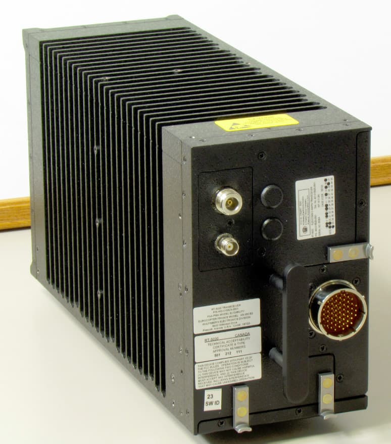
FRWRT-5000P-03
Dec 28, 201229.7 to 960 MHz Tactical Airborne Transceiver
Equipment Class
TNB - Licensed Non-Broadcast Station Transmitter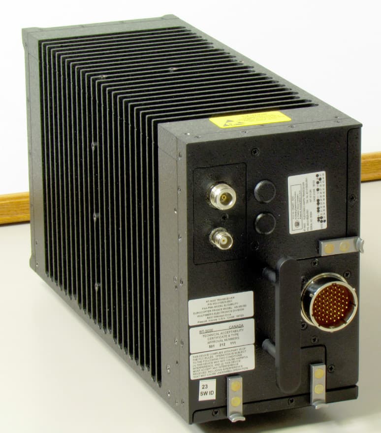
FRWRT-5000P-06
Dec 28, 201229.7 to 960 MHz Tactical Airborne Transceiver
Equipment Class
TNB - Licensed Non-Broadcast Station Transmitter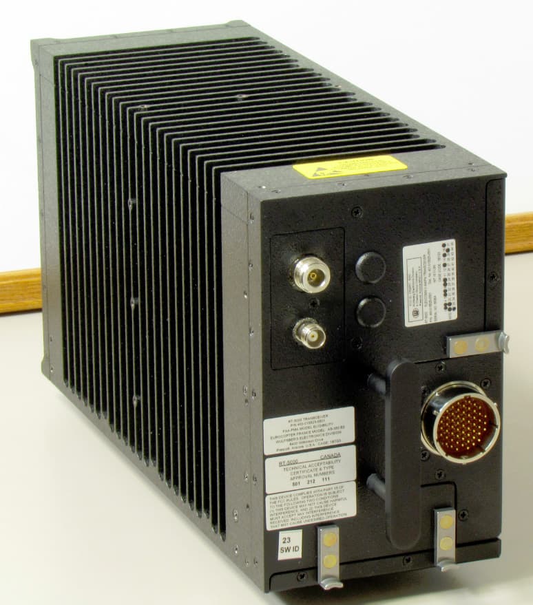
FRWRT-5000P-04
Dec 28, 201229.7 to 960 MHz Tactical Airborne Transceiver
Equipment Class
TNB - Licensed Non-Broadcast Station Transmitter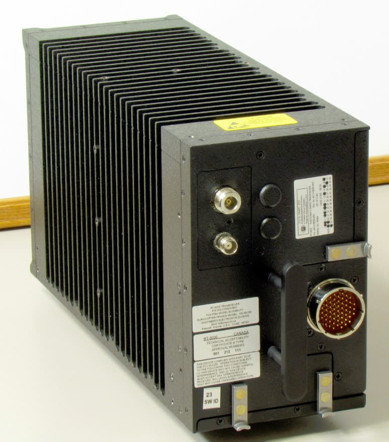
FRWRT-5000P-05
Dec 28, 201229.7 to 960 MHz Tactical Airborne Transceiver
Equipment Class
TNB - Licensed Non-Broadcast Station Transmitter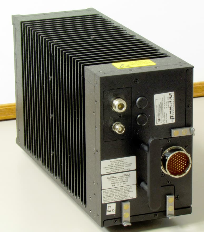
FRWRT-5000P-08
Dec 27, 201229.7 to 960 MHz Tactical Airborne Transceiver
Equipment Class
TNB - Licensed Non-Broadcast Station Transmitter