FRWVC-401BVHF ATC Communication Transceiver for aircraft ins
Wulfsberg Electronics Division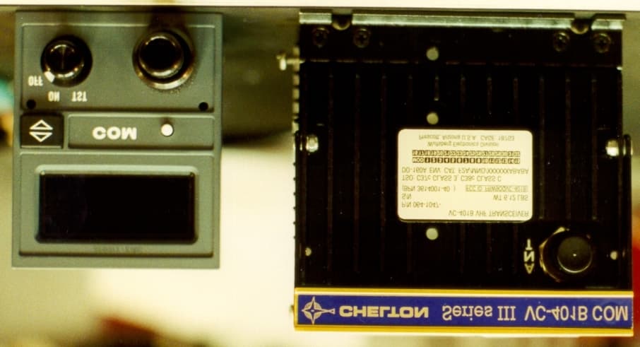
Click to zoom
Application Details
- Equipment Class
- TNB - Licensed Non-Broadcast Station Transmitter
- Date of Grant
- Jun 18, 2000
- Application Purpose
- Original Equipment
- Date of Application
- Feb 23, 2000
- Equipment Note
- VHF ATC Communication Transceiver for aircraft ins
- Frequency Range
- 118.00000000 - 152.00000000
- Country
- United States
Documents & Files
Document Text
Text extracted from the exhibit documents filed with the FCC. Open a document above to read the original.
Users Manual
Publication No. 150-040564 Rev. AJanuary 2000 Chelton Avionics Inc. A Chelton Group Company 6400 Wilkinson Drive Prescott, AZ 86305 U.S.A. Series III Avionics Pilot's Guide Series III Avionics Pilot's Guide Page ii Wulfsberg Electronics Division, located in Prescott, Arizona, designs and manufactures the Chelton Series III line of products, including the VCS-40A VHF Communications System. For more than 25 years, Wulfsberg Electronics has distinguished itself by providing top quality avionics products for civil, air transport, and military applications. Information in this manual is subject to change without notice. No part of this manual may be reproduced or transmitted in any form or by any means, electronic or mechanical, without express written permission of Chelton Avionics, Inc. Chelton Avionics, Inc. makes no warranty, expressed or implied, with regard to this manual, including but not limited to any implied warranties of merchantability, fitness for a particular purpose, and non- infringement. In addition, Chelton Avionics, Inc. makes no warranty with regard to the documentation or data contained herein. Chelton Avionics, Inc. is not liable in the event of incidental, special, consequential, or any other damages in connection with or arising from furnishing, performance, or use of this manual. 2000 Chelton Avionics, Inc. All rights reserved VCS-40A, VC-401B, CD-402B, VNS-41A, VN-411B, CD-412B, CD-413B, TRS-42A, TR-421B, CD-422B, DFS-43A, DF-431B, CD-432B, DMS-44A, DM-441B, and SD-442B are trademarks of Chelton Avionics, Inc. Series III Avionics Pilot's Guide Page iii VCS-40A VHF Communications System...................................................................................................................1 General Description................................................................................................................................................1 CD-402B Control Display Unit..............................................................................................................................2 CD-402B Controls (Fixed Channel Spacing).........................................................................................................3 CD-402B Controls (Switchable Channel Spacing).................................................................................................3 CD-402B Controls (All).........................................................................................................................................4 CD-402B Display...................................................................................................................................................5 Operating the VCS-40A.........................................................................................................................................6 VCS-40A Notes......................................................................................................................................................8 VCS-40A System Block Diagram (Typical)..........................................................................................................9 VNS-41A VHF Navigation System...........................................................................................................................10 General Description..............................................................................................................................................10 CD-412B Control Display Unit............................................................................................................................11 VNS-41A Controls...............................................................................................................................................12 VNS-41A Display.................................................................................................................................................13 Operating the VNS-41A.......................................................................................................................................15 VNS-41A Notes....................................................................................................................................................16 VNS-41A System Block Diagram (Typical)........................................................................................................17 TRS-42A ATC Transponder System........................................................................................................................18 General Description..............................................................................................................................................18 CD-422B Control Display Unit............................................................................................................................19 TRS-42A Controls................................................................................................................................................20 CD-422B Display.................................................................................................................................................23 Operating the TRS-42A........................................................................................................................................25 TRS-42A Notes....................................................................................................................................................26 TRS-42A System Block Diagram (Typical).........................................................................................................27 DFS-43A Automatic Direction Finder System........................................................................................................28 General Description.........................................................................................................................................…
Text truncated - open the document above for the full version.
External Photos
WULFSBERG ELECTRONICS DIVISION 150-040565 REV A SHEET 1 OF 25 ARCHIVE 1/150-040565.A.doc 02/25/00 9:20 AM 1 PHOTOGRAPHS OF EQUIPMENT:1.1 Typical VC-401B Transceiver and CD-402B Control head.
ID Label/Location Info
WULFSBERG ELECTRONICS DIVISION 150-040565 REV A SHEET 1 OF 25 ARCHIVE 1/150-040565.A.doc02/25/00 9:15 AM 1 EQUIPMENT IDENTIFICATION LABELS: THIS DEVICE COMPLIES WITH PART 15 OF THE FCC RULES. OPERATION IS SUBJECT TO THE CONDITION THAT THIS DEVICE DOES NOT CAUSE HARMFUL INTERFERENCE. FCC ID: FRWVC-401B VC-401B VHF TRANSCEIVER TSO: C37c CLASS 3&5, C38c CLASS C&E (BPN 3614001-40 ) P/N 064-1047- THIS RADIO IS 8.33 kHz CAPABLE S/N DO-160C ENV. CAT. WT 5.7 LBS F2XBA(MNY)XXXXXXABABATAXXX WULFSBERG ELECTRONICS DIVISION 150-040565 REV A SHEET 2 OF 25 ARCHIVE 1/150-040565.A.doc 02/25/00 9:15 AM
Internal Photos
WULFSBERG ELECTRONICS DIVISION 150-040565 REV A SHEET 1 OF 25 ARCHIVE 1/150-040565.A.doc 04/11/01 12:22 PM 1.1 Synthesizer and Receiver board. Only three surface mount resistors are mounted on the backside. They act as heating elements for the TCXO chamber. This photo is taken with eight shield covers removed to show parts. The shield walls are visible. WULFSBERG ELECTRONICS DIVISION 150-040565 REV A SHEET 2 OF 25 ARCHIVE 1/150-040565.A.doc 04/11/01 12:22 PM 1.2 Audio and Microcontroller Board No parts are on the backside of this board. Photo taken with center shield cover removed. WULFSBERG ELECTRONICS DIVISION 150-040565 REV A SHEET 3 OF 25 ARCHIVE 1/150-040565.A.doc 04/11/01 12:22 PM 1.3 H & L Interconnect Board Front and backsides are shown. WULFSBERG ELECTRONICS DIVISION 150-040565 REV A SHEET 4 OF 25 ARCHIVE 1/150-040565.A.doc 04/11/01 12:22 PM 1.4 Power Amplifier Board. No parts are located on the backside of this board. This board is directly mounted to the heat sink, which forms part of the o utside cover. This board has one shield cover, which is removed for this picture. WULFSBERG ELECTRONICS DIVISION 150-040565 REV A SHEET 5 OF 25 ARCHIVE 1/150-040565.A.doc 04/11/01 12:22 PM 1.5 Power Supply Board. No parts are located on the backside of this board.
Operational Description
VCS-40A VHF COMMUNICATION SYSTEM MAINTENANCE MANUAL Page 6-1 Section 6 – CD-402B Control Display Unit Theory Of Operation Jan 2000 SECTION 6 – CD-402B CONTROL DISPLAY UNIT THEORY OF OPERATION 1.General The CD-402B Control Display Unit establishes and displays the operating status of all VC-401B VHF Communications Transceiver functions (refer to Figure 6-1). Depending upon function selector switch position, the CD-402B function selector deactivates, activates or tests the operation of the receiver. As the VC-401B becomes activated, it sends display data to the CD-402B. The display data information consists of the last active and standby frequencies input to the VC-401B, system number and transmit annunciator. The system which is controlled by the CD-402B is displayed as system number "1", "2" or "(Blank)". A blank system number display indicates system number 3 or zero. Transmit annunciation (Tx) is displayed each time the push-to-talk switch is pressed and an RF output is present. Two system errors can also be annunciated on the display: FAIL1 – Synthesizer not locked, and FAIL2 – No transmitter power indication. The CD-402B provides frequency selection (Gray Code) to the VC-401B for selecting the desired operating frequency. The CD-402B provides a transfer function for swapping the active frequency and standby frequencies the VC-401B, which in turn supplies new display data information back to the CD-402B for display. Figure 6-1. Typical VCS-40A Communications System Configuration VCS-40A VHF COMMUNICATION SYSTEM MAINTENANCE MANUAL Page 6-2 Section 6 – CD-402B Control Display Unit Theory Of Operation Jan 2000 The VC-401B supplies audio to the CD-402B volume control for setting the VC-401B audio output to a desired audio output level for direct headphone or speaker use. The CD-402B receives its power from the +10 Volt DC input from the VC-401B power supply. Power for the panel lamps and the display lamps that backlight the display is received from external aircraft dimmer controls. 2.General Circuit Theory Refer to figure 6-2 for the following discussion. A. Front Panel Controls The CD-402B Control Display Unit front panel controls establish the operating status of the transceiver. The function selector switch is used to select one of three operating modes: OFF, 25, or 8.33. The function switch supplies a low level output to activate the specific operating mode in the VC-401B Audio/CPU module microprocessor. In the OFF position, the VC-401B is turned off. In the 25 position, the VC-401B is turned on with only the 25 kHz channel tuning enabled. In the 8.33 position, the VC-401B is turned on with both the 25kHz and the 8.33 kHz channel tuning enabled. Figure 6-2. Control Display Block Diagram VCS-40A VHF COMMUNICATION SYSTEM MAINTENANCE MANUAL Page 6-3 Section 6 – CD-402B Control Display Unit Theory Of Operation Jan 2000 The CD-402B volume control receives the VC-401B audio output and adjusts it to a desired audio output level for direct headphone or speaker amplifier use. The Test pushbutton applies a ground potential (TST) to the VC-401B audio/CPU module to inhibit the audio module automatic squelch circuit and permit receiver noise to be heard. This enables the operator to verify the receiver is operational. The frequency transfer pushbutton switch applies a low level output to the VC-401B CPU module microprocessor. The duration of the low level output determines the action to be taken by the microprocessor: frequency transfer, active frequency tuning, or emergency communications frequency tuning (121.500). • A momentary low level output interchanges the active and standby frequencies. Another momentary low level output reverts the active and standby frequencies back to their original state. • A low level output of two to three seconds duration causes the standby frequency to disappear and allows tuning of the active frequency instead of the standby frequency as normal. • Another two to three second low level output restores the standby frequency display and the standby frequency tuning. • In the event of a total display failure, pressing and holding the frequency transfer pushbutton for seven seconds causes the VC-401B to retune to an active frequency of 121.500 MHz. Knowing that the VC-401B is tuned to 121.500 MHz, a new frequency can be tuned by counting the number of detent stops as the frequency selector knobs are rotated. The two concentric frequency selector switches are used to select the desired communications frequency. During rotation, the microprocessor detects the logic input to the VC-401B. The frequency is then incremented or decremented by the appropriate amount. The detected frequency is then routed from the VC-401B CPU module back to the CD-402B and displayed. The large frequency knob increments (clockwise rotation) or decrements (counter-clockwise rotation) the frequency being tuned by one MHz for every detent stop. The small frequency knob increments (clockwise rotation) or decrements (counter-clockwise rotation) the frequency being tuned by 25 kHz for every detent stop when the function selector switch is in the 25 position. If the function selector switch is in the 8.33 position, the small frequency knob sequences through a list of both 25 kHz and 8.33 kHz channels (see Table 6-1). B. Display Drivers The processor in the VC-401B outputs a serial data word, clock pulse, and an enable signal which is applied to the display control module line receivers and then to the display drivers contained within the CD-402B LCD module. C. Displays The multi-segment display contains a contact on the edge of the module leading to each liquid crystal segment. A segment is activated or darkened by a voltage applied to a contact from the display driver. The individual segments are arranged to form the desired characters (annunciators, numbers, or letters) when the appropriate combinations of segments are activated. VCS-40A VHF COMMUNICATION SYSTEM MAINTENANCE MANUAL Page 6-4 Section …
Text truncated - open the document above for the full version.
Parts List/Tune Up Info
VCS-40A VHF COMMUNICATION SYSTEM MAINTENANCE MANUAL Page 5-1 Section 5 - VC-401B Illustrated Parts List Jan 2000 SECTION 5 – VC-401B VHF COMMUNICATIONS TRANSCEIVER ILLUSTRATED PARTS LISTS 1.General This section contains parts lists for the VC-401B assembly and for each of its modules. The parts list for each module is accompanied by an assembly drawing that shows the location of each component in the list. VCS-40A VHF COMMUNICATION SYSTEM MAINTENANCE MANUAL Page 5-2 Section 5 - VC-401B Illustrated Parts List Jan 2000 2.VC-401B (8.33 kHz) Top Assembly Parts List ItemQtyUMPartTitleReference 11EA400-040548-01FINAL ASSEMBLY, XCVR VC-401B 21EA090-00733-0000COVER, DUST 31EA057-03511-0001ESD DECAL CAUTION 41EA030-01260-0000DUST COVER, CONN. 5RFRF100-040589MPS VC-401B 6RFRF150-240590MASTER ROUTING VC-401B 71EAS/N TAG VC-401B 81EAFCC PART 15 TAG 91EATAMPERPROOF LABEL VCS-40A VHF COMMUNICATION SYSTEM MAINTENANCE MANUAL Page 5-3 Section 5 - VC-401B Illustrated Parts List Jan 2000 3.VC-401B (8.33 kHz) Final Assembly Parts List ItemQtyUMPartTitleReference 1RFRF300-040548-01FINAL ASSEMBLY, VC-401B TRANSCEIVER 2EA200-04210-0000PARTS LIST, CHASSIS WELD VC-401 3EA300-040463-01ASSEMBLY, VC-401B H&L INTERCONNECT BOARD 4EA300-040222-01ASSEMBLY, SYNTHESIZER/RECEIVER BOARD (VC-401B) 5EA300-040458-01ASSEMBLY, PWR SUPPLY VC-401B 6EA300-040444-01ASSY, VC-401B POWER AMPLIFIER 7EA300-040452-01CKT BD ASSY AUDIO BOARD, VC-401B 82EA090-00716-0002STANDOFF HINGED 91EA019-02565-0000INDUCTOR 1.5MHL14 101EA123-140593-01CABLE ASSEMBLY, COAX (VC-401B) 23" 111EA123-140593-02CABLE ASSEMBLY, COAX (VC-401B) 8.4" 121EA123-140594-01CABLE ASSEMBLY, BNC (VC-401B) 23" 13EA124-040526-01RIBBON CABLE ASSEMBLY (14 POSITION) 14EA124-040527-01RIBBON CABLE ASSEMBLY (20 POSITION) 15EA124-040528-01RIBBON CABLE ASSEMBLY (26 POSITION) 16EA124-040529-01RIBBON CABLE ASSEMBLY (60 POSITION) 17EA047-07760-0001CONNECTOR MTG BOX ASSY 18EA047-07759-0001PARTS LIST, CONNECTOR BOX COVER ASSY 19EA047-07996-0001PARTS LIST, FRAME, L.S. 20EA047-07767-0000PLATE 21EA047-08004-0010DUST COVER 22EA075-05054-0002HEAT SINK VC-401 23EA090-00725-0024FINGER CNT STRIP 242EAMS35649-224BNUT HEX 4-40 2520EAMS51957-13SCREW 4-40 X 1/4 PHP 264EAMS51957-3SCREW 2-56 X 1/4 PHP 277EAMS24693-3BSCREW 4-40 X 5/8 FHP BLK 286EAMS24693-C2SCREW 4-40 X 1/4 FHP 294EAMS51957-14SCREW 4-40 X 5/16 PHP 303EA089-07134-0008SCREW BHP 4-40 X .500 313EA089-06159-0004SCREW FHP 2-56 X 1/4 324EA089-07134-0004SCREW BHP 4-40 X .250 338EA089-07134-0005SCREW BHP 4-40 X .312 344EA089-07134-0006SCREW BHP 4-40 X .375 352EA089-08003-0034WASHER SPLT LK #4 3612EA089-08502-0000WASHER SPLIT LK .120 3715EA089-08507-0006WASHER FLAT SS .125 VCS-40A VHF COMMUNICATION SYSTEM MAINTENANCE MANUAL Page 5-4 Section 5 - VC-401B Illustrated Parts List Jan 2000 ItemQtyUMPartTitleReference 382EA091-00471-0000GROMMET NYLON CONT 391EA091-00471-0002GROMMET NYLON CONT 40ARAR16012-3LOCTITE ACCELERATOR & BONDER 414EA013-00050-0009BEAD FERRITE 42ARAR16022-6SLEEVING SHRINK .187 VCS-40A VHF COMMUNICATION SYSTEM MAINTENANCE MANUAL Page 5-5 Section 5 - VC-401B Illustrated Parts List Jan 2000 4.VC-401B (8.33 kHz) Receiver/Synthesizer Module Parts List ItemQtyUMPartTitleReference 11EA108-640222-01PWB, SYNTHESIZER/RECEIVER BOARD (VC-401B) 27EA112-040469-220BEAD, FERRITE 0603 SMDB521 B522 B523 6524 B525 B526 B527 36EA112-014328-01BEAD, FERRITE, SMALL (SMD)B528 B529 B530 B531 B532 B533 41EA210-040136-183CAPACITOR .018UF 10% 50V LOW DISTORTION 1206 C106 53EA210-040019-103CAPACITOR .01 UF 10% 50V X7R 0603C320 C322 C436 612EA106-04103-0047CAPACITOR .01UF 10% 50V X7R 1206C300 C309 C310 C333 C400 C401 C402 C407 C411 C412 C417 C422 72EA106-04333-0047CAPACITOR .033PF 10% 50V X7R 1206C1 10 C142 848EA210-040021-104CAPACITOR 0.1 uF 10% 50V X7R 0805C100 C101 C122 C123 C125 C126 C127 C128 C129 C134 C135 C136 C137 C143 C144 C145 C147 C148 C149 C151 C153 C155 C326 C329 C330 C331 C332 C342 C447 C448 C449 C450 C452 C453 C458 C465 C466 C467 C506 C507 C508 C509 C513 C515 C517 C525 C528 C543 99EA106-04104-0047CAPACITOR 0.1 UF 10% 50V X7R 1206C102 C108 C109 C152 C154 C156 C328 C440 C468 103EA096-01186-0024CAPACITOR 0.1UF 35V 10% CHIP TANTC120 C177 C519 111EA210-040018-0R5CAPACITOR 0.5PF 5% 50V COG 0603C314 129EA096-01186-0080CAPACITOR 1.0uF 35V 20% CHIP TANTC104 C446 C469 C516 C518 C524 C531 C542 C544 131EA210-014281 -1R5CAPACITOR 1.5PF 50V CHIP 1206C146 1410EA210-040021-103CAPACITOR 10000PF 10% 50V X7R 0805C426 C427 C428 C429 C430 C431 C432 C437 C457 C456 1515EA210-040019-102CAPACITOR 1000PF 10% 50V X7R 0603C301 C302 C303 C304 C305 C343 C344 C434 C435 C441 C459 C461 C501 C510 C511 1615EA106-04102-0016CAPACITOR 1000PF 5% 50V NPO 1206C111 C138 C140 C141 C312 C313 C315 C316 C341 C439 C463 C324 C424 C442 C443 174EA210-040019-101CAPACITOR 100PF 10% 50V X7R 0603C502 C503 C504 C505 187EA210-040018-100CAPACITOR 10PF 5% 50V COG 0603C334 C444 C445 C451 C464 C336 C338 191EA210-040018-121CAPACITOR 120PF 5% 50V COG 0603C319 201EA210-040018-120CAPACITOR 12PF 5% 50V COG 0603C335 211EA106-04120-0016CAPACITOR 12PF 5% 50V NPO 1206C116 222EA210-040018-150CAPACITOR 15PF 5% 50V COG 0603C130 C131 232EA096-01186-0087CAPACITOR 15UF 35V 10% CHIP TANTC529 C533 241EA210-014281-180CAPACITOR 18PF 50V CHIP 1206C117 VCS-40A VHF COMMUNICATION SYSTEM MAINTENANCE MANUAL Page 5-6 Section 5 - VC-401B Illustrated Parts List Jan 2000 ItemQtyUMPartTitleReference 253EA210-014281-2R4CAPACITOR 2.4PF 50V CHIP 1206C405 C406 C408 262EA210-040018-221CAPACITOR 220PF 5% 50V COG 0603C132 C103 273EA106-04221-0016CAPACITOR 220PF 5% 50V NPO 1206C121 C124 C150 284EA210-014281-220CAPACITOR 22PF 50V CHIP 1206C403 C41 0 C414 C420 296EA096-01186-0019CAPACITOR 22UF 20V 10% CHIP TANTC133 C433 C438 C514 C521 C540 304EA210-014281-270CAPACITOR 27PF 50V CHIP 1206C415 C416 C418 C419 313EA210-014281-3R3CAPACITOR 3.3pF 50V CHIP 1206C308 C311 C318 32EA210-014281-331CAPACITOR 330PF 50V CHIP 1206C325 33EA210-014281-4R7CAPACITOR 4.7PF 50V CHIP 1206C425 344EA210-040018-471CAPACITOR 470PF 5% 50V COG 0603C512 C520 C527 C538 351EA21…
Text truncated - open the document above for the full version.
Parts List/Tune Up Info
VCS-40A VHF COMMUNICATION SYSTEM MAINTENANCE MANUAL Page 3-1 Section 3 - VC-401B Alignment Procedures Jan 2000 SECTION 3 – VC-401B ALIGNMENT PROCEDURES 1.Introduction This section contains alignment procedures for VC-401B Receiver and Audio/CPU Modules. 2.VC-401B Receiver Alignment Procedure A.General The Receiver Assembly receives and processes RF signals in the frequency range of 118.000 MHz to 151.975 MHz in 25 kHz or 8.33 kHz increments. These tests are based on the tests outlined in RTCA Document RTCA/DO186A. All input RF signals are “hard” microvolts. Ensure a 6 dB 50 ohm pad is installed on the output of the signal generator. Input levels specified in this procedure already take into account the 6 dB pad. B.Instrumentation Test Equipment Required or Equivalent Test Fixture:Chelton TBD RF Signal Generator:HP 8640B (with internal audio generator) DVM:Fluke 8000A (Readout to .001) Oscilloscope:TEK 465B Audio Analyzer:HP8903B 6 dB Pad:MDS1110B-6 RF Power Meter:8901B Mod Analyzer (power meter function) RF Frequency Counter:8901B Mod Analyzer (frequency counter function) C.Alignment Procedure The unit under test must contain a visual indication that it has satisfactorily met all previous test and inspection requirements before being tested per under specification. All test equipment used must have an in-date calibration sticker. (1)Setup (a)Install the unit under test (UUT) on to the Receiver Test Fixture. Insure that the Power ON/OFF switch is in the OFF position. (b)Connect the power and control signal ribbon jumper from the Receiver Test Fixture to P2 of the UUT. (c)Set up the general test configuration as shown in Figure 3-1. (d)Center potentiometer R143 (TCXO Frequency Adjustment). VCS-40A VHF COMMUNICATION SYSTEM MAINTENANCE MANUAL Page 3-2 Section 3 - VC-401B Alignment Procedures Jan 2000 Figure 3-1. General Receiver Test Configuration (e)Remove R448 and connect power supply to TP 400. Set supply for 11 Volts. (f)Remove R441 and connect power supply to TP 420. Set supply for 1.5 Volts. NOTE:This is for the X8 version of the receiver only. Full production will have potentiometers in place of the Select-in-test resistors, R475:R448 and R464:R441. (2)Pre-alignment (a)Connect J2 (Transmitter Local Oscillator) to a frequency counter’s 50 ohm input. The expected output level is approximately 9 dBm. Use the appropriate size attenuator pad in- line with the counter. (b)Set the Receiver Test Fixture Controls as follows: ModeTX TX InterlockDisable Frequency148.000 PowerON VCS-40A VHF COMMUNICATION SYSTEM MAINTENANCE MANUAL Page 3-3 Section 3 - VC-401B Alignment Procedures Jan 2000 (c)Verify the frequency counter is showing a signal present around 148 MHz +/- 375 Hz. (d)Set the Receiver Test Fixture TX Interlock Mode to RX. (e)Verify that the 28 Volt current from the input power supply is < 400 mA. (f)Measure the voltage at TP314 (Pre-selector control voltage). Adjust the varactor trim potentiometers for 9/10 of the measured voltage at TP314: (.9 x 12.346 = 11.11 Volts) Test PointPot 308R312 304R311 305R314 309R313 (g)Center the cores in inductors L303, L305, L307 and L309. (3)VCO Alignment (a)Set the frequency for 174 MHz on the Receiver Test Set. Select TX/RX switch to TX. Observe the frequency indicated on the frequency counter. (b)Adjust R143 until the counter reads 174.000 MHz +/- 100 Hz. (c)Verify the lock detect LED CR108 is not lit. (4)Pre-Selector Alignment (a)Place covers on the pre-selectors. (b)Connect a voltmeter with 3 decimal place readout to TP413 (AUDIO OUT OF THE TEST BOX) (Primary AGC voltage). Note this AGC output can be accessed at the AGC test points on the test fixture. (c)Set the Receiver Test Set Mode TX/RX to RX. (d)Connect a signal generator to J301. Set the generator for 148 MHz with 1000 Hz 30% AM modulation. (e)Set the generator signal level for –100 dBm. Increase the signal level until the AGC voltage starts to increase. The voltage should be in the range of 5.0 volts. (f)Adjust L303, L305, L307 and L309 to increase the AGC voltage. Verify the voltage present at TP413 (AGC OUT OF THE TEST BOX). NOTE:The delayed AGC voltage is > 8 volts. If the voltage is < 8 volts, decrease the signal generator level. (g)Set the Receiver Test Set Frequency to 118.000. Set the signal generator to 118.0 MHz. VCS-40A VHF COMMUNICATION SYSTEM MAINTENANCE MANUAL Page 3-4 Section 3 - VC-401B Alignment Procedures Jan 2000 (h)Observe the AGC voltage on TP413 (AUDIO OUT OF THE TEST BOX). Adjust R311, R312, R313 and R314 to peak the AGC voltage at 118 MHz. (Make small adjustments. If an adjustment has no effect, set the pot back to its original position and go on the next adjustment.) (5)IF Alignment (a)Set the signal generator for 118 MHz AM modulated 30% with 1000 Hz. (b)Observe the AGC voltage at TP413 (AUDIO OUT OF THE TEST BOX). Adjust the IF transformers (T401, T402 and T403) to peak the AGC voltage. (c)Observe the AGC voltage at TP413 (AUDIO OUT OF THE TEST BOX). Adjust capacitors C409 and C404 to peak the AGC voltage. (6)AGC Alignment (a)Set the signal generator for 118 MHz AM modulated 30% with 1000 Hz. (b)Connect Oscilloscope unfiltered Audio Out of the Test fixture. Observe the 1000 Hz sine wave displayed on the Oscilloscope. (c)Increase the RF input level on the signal generator until the displayed signal is no longer noisy. This should be around –80 dBm. (d)Adjust the power supply connected to TP 420 until the sinewave is I volt P-P +/- .1 Volts. Measure and record this AGC Reference voltage (between 1 and 2 volts). (e)Set up the modulation analyzer to indicate SINAD in dB. Adjust the signal generator RF level until the SINAD is around 22 dB. (f)Observe the delayed AGC voltage present at TP 413 with a DVM. The reading should be between 8 and 10 volts DC. (g)Adjust the power supply until the voltage on the DVM reaches it’s maximum and then decreases by around 0.1 volts. Measure and record the Delayed AGC Threshold voltage and the TP413 voltage. (Between 4.5 and 6.5 Volts.) (…
Text truncated - open the document above for the full version.
Parts List/Tune Up Info
VCS-40A VHF COMMUNICATION SYSTEM MAINTENANCE MANUAL Page 2-1 Section 2 - VC-401B Theory of Operation Jan 2000 SECTION 2 – VC-401B THEORY OF OPERATION 1.VC-401B Receiver/Synthesizer Module A. Overview Communication signals are detected by the VCS-40A VHF Communications System antenna and routed through the transmitter module T/R switch to the receiver module. The T/R switch is a PIN diode circuit. In the transmit mode, this same circuit connects the transmitter RF output to the antenna. In receive mode, the incoming RF signal is routed to the receiver module (refer to Figure 2-1). The first circuit is a PIN diode attenuator and the ICAO-required FM band reject filter. The signal then goes to a varactor-tuned pre-selector, which rejects receiver image frequencies and other undesired spurious frequencies. The pre-selector accepts the desired modulated RF signals in the 118.00 MHz to 151.975 MHz range. A low noise preamplifier used in conjunction with the pre-selector minimizes losses. The accepted RF signals are then routed from the pre-selector to a mixer. Here, the pre-selector output signal is mixed (multiplied) with the synthesizer output in the double balanced mixer to produce the IF signal at 21.4 MHz. The IF signal is amplified and filtered from adjacent channel interference by one of two selectable filters. One filter allows for 8.33 kHz spaced channels and one for 25 kHz spaced channels. IF signal amplification is accomplished by gain controlled IF amplifiers that feed the synchronous AM demodulator. The synchronous AM detector recovers the baseband audio signal from the IF signal. The detected audio signal is routed to the audio module where it is filtered and processed for audio, squelch and level control circuits. In addition to the demodulated AM audio signal, the detector generates a DC output for the primary Augomatic Gain Control (AGC) for the IF amplifiers and Delayed AGC (DAGC), which controls the first IF controllable amplifier and the PIN diode attenuator (PDA) located in the RF front end. The AGC signal controls the gain of the receiver. At low signal levels, the AGC feedback is set for maximum gain of the receiver. As the input signal level increases, the detected AGC signal increases until the DAGC threshold is reached and the overall gain of the receiver starts to decrease. This action maintains the 21.4 MHz IF output signal at the detector operating point. The receiver module synthesizer supplies the excitation for the transmitter and receiver mixer. Channel-frequency data for the synthesizer is provided by the controller in the audio module. The synthesizer operates at frequencies from 118.000 MHz to 151.975 MHz in the transmit mode. In the receive mode, a 21.4 MHz offset results in local oscillator frequencies of 139.400 MHz to 173.375 MHz to provide the high-side mixer local oscillator injection. When activated, a transmit interlock circuit sets the PDA for a nominal 10 dB of attenuation at the receiver input to reduce crosstalk between transceivers in dual installations. A Digital to Analog Converter (DAC) controlled by the CPU module provides the tuning voltage to tune the varactors in the pre-selector filter. VCS-40A VHF COMMUNICATION SYSTEM MAINTENANCE MANUAL Page 2-2 Section 2 - VC-401B Theory of Operation Jan 2000 Figure 2-1. VC-401B Receiver/Synthesizer Module Block Diagram VCS-40A VHF COMMUNICATION SYSTEM MAINTENANCE MANUAL Page 2-3 Section 2 - VC-401B Theory of Operation Jan 2000 B. Detailed Receiver Circuit Theory The detailed theory of operation for the VC-401B is covered in the following paragraphs. Each module circuit is described in detail, explaining how the circuit converts the inputs to the desired outputs. Very common circuits are described simply, while new or complex circuits are described more completely. The VC-401B VHF Communications Transceiver uses a receiver/PLL module combination operating in the 118.000 to 151.975…
Text truncated - open the document above for the full version.
Contact Information
Applicant
James F Buehring(Certification Manager)
Technical Contact
Wulfsberg Electronic DivisionRobert K DeLong
[email protected]520-708-1501
6400 Wilkinson Drive · Prescott, Arizona · United States
Non-Technical Contact
Wulfsberg Electronics DivisionRobert K DeLong
[email protected]520-708-1501
Test Firm
DNB Engineering, Inc.Bryan Broaddus
Technical Specifications
| # | Rule Parts | Frequency Range | Power Output | Emission | Tolerance |
|---|---|---|---|---|---|
| 3 | 87 | 118 MHz - 152 MHz | 20 W | 5K00A3E | 4 ppm |
Other Applications from Wulfsberg Electronics Division
FRWRT-5000P-03
Dec 28, 201229.7 to 960 MHz Tactical Airborne Transceiver
Equipment Class
TNB - Licensed Non-Broadcast Station Transmitter
FRWRT-5000P-06
Dec 28, 201229.7 to 960 MHz Tactical Airborne Transceiver
Equipment Class
TNB - Licensed Non-Broadcast Station Transmitter
FRWRT-5000P-04
Dec 28, 201229.7 to 960 MHz Tactical Airborne Transceiver
Equipment Class
TNB - Licensed Non-Broadcast Station Transmitter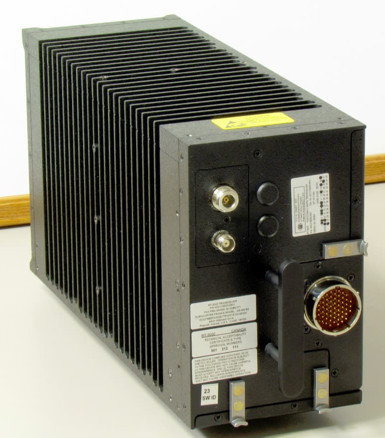
FRWRT-5000P-05
Dec 28, 201229.7 to 960 MHz Tactical Airborne Transceiver
Equipment Class
TNB - Licensed Non-Broadcast Station Transmitter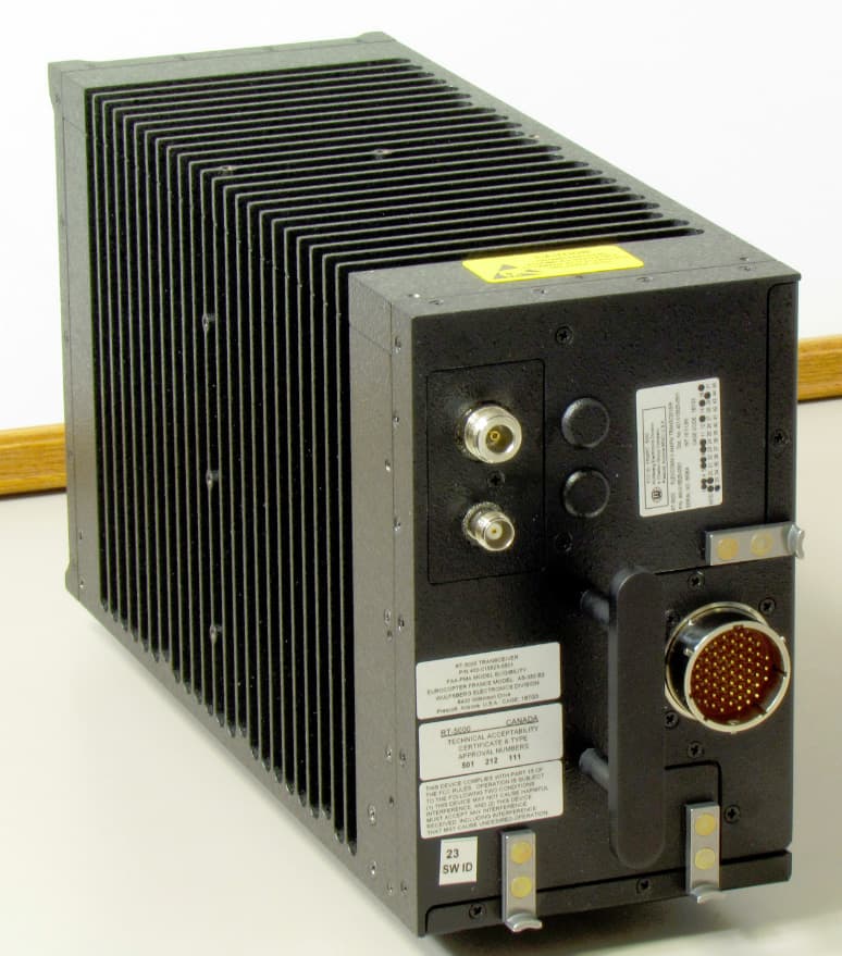
FRWRT-5000P-08
Dec 27, 201229.7 to 960 MHz Tactical Airborne Transceiver
Equipment Class
TNB - Licensed Non-Broadcast Station Transmitter