G6P1136Wireless Dosimetry
Sun Nuclear Corporation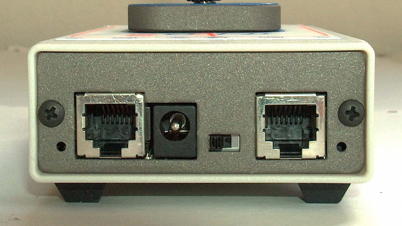
Click to zoom
Application Details
- Equipment Class
- DXT - Part 15 Low Power Transceiver, Rx Verified
- Date of Grant
- Sep 08, 2005
- Application Purpose
- Original Equipment
- Date of Application
- Jul 25, 2005
- Equipment Note
- Wireless Dosimetry
- Frequency Range
- 916.30000000 - 916.70000000
- Company
- Sun Nuclear Corporation
- Country
- United States
Documents & Files
Document Text
Text extracted from the exhibit documents filed with the FCC. Open a document above to read the original.
Users Manual
IVD Solutions™ User’s Guide Title Model 1136 rf-IVD 2 Model 1137 IVD 2 ii User’s Guide, IVD Solutions™ © Copyright 2002-2005 by Sun Nuclear Corporation. All rights reserved. The information contained in this technical manual and the accompanying software program are protected by copyright, and all rights are reserved by Sun Nuclear Corporation. Copying, duplicat- ing, selling, or otherwise distributing any part of this product without the prior written consent of Sun Nuclear Corporation is prohibited. Sun Nuclear Corporation reserves the right to make periodic modifications of this product without obligation to notify any person or entity of such revision. This guide is written for: Control Module firmware: version 2.00.00 Base/Pod firmware: version 2.00.00 PC software: version 2.00.00 IVD™, IVD 2 ™, rf-IVD™, rf-IVD 2 ™ and IVD Solutions™ are trademarks of Sun Nuclear Corporation. Other trademarks or trade names are the property of their respective owners. NOTICE: Model 1136 rf-IVD 2 ™ complies with Part 15 of the FCC Rules. Operation is subject to the following two conditions: (1) this device may not cause harmful interference, and (2) this device must accept any interference received, including interference that may cause undesired opera- tion. FCC ID: G6P1136 CAUTION: Recommended separation distance between rf-IVD 2 ™ and portable and mobile RF communications equipment (such as Bluetooth, cell phones, etc.) is 0.5 meter (20 inches). CAUTION: Any changes or modifications not expressly approved by Sun Nuclear Corporation could void the user's authority to operate this equipment. Document 1136011, Rev A, 5 July 2005 (not released) Sun Nuclear Corporation 425-A Pineda Court Melbourne, Florida 32940-7508 telephone 321-259-6862, fax 321-259-7979 e-mail: [email protected] http://www.sunnuclear.com iii Section 1. Introduction . . . . . . . . . . . . . 1 About IVD Solutions . . . . . . . . . . . . . . . . . . . . . . . . 1 Control devices . . . . . . . . . . . . . . . . . . . . . . . . . . . . 1 Control module . . . . . . . . . . . . . . . . . . . . . . . . . . 2 PC software . . . . . . . . . . . . . . . . . . . . . . . . . . . . 2 Applications. . . . . . . . . . . . . . . . . . . . . . . . . . . . . . . 3 Features . . . . . . . . . . . . . . . . . . . . . . . . . . . . . . . 3 Dose verification. . . . . . . . . . . . . . . . . . . . . . . . . 3 Total body irradiation (TBI) . . . . . . . . . . . . . . . . . 3 Diode selection and use . . . . . . . . . . . . . . . . . . . . . 4 Specifications . . . . . . . . . . . . . . . . . . . . . . . . . . . . . 5 How to use this guide . . . . . . . . . . . . . . . . . . . . . . . 7 Section 2. Installation . . . . . . . . . . . . . . 9 Unpacking . . . . . . . . . . . . . . . . . . . . . . . . . . . . . . . . 9 Connections . . . . . . . . . . . . . . . . . . . . . . . . . . . . . 10 Types of connections . . . . . . . . . . . . . . . . . . . . 10 Wireless connections . . . . . . . . . . . . . . . . . . . . 10 Wired connections . . . . . . . . . . . . . . . . . . . . . . 11 Connections with multiple pods . . . . . . . . . . . 12 Wall brackets. . . . . . . . . . . . . . . . . . . . . . . . . . . . . 13 Control module buttons and display . . . . . . . . . . . 14 Control module front panel . . . . . . . . . . . . . . . 14 Primary and alternate screens . . . . . . . . . . . . . 15 LEDs . . . . . . . . . . . . . . . . . . . . . . . . . . . . . . . . . 15 Function buttons . . . . . . . . . . . . . . . . . . . . . . . 15 Energy buttons/keypad. . . . . . . . . . . . . . . . . . . 16 Software installation . . . . . . . . . . . . . . . . . . . . . . . 16 Section 3. Control module operation . 17 Planning to use IVD Solutions . . . . . . . . . . . . . . . . 17 Energy keys . . . . . . . . . . . . . . . . . . . . . . . . . . . 17 Examples of system setup . . . . . . . . . . . . . . . . 17 Setup with control module . . . . . . . . . . . . . . . . . . 18 Initializing . . . . . . . . . . . . . . . . . . . . . . . . . . . . . 18 “Main” screen . . . . . . . . . . . . . . . . . . . . . . . . . . 19 Menu functions . . . . . . . . . . . . . . . . . . . . . . . . 19 Menu operation . . . . . . . . . . . . . . . . . . . . . . . . 19 Initial settings . . . . . . . . . . . . . . . . . . . . . . . . . . 20 Battery check . . . . . . . . . . . . . . . . . . . . . . . . . . 20 System select . . . . . . . . . . . . . . . . . . . . . . . . . . 20 Display adjust . . . . . . . . . . . . . . . . . . . . . . . . . . 21 Time and date. . . . . . . . . . . . . . . . . . . . . . . . . . 21 Software version. . . . . . . . . . . . . . . . . . . . . . . . 21 Dose calibration . . . . . . . . . . . . . . . . . . . . . . . . 22 View calibration . . . . . . . . . . . . . . . . . . . . . . . . 22 Temperature coef . . . . . . . . . . . . . . . . . . . . . . . 22 Dose unit setup . . . . . . . . . . . . . . . . . . . . . . . . 22 Device ID setup . . . . . . . . . . . . . . . . . . . . . . . . 22 PIN setup . . . . . . . . . . . . . . . . . . . . . . . . . . . . . 23 Physics mode . . . . . . . . . . . . . . . . . . . . . . . . . . 23 Institution name . . . . . . . . . . . . . . . . . . . . . . . . 24 Calibration with control module . . . . . . . . . . . . . . 24 Calibration overview . . . . . . . . . . . . . . . . . . . . . 24 Dose calibration . . . . . . . . . . . . . . . . . . . . . . . . 24 View calibration . . . . . . . . . . . . . . . . . . . . . . . . 26 Temperature coefficient (Tc) . . . . . . . . . . . . . . . . . 27 Temperature coefficient table . . . . . . . . . . . . 27 To enter Tc and V’ from table . . . . . . . . . . . . . 27 Temperature coefficient measurement . . . . . 28 Measurements with control module . . . . . . . . . . 32 Daily preparation (Model 1136). . . . . . . . . . . . 32 Measurement . . . . . . . . . . . . . . . . . . . . . . . . . 32 Data interpretation . . . . . . . . . . . . . . . . . . . . . 33 Solving operator problems . . . . . . . . . . . . . . . 34 Post operational checks (Mode…
Text truncated - open the document above for the full version.
Block Diagram
5 the start of the next RFA1 ON sequence should be set to sample the narrowest RF data pulse at least 10 times. Otherwise, significant edge jitter will be added to the detected data pulse. ASH Transceiver Block Diagram Figure 2 is the general block diagram of the ASH transceiver. Please refer to Figure 2 for the following discussions. Antenna Port The only external RF components needed for the transceiver are the antenna and its matching components. Antennas presenting an impedance in the range of 35 to 72 ohms resistive can be satisfacto - rily matched to the RFIO pin with a series matching coil and a shunt matching/ESD protection coil. Other antenna impedances can be matched using two or three components. For some impedances, two inductors and capacitor will be required. A DC path from RFIO to ground is required for ESD protection. Receiver Chain The output of the SAW filter drives amplifier RFA1. This amplifier in - cludes provisions for detecting the onset of saturation (AGC Set), and for switching between 35 dB of gain and 5 dB of gain (Gain Se - lect). AGC Set is an input to the AGC Control function, and Gain Se - lect is the AGC Control function output. ON/OFF control to RFA1 (and RFA2) is generated by the Pulse Generator & RF Amp Bias function. The output of RFA1 drives the SAW delay line, which has a nominal delay of 0.5 μs. The second amplifier, RFA2, provides 51 dB of gain below satura - tion. The output of RFA2 drives a full-wave detector with 19 dB of threshold gain. The onset of saturation in each section of RFA2 is detected and summed to provide a logarithmic response. This is added to the output of the full-wave detector to produce an overall detector response that is square law for low signal levels, and tran - sitions into a log response for high signal levels. This combination provides excellent threshold sensitivity and more than 70 dB of detector dynamic range. In combination with the 30 dB of AGC range in RFA1, more than 100 dB of receiver dynamic range is achieved. The detector output drives a gyrator filter. The filter provides a three-pole, 0.05 degree equiripple low-pass response with excellent group delay flatness and minimal pulse ringing. The 3 dB bandwidth of the filter can be set from 4.5 kHz to 1.8 MHz with an external re- sistor. The filter is followed by a base-band amplifier which boosts the de- tected signal to the BBOUT pin. When the receiver RF amplifiers are operating at a 50%-50% duty cycle, the BBOUT signal changes about 10 mV/dB, with a peak-to-peak signal level of up to 685 mV. For lower duty cycles, the mV/dB slope and peak-to-peak signal level are proportionately less. The detected signal is riding on a 1.1 Vdc level that varies somewhat with supply voltage, tempera - ture, etc. BBOUT is coupled to the CMPIN pin or to an external data recovery process (DSP, etc.) by a series capacitor. The correct value of the series capacitor depends on data rate, data run length, and other factors as discussed in theASH Transceiver Designer’s Guide. When an external data recovery process is used with AGC, BBOUT must be coupled to the external data recovery process and CMPIN by separate series coupling capacitors. The AGC reset function is driven by the signal applied to CMPIN. When the transceiver is placed in power-down (sleep) or in a trans - mit mode, the output impedance of BBOUT becomes very high. This feature helps preserve the charge on the coupling capacitor to mini - mize data slicer stabilization time when the transceiver switches back to the receive mode. Data Slicers The CMPIN pin drives two data slicers, which convert the analog signal from BBOUT back into a digital stream. The best data slicer choice depends on the system operating parameters. Data slicer DS1 is a capacitively-coupled comparator with provisions for an ad - justable threshold. DS1 provides the best performance at low Transceiver Block Diagram RFA1RFA2 TXA1TXA2 SAW Delay Line SAW CR Filter Log Antenna RFIO Tuning/ESD Detector Low-Pass Filter BB AGC Control Peak Detector Pulse Generator & RF Amp Bias LPFADJ PRATE PWIDTH RXDATA TXMOD CN TRL1 CN TRL0 AGCCAP R REF THLD2THLD1 Modulation & Bias Control Power Down Control Gain Select AGC Set AGC Reset Threshold Control BBOUT DS2 DS1 AND dB Below Peak Thld RefThld PKDET Ref AGC C BBO C PKD R LPF C AGC R PR R PW R TH2 R TH1 R TXM 20 8 17 18 14 15 3 9 56 4 7 13 1112 VCC1: Pin 2 VCC2: Pin 16 GND1: Pin 1 GND2: Pin 10 GND3: Pin 19 RREF: Pin 11 CMPIN: Pin 6 TX IN Tuning Figure 2 1 ® TR1000 916.50 MHz Hybrid Transceiver The TR1000 hybrid transceiver is ideal for short-range wireless data applications where robust operation, small size, low power consumption and low cost are required. The TR1000 employs RFM’s amplifier-sequenced hybrid (ASH) architecture to achieve this unique blend of character- istics. All critical RF functions are contained in the hybrid, simplifying and speeding design-in. The receiver section of the TR1000 is sensitive and stable. A wide dynamic range log detector, in combination with digital AGC and a compound data slicer, provide robust performance in the presence of on-channel interference or noise. Two stages of SAW filtering provide excellent re - ceiver out-of-band rejection. The transmitter includes provisions for both on-off keyed (OOK) and amplitude-shift keyed (ASK) modulation. The transmitter employs SAW filtering to suppress output harmonics, facilitating compliance with FCC 15.249 and similar regulations. RatingValueUnits Power Supply and All Input/Output Pins-0.3 to +4.0V Non-Operating Case Temperature-50 to +100 o C Soldering Temperature (10 seconds)230 o C CharacteristicSymNotesMinimumTypicalMaximumUnits Operating Frequencyf O 916.30916.70MHz Modulation TypeOOK Data Rate2.4kbps Receiver Performance (OOK @ 2.4 kbps) Input Current, 3 Vdc SupplyI R 1.8mA Input Signal for 10 -4 BER, 25°C 1-98dBm Rejection, ±30 MHzR REJ 55dB Transmitter Performance (OOK @ 2.4 kbps) Peak Input Current, 3 Vdc SupplyI TP 12mA Peak O…
Text truncated - open the document above for the full version.
Block Diagram
5 the start of the next RFA1 ON sequence should be set to sample the narrowest RF data pulse at least 10 times. Otherwise, significant edge jitter will be added to the detected data pulse. ASH Transceiver Block Diagram Figure 2 is the general block diagram of the ASH transceiver. Please refer to Figure 2 for the following discussions. Antenna Port The only external RF components needed for the transceiver are the antenna and its matching components. Antennas presenting an impedance in the range of 35 to 72 ohms resistive can be satisfacto - rily matched to the RFIO pin with a series matching coil and a shunt matching/ESD protection coil. Other antenna impedances can be matched using two or three components. For some impedances, two inductors and capacitor will be required. A DC path from RFIO to ground is required for ESD protection. Receiver Chain The output of the SAW filter drives amplifier RFA1. This amplifier in - cludes provisions for detecting the onset of saturation (AGC Set), and for switching between 35 dB of gain and 5 dB of gain (Gain Se - lect). AGC Set is an input to the AGC Control function, and Gain Se - lect is the AGC Control function output. ON/OFF control to RFA1 (and RFA2) is generated by the Pulse Generator & RF Amp Bias function. The output of RFA1 drives the SAW delay line, which has a nominal delay of 0.5 μs. The second amplifier, RFA2, provides 51 dB of gain below satura - tion. The output of RFA2 drives a full-wave detector with 19 dB of threshold gain. The onset of saturation in each section of RFA2 is detected and summed to provide a logarithmic response. This is added to the output of the full-wave detector to produce an overall detector response that is square law for low signal levels, and tran - sitions into a log response for high signal levels. This combination provides excellent threshold sensitivity and more than 70 dB of detector dynamic range. In combination with the 30 dB of AGC range in RFA1, more than 100 dB of receiver dynamic range is achieved. The detector output drives a gyrator filter. The filter provides a three-pole, 0.05 degree equiripple low-pass response with excellent group delay flatness and minimal pulse ringing. The 3 dB bandwidth of the filter can be set from 4.5 kHz to 1.8 MHz with an external re- sistor. The filter is followed by a base-band amplifier which boosts the de- tected signal to the BBOUT pin. When the receiver RF amplifiers are operating at a 50%-50% duty cycle, the BBOUT signal changes about 10 mV/dB, with a peak-to-peak signal level of up to 685 mV. For lower duty cycles, the mV/dB slope and peak-to-peak signal level are proportionately less. The detected signal is riding on a 1.1 Vdc level that varies somewhat with supply voltage, tempera - ture, etc. BBOUT is coupled to the CMPIN pin or to an external data recovery process (DSP, etc.) by a series capacitor. The correct value of the series capacitor depends on data rate, data run length, and other factors as discussed in theASH Transceiver Designer’s Guide. When an external data recovery process is used with AGC, BBOUT must be coupled to the external data recovery process and CMPIN by separate series coupling capacitors. The AGC reset function is driven by the signal applied to CMPIN. When the transceiver is placed in power-down (sleep) or in a trans - mit mode, the output impedance of BBOUT becomes very high. This feature helps preserve the charge on the coupling capacitor to mini - mize data slicer stabilization time when the transceiver switches back to the receive mode. Data Slicers The CMPIN pin drives two data slicers, which convert the analog signal from BBOUT back into a digital stream. The best data slicer choice depends on the system operating parameters. Data slicer DS1 is a capacitively-coupled comparator with provisions for an ad - justable threshold. DS1 provides the best performance at low Transceiver Block Diagram RFA1RFA2 TXA1TXA2 SAW Delay Line SAW CR Filter Log Antenna RFIO Tuning/ESD Detector Low-Pass Filter BB AGC Control Peak Detector Pulse Generator & RF Amp Bias LPFADJ PRATE PWIDTH RXDATA TXMOD CN TRL1 CN TRL0 AGCCAP R REF THLD2THLD1 Modulation & Bias Control Power Down Control Gain Select AGC Set AGC Reset Threshold Control BBOUT DS2 DS1 AND dB Below Peak Thld RefThld PKDET Ref AGC C BBO C PKD R LPF C AGC R PR R PW R TH2 R TH1 R TXM 20 8 17 18 14 15 3 9 56 4 7 13 1112 VCC1: Pin 2 VCC2: Pin 16 GND1: Pin 1 GND2: Pin 10 GND3: Pin 19 RREF: Pin 11 CMPIN: Pin 6 TX IN Tuning Figure 2 1 ® TR1000 916.50 MHz Hybrid Transceiver The TR1000 hybrid transceiver is ideal for short-range wireless data applications where robust operation, small size, low power consumption and low cost are required. The TR1000 employs RFM’s amplifier-sequenced hybrid (ASH) architecture to achieve this unique blend of character- istics. All critical RF functions are contained in the hybrid, simplifying and speeding design-in. The receiver section of the TR1000 is sensitive and stable. A wide dynamic range log detector, in combination with digital AGC and a compound data slicer, provide robust performance in the presence of on-channel interference or noise. Two stages of SAW filtering provide excellent re - ceiver out-of-band rejection. The transmitter includes provisions for both on-off keyed (OOK) and amplitude-shift keyed (ASK) modulation. The transmitter employs SAW filtering to suppress output harmonics, facilitating compliance with FCC 15.249 and similar regulations. RatingValueUnits Power Supply and All Input/Output Pins-0.3 to +4.0V Non-Operating Case Temperature-50 to +100 o C Soldering Temperature (10 seconds)230 o C CharacteristicSymNotesMinimumTypicalMaximumUnits Operating Frequencyf O 916.30916.70MHz Modulation TypeOOK Data Rate2.4kbps Receiver Performance (OOK @ 2.4 kbps) Input Current, 3 Vdc SupplyI R 1.8mA Input Signal for 10 -4 BER, 25°C 1-98dBm Rejection, ±30 MHzR REJ 55dB Transmitter Performance (OOK @ 2.4 kbps) Peak Input Current, 3 Vdc SupplyI TP 12mA Peak O…
Text truncated - open the document above for the full version.
External Photos
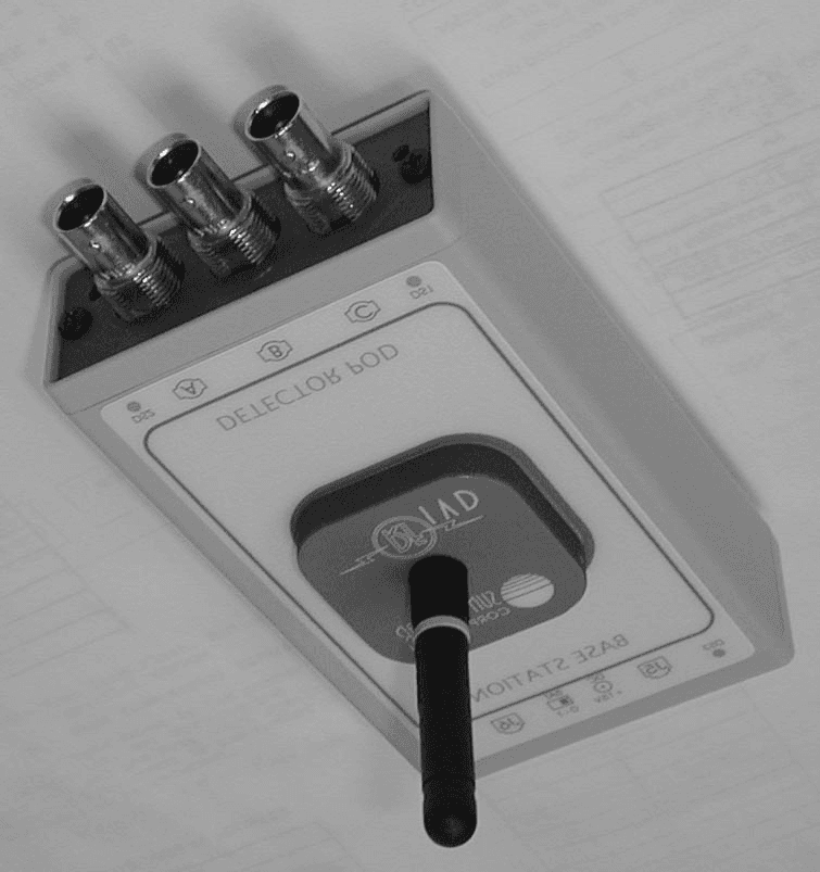
Bottom view. The label is metalized mylar of a type that we have been using for approximately 15 years for serial numbers on our products. They have proven very durable and it is located between the rubber feet where it will not be abraded.
External Photos
Bottom view. The label is metalized mylar of a type that we have been using for approximately 15 years for serial numbers on our products. They have proven very durable and it is located between the rubber feet where it will not be abraded.
ID Label/Location Info
- - 1 FCC ID LABEL/LOCATION Page 2 of this document is the second page of 1136 RF-IVD instruction manual with the appropriate labeling. The figure below is a picture of the unit with the FCC ID label attached. The label is a metallized mylar label that has an adhesive that gets progressively stronger over time. It is positioned on the bottom of the unit between the rubber feet so that it is not subject to abrasive damage in normal use. This label is of a type that we have been using for years to put serial numbers on our products. They have proven very durable. ii User’s Guide, IVD Solutions™ © Copyright 2002-2005 by Sun Nuclear Corporation. All rights reserved. The information contained in this technical manual and the accompanying software program are protected by copyright, and all rights are reserved by Sun Nuclear Corporation. Copying, duplicat- ing, selling, or otherwise distributing any part of this product without the prior written consent of Sun Nuclear Corporation is prohibited. Sun Nuclear Corporation reserves the right to make periodic modifications of this product without obligation to notify any person or entity of such revision. This guide is written for: Control Module firmware: version 2.00.00 Base/Pod firmware: version 2.00.00 PC software: version 2.00.00 IVD™, IVD 2 ™, rf-IVD™, rf-IVD 2 ™ and IVD Solutions™ are trademarks of Sun Nuclear Corporation. Other trademarks or trade names are the property of their respective owners. NOTICE: Model 1136 rf-IVD 2 ™ complies with Part 15 of the FCC Rules. Operation is subject to the following two conditions: (1) this device may not cause harmful interference, and (2) this device must accept any interference received, including interference that may cause undesired opera- tion. FCC ID: G6P1136 CAUTION: Recommended separation distance between rf-IVD 2 ™ and portable and mobile RF communications equipment (such as Bluetooth, cell phones, etc.) is 0.5 meter (20 inches). CAUTION: Any changes or modifications not expressly approved by Sun Nuclear Corporation could void the user's authority to operate this equipment. Document 1136011, Rev A, 5 July 2005 (not released) Sun Nuclear Corporation 425-A Pineda Court Melbourne, Florida 32940-7508 telephone 321-259-6862, fax 321-259-7979 e-mail: [email protected] http://www.sunnuclear.com
Internal Photos
RF-IVD, MODEL 1136, INTERNAL PHOTOGRAPHS The assemblies shown in Figure 1-3 consist of four Printed Circuit Board (PCB) assemblies. The lower board is the electrometer board. When it is used as a Diode Pod, it converts the current from the radiation detection diodes to digital values for transmission back to the Base Station. When it is used as a Base Station, it receives data from a Diode Pod and relays it to an Operator Module or a Personal Computer via a cable. The upper two boards shown in Figure 1 are the battery module and the RF transceiver. The fourth board is the antenna mounting pad (Not visible) located directly beneath the antenna. The first three boards slide into grooves in the extruded aluminum case. Figure 1 shows them as they are being removed from the case after the end panel has been removed. Figure 2 shows the assembly after the Battery module has been removed. Figure 3 shows the electrometer board after the RF transceiver has been unplugged. The blue cable connects the transceiver to the antenna. FIGURE 1 (Top View) Base Station/Diode Pod Assembly FIGURE 2 (Top View) Base Station/Diode Pod Assembly FIGURE 3 (Top View) Base Station/Diode Pod Assembly FIGURE 4A Top of Electrometer Assembly FIGURE 4B Bottom of Electrometer Assembly FIGURE 5A Top of RF Transceiver Assembly FIGURE 5B Bottom of RF Transceiver Assembly FIGURE 6A Antenna Mounting Pad, Top FIGURE 6B Antenna Mounting Pad, Bottom FIGURE 7A Battery Module, Top FIGURE 7B Battery Module, Bottom
Operational Description
OPERATIONAL DESCRIPTION Radio Frequency – In-Vivo Dosimeter "RF-IVD2" Model 1136 DESIGNED AND MANUFACTURED BY SUN NUCLEAR CORPORATION MELBOURNE, FL USA 321-259-6862 http://www.sunnuclear.com 1.0 Product Operational Overview The Sun Nuclear Model 1136 RF-IVD2 is a system that measures the radiation output of a radioactive substance such as a Co-60 source or a linear accelerator, during the treatment of a patient. Because the radioactive source is located near the middle of the treatment room an RF link makes the movement of personnel, patients and equipment around it safer, i.e. no cables to trip over and no cables to roll carts over. The system consists of 3 components: Display Module (user interface), Base Station (rf transmitter and receiver), and Detector Pod (rf transmitter and receiver). The Base Station and Detector Pod are identical and are interchangeable through system setup. The diode radiation detectors are connected to the Detector Pod through Lemo coaxial connectors. The radiation therapist connects the radiation detectors (diodes) to the Detector Pod and then positions them on the patient in order to measure the radiation from the accelerator. At this time, the patient is on the treatment couch of the accelerator, already positioned for treatment. The detector pod is battery operated and is positioned within 3 to 10 feet of the beam entrance to the patient. Also at this time, the beam is not on and the RF-IVD2 is not making a dose measurement. The therapist then leaves the treatment room that is shielded with approximately 3 feet of concrete and a heavy interlocked door. The patient is restrained on the couch because the treatment plan requires position accuracy to within millimeters, therefore no movement is allowed. Dose measurement is then remotely started on the RF-IVD2 from the Display Module in the control room and the accelerator beam turned on. A treatment fraction generally lasts for ½ minute or so. When the beam turns off, the RF-IVD2 is stopped and the dose value is displayed. The RF-IVD2 display value is recorded or printed on an accessory printer. The therapist then enters the room and removes the detector from the patient. The recorded RF-IVD2 measurement is a QA test that verifies the dose output during treatment from the radiation machine. The actual treatment plan is calculated in the Treatment Planning Computer (TPC – not part of the RF-IVD2) which uses dosimetry data acquired from a NIST traceable calibrated ion chamber and 3D water phantom. The plan output should also include the "expected" dose at the point of the IVD detector placement. Then the measured IVD dose and the expected TPC dose can be compared for verification. If the expected dose is not verified, the measured dose should not be used to adjust future treatments. Instead, an investigation should be conducted as to why the error occurred. The IVD is calibrated at the institution using the NIST traceable calibrated ion chamber as a standard, the same standard that is used to calibrate the accelerator and the TPC. Therefore, the IVD offers a closed loop QA test of the implementation of the plan. 2.0 RF Transceiver The RF Transceiver is a completely self-contained hybrid in a 7mm X 10mm, surface-mount, 20-terminal metal can. It operates at 916.5 MHz, +/- 0.2 MHz. The modulation is On/Off Keyed. We are using a baud rate of 4630 bits/sec. The data stream is Manchestered encoded. The manufacturer’s specification for the hybrid that we are using is attached to the back of this document. This hybrid is mounted on a two-sided circuit board with a bottom ground plane and a top copper poured ground plane around all of the circuit traces and component mounting pads. There is an 8-pin connector that connects the transceiver to the microcontroller based electrometer board beneath the transceiver’s printed circuit board . The transceiver gets its power, control and data thru the connector from the electrometer board. The transceiver’s power supply Voltage is 3.0V. The power is filtered to keep noise from the electrometer board from getting on the RF output. The two control lines place the transceiver in either transmit mode, receive mode or “Off” mode. There is one transmit line for data to the transceiver and one receive line for data from the transceiver. The RF output track on the printed circuit board from the transceiver hybrid is impedance matched to a 50 Ohm coaxial cable connector. The other end of the coaxial cable is plugged into another 50 Ohm connector that is soldered to the antenna mounting pad. The antenna mounting pad has a “Reverse SMA” connector that is not readily available to the consumer. The ¼ wave helical whip antenna mounts to the “Reverse SMA” connector. The case is an aluminum extrusion with metal end panels. The system has been tested to meet section 15.249 of Part 15. We are not measuring a patient biometric, i.e. a physical parameter of a human being. There is no electrical connection to the patient. We are measuring radiation coming from a radioactive isotope or a particle accelerator. A patient does not have to be present for this equipment to be used. 3.0 Location of Intended Use The radio frequency communication is only performed in the treatment vault of a hospital, clinic or university. The treatment vault is a shielded room having solid high density steel reinforced concrete walls and ceiling, a minimum of 3 feet thick. The door is an 8 inch thick steel and boron polycarbonate laminate. The treatment vault must be well shielded to protect personnel from very high energy x-rays (20 MV) and is built on the ground floor of the institution. The shielding to prevent high-energy x-rays from leaving the room also prevents RF energy from entering or leaving the room. Refer to the following System Block Diagram. 1 ® TR1000 916.50 MHz Hybrid Transceiver The TR1000 hybrid transceiver is ideal for short-range wireless data applications where robust operation, small size, low power co…
Text truncated - open the document above for the full version.
Test Report
RUBICOM SYSTEMS, INC. JUNE 2005 Rubicom Systems, Inc. 284 West Drive, Suite B Melbourne, Florida 32904 RSI EN 55011/FCC TEST REPORT FOR THE SUN NUCLEAR CORPORATION MODEL 1136/1137 WIRELESS rf-IVD² JA-2115-1 Sun Nuclear Corp. 1 EN 55011/FCC REPORT INTENTIONAL TRANSMITTER (CFR 47, PART 15.249) FOR THE SUN NUCLEAR CORPORATION rf-IVD² WIRELESS DOSIMETRY SYSTEM Prepared by: ________________________________________________ Joseph G. Barbee Tested by: ________________________________________________ Jason Gerke Performed by: Performed for: RUBICOM SYSTEMS, INC. SUN NUCLEAR CORPORATION 284 West Drive, Suite B 425-A Pineda Court Melbourne, Florida 32904 Melbourne, Florida 32940 FCC Registration Number: 90911 Completed: June 6, 2005 JA-2115-1 Sun Nuclear Corp. 2 TABLE OF CONTENTS Paragraph Title Page ABSTRACT............................................................................................................ 3 1.0 INTRODUCTION................................................................................................... 4 1.1 Purpose ................................................................................................................. 4 1.2 Requirements ........................................................................................................ 4 1.3 Unit Under Test Description .................................................................................. 4 1.4 Summary of Results .............................................................................................. 4 2.0 APPLICABLE DOCUMENTS............................................................................... 6 3.0 TEST SITE DESCRIPTION..............................................…
Text truncated - open the document above for the full version.
Contact Information
Applicant
William E. Simon(President)
Technical Contact
Sun Nuclear Corp.Randall E Karl
[email protected]321-259-6862
425 Pineda Court · Melbourne, Florida · United States
Test Firm
Advanced Compliance Solutions, Inc.Sam Wismer
Technical Specifications
| # | Rule Parts | Frequency Range | Power Output |
|---|---|---|---|
| 1 | 15C | 916.3 MHz - 916.7 MHz | - |
Other Applications from Sun Nuclear Corporation
G6P1133
Jan 17, 2001Wireless Dosimetry
Equipment Class
DXT - Part 15 Low Power Transceiver, Rx Verified