GAO-LT5000MISTTablet PC
Collage Investments LLC.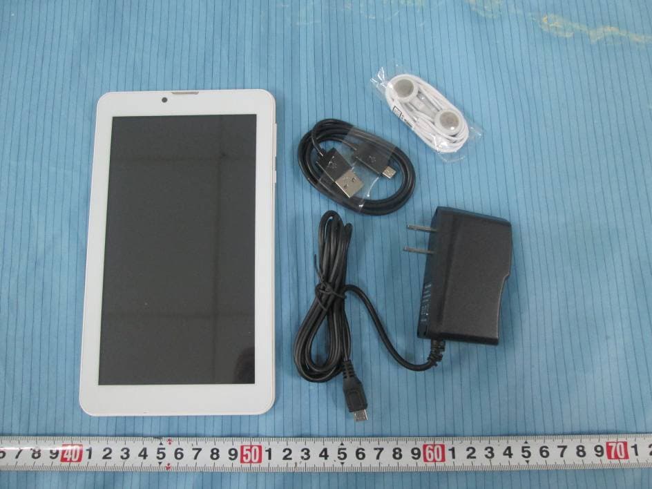
Click to zoom
Application Details
- Equipment Class
- PCE - PCS Licensed Transmitter held to ear
- Date of Grant
- Dec 04, 2014
- Application Purpose
- Original Equipment
- Date of Application
- Dec 04, 2014
- Equipment Note
- Tablet PC
- Frequency Range
- 1852.40000000 - 1907.60000000
- Company
- Collage Investments LLC.
- Country
- United States
Documents & Files
Document Text
Text extracted from the exhibit documents filed with the FCC. Open a document above to read the original.
Users Manual
1 2 Overview 1Introduction 1.1 Acknowledgement Thanks for your purchase of our product. This is highdefinition tablet PC. Its CPU is MTK8312 Dual core, it is based on Android 4.4.2 operation system, and easy to expand the third application procedure. The product is designed with various functions, including WIFI, BT, GPS, FM, voice call and so on. It is easy to achieve wireless communication and internet, you have access to surf the internet anytime and anywhere; it is also built with high accuracy GPS module, so that it can be used for navigating through installing map software. There are many sensors which offer you brand-new operation and entertainment; besides, it has camera shooting, which leads electronic consumption to enter into a fresh palm internet entertainment time. The manual systemically introduces the functions, use techniques and announcements, please read this manual carefully before your operation. Note: pictures and content are only used in the tablet as a function of signal, may be related to the actual product is different, please in kind prevail. 3 1.2 Announcements Preventive maintainance Please always keep the MID dry. To avoid the device short trouble, corrosion fault and electric short, please prevent the device, battery and charger from water and moisture, and don’t operate the device or charger by wet hand. To avoid failure of device, battery and charger, please prevent the device, battery, charger from violent shock or shake. To avoid failure of device, battery and charger, please prevent the device, battery, charger of all over heating or too cold circumstance. Never shock, throw, prod the MID, or drop, extrude, bend the MID. Never disassemble the device and accessories arbitrarily, otherwise the device and accessories are not in our company warranty scope. 1.3 Safety Instruction Before the operation of the MID, please read this chapter and teach your kids about these information. For further details, please refer to the safety instructions andannouncement. Never use the MID when driving car, in order to ensure safe driving. In the medical area, please abide by related rules and regulations. Please shut down the MID when it is near to the medical area. To avoid the wireless signal to interrupt the plane- controlled signal, please shut down the MID or using airplane mode when you are boarding a flight, To avoid electronic equipment failure, please shut down the MID in the vicinage of high-accuracy electronic equipments. Please don’t disassemble the MID and accessories. Only authorized agent has access to service the MID. Please keep the MID far away from magnetic equipments, the radiation of MID may erase the data stored in the magnetic equipments. Never use the MID in the vicinage of high temperature, inflammable gas (gas station). 1.4 2 2.1 Batt If . 2.2 Rem the The n belo P th P le P to N th 4 Abbrev Abbrevia MID 1 MID O tery Chargin f this naviga 2 MID minder icons When some screen to op e n you can clo ow status icon Protect the MI he MID witho Please comply egal rights wh Please strictly o ensure the s Never use the he MID from viation/T ation/Termin MID WIFI T F Intro Operation ng ator is first Status a remind mess en the remin ose the remin ns: New e m ID and access out parents’ s y with related hile using the adhere to rel safety of the M MID in bathr liquid wash Terminol nology Mo Wir Tra oducti n and Pr used, please and Rem sage appears nder list. Cho nder window mail 4 sories from k supervision. d rules and reg e MID. lated instructi MID or PC. room or othe or wet. logy Full Nam bile Internet reless Fideli ansFlash on reparatio e use AV ad minder in your remi oose the men through click kids reach sco gulations, and ions in the ma r humid envi me t Device ty on daptor to ful inder window nu you need, king the colu ope, and avoid d respect othe anual when u ronment, and D Mobile Inter Base onIEE wireless LAN Alternative n miniature me lly charge it w, please click and confirm umn to slide u Airplane Mo d the kids to u ers’privacyan using USB ca d please prote Description rnet Termina EE 802.11bg N name Micro emory card t. k column and m the informa up. Please ref ode on use nd able ect al gn standard SD, super d slip ation. fer to Re m Rem to vi Ope Whe finge 3.1 Key minder board minder icons w iew the detail en the remind en the remind er, then the re 1 Keys F ys Function D Power bu Vo l u m e + Vo l u m e - HOME( Back butt Display USB con Return b Displa a Current d will work wh led informatio der board der column sh eminder boar 3 Q unction Description: utton +(up) (down) (home) ton(back) recently-used nnected button ay recently-us application electric vol hile receiving on. hows new rem rd is opened. Quick d applicatio 5 sed lume emails, WIF minder icon, k Star Short pre shutdown increase t decrease Click it in click it in n display r e FI is open, you please hold t rt Gui ess to sleep/w n. the volume the volume n any interfac n any interfac ecently brow USB debugg Downloadin Home button WIFI conne av u can open th the column an ide wake up, long ce will return ce will return sed history ging connecte ng n ected, interne vailable he reminder b nd slip down press to star t n to main inter to previous m ed et is board your tup and rface. menu 6 Screenshot Intercept the current picture 3.2 Startup and Shutdown button Startup Long press POWER key for three seconds, you can enter into startup picture. The system enters into screen lock status, please unlock it Notice: When the MID has crashed, long press POWER key for elevenseconds to reset. Shutdown 1. Long press POWER, it will pop-up shutdown window. 2. Shutdown window contains Power off,Airplane mode and Audio profiles three options. 3. Click Power off is the last step. 3.3 Open and Close of the Screen Screen will be closed on its own when no operation happens. 1. Screen will be closed on its own if no operation happens for some time to save battery power 2. When sc…
Text truncated - open the document above for the full version.
External Photos
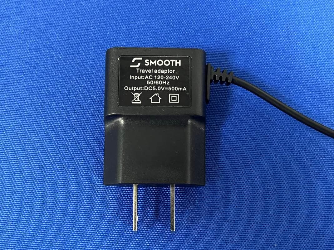
EXHIBIT B - EUT EXTERNAL PHOTOGRAPHS EUT – Full View EUT – Front View EUT – Rear View EUT – Top View EUT – Bottom View EUT – Left Side View EUT – Right Side View EUT – Adapter View
ID Label/Location Info
EXHIBIT A - FCC ID LABEL AND LOCATION FCC ID Label FCC ID Label Location Information The label shown shall be permanently affixed at a conspicuous location on the device and be readily visible to the user at the time purchase (Labeling requirements per 2.925)
Internal Photos
EXHIBIT C - EUT INTERNAL PHOTOGRAPHS EUT –Cover off View EUT – Main Board Top View BT/WIFI Antenna GSM/WCDMA Antenna EUT – Main Board Top Shielding Off View EUT – Main Board Bottom View EUT – LCD Top View EUT – LCD Bottom View
Operational Description
1 2G/3G Circuits Description Model: LT5000Mist Band: GSM850, GSM900, DCS1800, PCS1900, Wcma2100 1. Scope This document shows and provides the basic information about the platform we used.The more detail information about RF section are also included. M706r product is new Pad designed by HXMID .The base band circuit is base on MTK MT8312 and RF circuit is included Transceiver named MTK MT6166 , AP PA and skyworks PA, It works at five bands,GSM850,GSM900,DCS1800,PCS1900 wcma2100 2. Platform MT8312 is based on RF band support GSM+gps+wifi+Bluetooth+FM. The package supports dual-channel DDR2 using BGA package and EMMC flash device through SDIO interface. The GNSS+WIFI+Bluetooth +FM is MT6627 core. -Baseband functions,including mulitipe hareware cores -Single platform that provides dedicated support for all mardet leading codecs and other multimedia formats to support carrier deploymetnts around the word. -High-quality digital still image camera performance with up to 5-megarpixel resolution -HS-USB and OTG-USB core with built-in PHY eliminates additional USB components. -DC power reduction using innovative technique -integarates multiple processors -Supported two high speed DDR2 IC. 3. Tansceiver MT6166 The MT6166 is a RF transceiver targeted at high speed 2G multi-mod smart phone and tablet computers implanted in 40nm CMOS,The RF transceiver function is fully integrated. The document briefly introruces the RF mocros in MT6166 4. PA GSM AP6690 U616 is a transmit and receive Front End Module(FEM) designed is very low profile(0.9mm) and compact for factor for quad-band cellular handsets GSM850/GSM900/DCS1800/PC1900 operation –a complete transmit vco-to –Antenna and Antenna-to-receiver SAW filter solution.The FEM also supports Class 12 General Packet Radio Service(GPRS) multi-slot operation. Modes of operation: 2 Operating Parameters 5. WIFI/BT/FM/GPS operation block: MT6627 3 4
Parts List/Tune Up Info
1 HX-M706R-MB-V1.0.0-1MM-L6 PCS 1 2 NPO\0.5PF\0402\50V\±5%\R PCS 1 C715 3 NPO\1.5PF\0402\50V\±0.25PF\R PCS OR NPO\1.5PF\0402\50V\±0.25PF\R PCS 4 NPO\1.8PF\0402\50V\±0.1PF\R PCS 2 C671,C673 5 NPO\3.9PF\0402\50V\±0.25PF\R PCS 2 C668,C670 6 NPO\4.3PF\0402\50V\±1PF\R PCS 2 C662,C664 7 NPO\6.8PF\0402\50V\±0.25PF\R PCS 1 C730 8 NPO\18PF\0402\50V\±5%\R PCS 4 C319,C324,C489,C627 9 NPO\22PF\0402\50V\±5%\R PCS 7 C400,C439,C441,C442,C443,C467,C728 10 NPO\33PF\0402\50V\±5%\R PCS 15 C253,C254,C420,C422,C433,C445,C446,C447,C526 , C533 , C704 , C709 , C710 , C706 , C721 11 NPO\39PF\0402\50V\±5%\R PCS 1 C429 12 NPO\56PF\0402\50V\±5%\R PCS OR NPO\56PF\0402\50V\±5%\R PCS 13 NPO\100PF\0402\50V\±5%\R PCS 7 C222,C225,C255,C534,C705,C708,C10 14 14 NPO\220PF\0402\50V\±5%\R PCS 1 C435 15 X5R\152\0402\16V\±20%\R PCS 2 C665,C667 16 X7R\103\0402\50V\±10%\R PCS 6 C219,C527,C528,C529,C530,C531 17 X5R\104\0402\25V\±20%\R PCS 64 C104,C108,C109,C110,C111,C112,C113,C115,C116,C117,C120,C122,C123,C124,C125,C127,C128,C131,C138,C140,C142,C143,C144,C145,C148,C151,C156,C157,C158,C205,C206,C207,C221,C224,C241,C242,C243,C318,C320,C321,C403,C425,C438,C521,C522,C525,C535,C548,C623,C625,C711,C712,C832,C844,C1605,C1606,C431,C828,C831,C838,C729,C213,C621,C622 18 X5R\105\0402\25V±20%\R PCS OR X5R\105\0402\25V±20%\R PCS 19 X5R \ 105 \ 0603 \ 16V \ ±20% \ R PCS 5 C4 , C827 , C833 , C836 , C912 20 X5R\106\0603\10V\±20%\R PCS OR X5R\106\0603\10V\±20%\R PCS OR X5R\106\0603\25V\±20%\R PCS 21 X5R\106\0805\16V\±10%\R PCS OR X5R\106\0805\16V\±10%\R PCS 22 Y5V\224\0402\16V\±10%\R PCS 16 M706RV1.1.0 BOM 32 91 3 C470C490,C631,C716,C719,C723,C726C119,C152,C155,C216,C288,C304,C307,C308,C316,C322,C331,C352,C353,C404,C418,C448,C482,C547,C685,C820,C835,C846,C847,C857,C858,C909,C910,C1022,C1031,C1666,C632,C633C129,C132,C133,C134,C136,C153,C306,C311, C532C437C171 C220 C336 Page 1 M706RV1.1.0 BOM OR Y5V\224\0402\16V\±10%\R PCS 23 Y5V\225\0603\16V\±10%\R PCS OR Y5V\225\0603\25V\±10%\R PCS 24 X5R\226\0805\6.3V\±20%\R PCS OR X5R\226\0805\6.3V\±20%\R PCS 25 X7R\472\0402\50V\±10%\R PCS 1 C217 26 X5R\474\0402\6.3V\±10%\R PCS 6 C469,C474,C475,C476,C477,C484 27 X5R\475\0402\10V\±20%\R PCS OR X5R\475\0402\10V\±20%\R PCS 28 Y5V\475\0603\6.3V\±10%\R PCS OR Y5V\475\0603\10V\±10%\R PCS 29 Y5V\475\0805\25V\±10%\R PCS 1 C850 30 0.056R\0805\±1%\1/8W\R PCS 1 R328 31 0R\0402\±5%\1/16W\R PCS 52 R301,R322,R340,R402,L405,R414,R420,R421,R422,R423,R425,R437,R442,R443,R675,R836,R857,R916,C1011,R1021,R1022,R1023,R1024,R1208,R1623,R1624,R1659,R1661,R427,R1664,R1665,R44,R417,R428,L430,R856,R859,R332,R336,R430,R434,R435,R677,R617,R618,R1070,R1071 , R1009 , R1010 , R1006 , R432 , R1028 32 0R\0603\±5%\1/10W\R PCS 1 L804 33 2.2R\0603\±1%\1/10W\R PCS 1 R850 34 10R\0402\±5%\1/12W\R PCS 1 R1682 35 26.1R\0402\±1%\1/16W\R PCS 3 R521,R624,R628 36 34.8R\0402\±1%\1/16W\R PCS 1 R627 37 51R\0402\±5%\1/16W\R PCS 1 R620 38 100R\0402\±5%\1/16W\R PCS 2 R507,R508 39 240R\0402\±1%\1/16W\R PCS 1 R511 40 330R\0402\±5%\1/16W\R PCS 2 R837,R841 41 470R\0402\±5%\1/16W\R PCS 2 R407,R408 42 1K\0402\±5%\1/16W\R PCS 16 R95,R316,R403,R410,R415,R441,R516,R714,R717R835,R843 , R904 , R905 , R1011 , R910 , R912 43 1K\0402\±1%\1/16W\R PCS 1 R842 44 1.5K\0402\±5%\1/16W\R PCS 2 R203,R515 45 1.5K\0402\±1%\1/16W\R PCS 2 R715,R716 3 13 41 11 C171 , C220 , C336 C218,C334,C545,C546,C840,C542,C539,C540C841,C848,C1615,C906,C859C341,C519,C520,C449C834C130,C223,C301,C302,C303,C309,C333,C335,C406,C426,C713, Page 2 M706RV1.1.0 BOM 46 2K\0402\±1%\1/16W\R PCS 2 R400,R97 47 2.2K\0402\±1%\1/16W\R PCS 1 R848 48 3.3K\0402\±1%\1/16W\R PCS 1 R339 49 4.7K\0402\±5%\1/16W\R PCS 7 R217,R218,R220,R222,R223,R224,R853 50 5.11K\0402\±1%\1/16W\R PCS 1 R201 51 8.06K\0402\±1%\1/12W\R PCS 2 R209,R211 52 10K\0402\±5%\1/16W\R PCS 8 R24,R405,R406,R863,R412,R831,R833,R84 5 53 15K\0402\±1%\1/16W\R PCS 1 R828 54 12K\0402\±5%\1/16W\R PCS 1 R840 55 20K\0402\±1%\1/16W\R PCS 1 R907 56 24K\0402\±5%\1/16W\R PCS 1 R440 57 27K\0402\±1%\1/16W\R PCS 1 R906 58 39K\0402\±1%\1/16W\R PCS 1 R325 59 47K\0402\±5%\1/16W\R PCS 2 R456,R849 60 6.8K\0402\±1%\1/16W\R PCS 1 R838 61 330K\0402\±1%\1/16W\R PCS 1 R330 62 470K\0402\±5%\1/16W\R PCS 2 R404,R454 63 1nH\0402\±0.3nH\R PCS 3 C701,C707,C732 64 1.2nH\0402\±0.3nH\R PCS 1 C700 65 1.8nH\0402\±0.3NH%\R PCS 1 L601 66 2nH\0402\±0.3nH\R PCS 1 L630 67 2.2nH\0402\±0.3nH\R PCS 1 L418 68 2.7nH\0402\±0.3nH\R PCS 1 L619 69 3nH\0402\±0.3nH\R PCS 1 L422 70 4.3nH\0402\±0.3nH\R PCS 1 L617 71 5.6nH\0402\±0.3nH\R PCS 1 L602 72 6.2nH\0402\±0.3nH\R PCS 2 L423,L426 73 7.5nH\0402\±5%\R PCS 1 L425 74 9.1nH\0402\±5%\R PCS 1 L604 75 12nH\0402\±5%\R PCS 3 L400,L419,L603 76 22nH\0402\±5%\R PCS 1 C702 77 27nH\0402\±0.3nH\R PCS 1 C606 78 33nH\0402\±5%\R PCS 2 L618,L626 Page 3 M706RV1.1.0 BOM 79 39nH\0402\±5%\R PCS 1 L416 80 82nH\0402\±5%\R PCS 1 L1006 81 2.5K@100MHZ\50MA\0603 PCS 3 BEAD410,BEAD411,L402 82 1.8K ohm\50mA\0402 PCS OR 1.8K ohm\50mA\0402 PCS 83 0.68uH \ 3.3A0.42R \ ±20% \ 2.5*2.0*1.2mm \ R PCS OR 0.68uH \ 3.3A \ 0.42R \ ±20% \ 2.5*2.0*1.2mm \ R PCS OR 0.68uH \ 3.3A \ 0.065R \ ±30% \ 2.5*2.0*1.2mm \ R PCS 84 1uH \ 2.2A \ 0.073R \ ±30% \ 2.5*2.0*1.1mm PCS OR 1uH \ 2.2A \ 0.073R \ ±30% \ 2.5*2.0*1.1mm PCS OR 1uH \ 2.2A \ 0.073R \ ±30% \ 2.5*2.0*1.2mm PCS 85 22uH \ 0.57A \ ±20% \ 3.0*3.0*1.5mm \ R PCS OR 22uH \ 0.57A \ ±20% \ 3.0*3.0*1.5mm \ R PCS 86 BAT54S\200MA\SOT-23\R PCS OR BAT54S \ SOT-23 \ 200MA \ SOT-23 \ R PCS 87 RB160M-30\1A\SOD-123\R PCS 2 D802,D807 88 5.1V\1206 PCS 1 D302 89 NPN\MMBT3904\200mA\SOT-23\R PCS OR NPN\LMBT3904LT1\200mA\SOT-23\R PCS 90 AO3423\2A\SOT-23\R PCS OR AO3423\2A\SOT-23\R PCS 91 IC\CPU\MT8312V/X_WCDMA1.3GHZ\11*10.6*0.9MM\VFPGA475L PCS 1 U201 92 IC\LPDDR2-128*32*2\1GB \Clock_800MHZ\K4P8G304EB-AGC1 \1.2V\168-ball FBGA\R PCS 1 U1 93 IC\TD2514WFA\2.5-5.5V\12V\SOT-23-6L\R PCS OR IC\AP3128\2.5-5.5V\12V\SOT-23-6L\R PCS OR IC\TCS5514\2.5-5.5V\12V\SOT-23-6L\R PCS 94 IC\TCS3354\2.5-5.5V\28V\SOT-23-5L\R PCS 1 U804 95 IC\MT6627\MQFN40\5*5*0.4mm\R PCS 1 U2 96 IC\MT6166\TD-SCDMA\4.6*4.6\TFBGA104\R PCS 1 U400 97 IC\MT6323A\3.4-4…
Text truncated - open the document above for the full version.
Parts List/Tune Up Info
1 Tune-Up Procedure Tune-Up TX Content 1 Purpose............................................................................................................................. 2 2 General description ..........................................................................................................3 2.1 Characteristics of the transmit burst..................................................................... ......3 2.2 GPRS/Edge Data ransfer................................................................................................3 2.2.1 GSM850&PCS1900 allowed maximum output reduction in a multislot...............3 2.2.2 Edge power description........................................................................4 2.3 UMTS Band2 and Band5 allowed maximum output power Configuration..............4 3 Parameters........................................................................................................................ 4 3.1 Parameters used to shape the burst....................................................................... ......4 3.2 Parameters used to define the temporal position of the burst....................................... 4 3.2.1 Optimum position of the burst................................................................................... 4 3.2.2 Optimum length of the burst...................................................................................... 5 4 Operating mode ................................................................................................................5 4.1 How to transmit a Tch burst (Random data), in GSM850 PCS1900 mode, at power control level max: .............................................................................................................. 5 4.2 How to stop Tx measurements: .................................................................................... 5 4.3 How to transmit a burst after modifying parameters.................................................... 6 5 Purpose............................................................................................................................. 6 6 Automatic frequency control ...........................................................................................6 7 Static frequency error and range.......................................................................................8 2 1 Purpose This panel gives the possibility to manage the mobile in the transmit mode. This window includes both: - All the parameters (frequency band, RF channel, RF level to get the desire antenna output power...) The user needs to make the mobile transmitting, - All the parameters needed to define a transmit burst, - All the compensation table to be able to align the mobile in production. This Tx_commands user guide is describing: - The characteristics of the transmit burst, - All the parameters used in the transmit mode, - The operating mode to make the mobile transmitting 3 2 General description 2.1 Characteristics of the transmit burst for GSM850/PCS The power levels and the shape of a transmit burst are controlled by the power amplifier controller integrated in the MT83 12. The burst is generated by a 10-bit DAC from the MT8312 as shown below: The ramping shape is referenced with the rising edge of Tx-ON (from the Baseband). There are two types of parameters define the transmit burst: the first one define the shapes of the burst, and the second one define the temporal position of the burst. The rising and the falling edge of the transmit burst are determined by a set of 32 DAC code values n = 0 ... 31. Tru = TxTRUDefault + △TRU_P + △TRU_T Trd = TxTRD_NBDefault + △TRD_P (for a normal burst). Trd = TxTRD_ABDefault + △TRD_P (for an access burst). 2.2 GPRS Data Transfer for GSM850/PCS1900 2.2.1 GSM850&PCS1900 allowed maximum output reduction in a multislot GSM mobile phones use a Time Division Multiple Access (TDMA) scheme to transmit data. The TDMA format contains eight time slots. The handset power amplifier typically transmits in four of these up time slots. To prevent interference between cell phones, the time mask profile as specified is very restricted. To meet the GSM time mask, the output power of the PA needs to ramp up and down very quickly while staying within the time mask and not 4 generating extraneous frequency bursts due to too abrupt ramp profiles. As described before, the Vramp input value sets the RF output power. By applying a certain ramp profile to the Vramp pin, the power level (Pout) of the PA is set to obtain the required time mask. A time mask of the PA’s output power is displayed. The time mask meets the limits (displayed by green lines) over a wide range of temperature, voltage and load variations. 2.2.2 Edge power transmit description The direct modulation transmitter (8PSK),combined with a low noise GMSK constant envelope modulator or DFM(Direct-Frequency Modulation),delivers high modulation accuracy with exceptionally low noise and eliminates the need for tansmit SAW filters in any of the supported GGE bands. The max Edge power for GSM850 is tipically 26.5dBm with the range 26-27.6dBm for MTK; The max Edge power for PCS is tipically 25.5dBm with the range 24-27.0dBm for MTK; 2.3 UMTS Band2 and Band5 transmit max power Max power range for both band2 and band5 listed as below: Transmitter consists of 5 output ports.TX_LB2 and TX_HB1 ports are multi-mode ports which can support 2G or 3G depending on application circuits on the phone. Typ. maximum TX output power is>0dBm.Overall TX gain dynamic range is 78dB in RF and 8dB in BB. The power detections circuits are also included for better power accuracy over power region of PA gain mode change. In order to ensure power detection accuracy, the PCB trace to DET pin should not be put too close to TX output signal traces. 5 3 Parameters F (n) are values coming from the DAC to shape the transmit burst. Some F(n) values have a corresponding Parameter used in the TAT to align the mobile…
Text truncated - open the document above for the full version.
RF Exposure Info
Note: This test report is prepared for the customer shown above and for the equipment described herein. It may not be duplicated or used in part without prior written consent from Bay Area Compliance Laboratories Corp. SAR EVALUATION REPORT For Collage Investments LLC. 11437 NW 34 STREET, DORAL, FLORIDA 33178 U.S.A FCC ID: GAO-LT5000MIST Report Type: Original Report Product Type: Tablet PC Test Engineer: Wilson Chen Report Number: RSZ141022003-20 Report Date: 2014-11-15 Reviewed By: Bell Hu SAR Engineer Prepared By: Bay Area Compliance Laboratories Corp. (Shenzhen) 6/F, the 3rd Phase of WanLi Industrial Building, ShiHua Road, FuTian Free Trade Zone Shenzhen, Guangdong, China Tel: +86-755-33320018 Fax: +86-755-33320008 www.baclcorp.com.cn Bay Area Compliance Laboratories Corp. (Shenzhen) Report No: RSZ141022003-20 SAR Evaluation Report 2 of 94 Attestation of Test Results EUT Information Company Name Collage Investments LLC. EUT Description Tablet PC FCC ID GAO-LT5000MIST Model Number LT5000Mist Test Date 2014-11-02 Frequency Max. SAR Level(s) Reported Limit(W/Kg) GSM 850 0.352 W/kg 1g Head SAR 1. 6 0.755 W/kg 1g Body SAR PCS 1900 0.265 W/kg 1g Head SAR 1.143 W/kg 1g Body SAR WCDMA850 0.120 W/kg 1g Head SAR 0.371 W/kg 1g Body SAR WCDMA1900 0.320 W/kg 1g Head SAR 1.192 W/kg 1g Body SAR Simultaneous 0.742 W/kg 1g Head SAR 1.582 W/kg 1g Body SAR Applicable Standards ANSI / IEEE C95.1 : 2005 IEEE Standard for Safety Levels with Respect to Human Exposure to Radio Frequency Electromagnetic Fileds,3 kHz to 300 GHz. ANSI / IEEE C95.3 : 2002 IEEE Recommended Practice for Measurements and Computations of Radio Frequency Electromagnetic Fields With Respect to Human Exposure to SuchFields,100 kHz—300 GHz. IEEE1528:2013 IEEE Recommended Practice for Determining the Peak Spatial-Average Specific Absorption Rate (SAR) in the Human Head from Wireless Communications Devices: Measurement Techniques KDB procedures KDB 447498 D01 Mobile and Portable Devices RF Exposure Procedures and Equipment Authorization Policies. KDB 648474 D04 SAR Evaluation Considerations for Wireless Handsets KDB 865664 D01SAR Measurement Requirements for 100 MHz to 6 GHz KDB 616217 D04 SAR for laptop and tablets v01r01 KDB 941225 D01 SAR Measurement Procedures for 3G Devices-CDMA 2000/EV-Do WCDMA/HSDPA/HSUPA KDB 941225 D06 SAR Evaluation Procedures for Portable Devices with Wireless Router Capabilities. Note: This wireless device has been shown to be capable of compliance for localized specific absorption rate (SAR) for General Population/Uncontrolled Exposure limits specified in ANSI/IEEE Standards and has been tested in accordance with the measurement procedures specified in IEEE 1528-2013 and RF exposure KDB procedures. The results and statements contained in this report pertain only to the device(s) evaluated. Bay Area Compliance Laboratories Corp. (Shenzhen) Report No: RSZ141022003-20 SAR Evaluation Report 3 of 94 TABLE OF CONTENTS DOCUMENT REVISION HISTORY ......................................................................................................................... 5 EUT DESCRIPTION .................................................................................................................................................... 6 TECHNICAL SPECIFICATION ......................................................................................................................................... 6 REFERENCE, STANDARDS, AND GUILDELINES ............................................................................................... 7 SAR LIMITS ................................................................................................................................................................. 8 FACILITIES .................................................................................................................................................................. 9 DESCRIPTION OF TEST SYSTEM ........................................................................................................................ 10 EQUIPMENT LIST AND CALIBRATION ............................................................................................................. 17 EQUIPMENTS LIST & CALIBRATION INFORMATION .................................................................................................... 17 SAR MEASUREMENT SYSTEM VERIFICATION .............................................................................................. 18 LIQUID VERIFICATION ............................................................................................................................................... 18 SYSTEM ACCURACY VERIFICATION ........................................................................................................................... 21 SAR SYSTEM VALIDATION DATA ..................................................................................................................... 22 EUT TEST STRATEGY AND METHODOLOGY ................................................................................................. 30 TEST POSITIONS FOR DEVICE OPERATING NEXT TO A PERSON’S EAR........................................................................ 30 CHEEK/TOUCH POSITION ........................................................................................................................................... 31 EAR/TILT POSITION ................................................................................................................................................... 31 TEST POSITIONS FOR BODY-WORN AND OTHER CONFIGURATIONS .............................................................................. 32 SAR EVALUATION PROCEDURE ................................................................................................................................. 33 TEST METHODOLOGY ..................................................................................................................................…
Text truncated - open the document above for the full version.
Schematics
5 5 4 4 3 3 2 2 1 1 DD CC BB AA check MSDC1/2 IO power C115 close to pin E1 (150mil) C125 close to pin G26 (150mil) VCCK_VPROC VCCK To MT6323 VPROC_FB pin (1)VPROC_BB, GND pin of 1st cap group should be laid differential pair with ground shielding remote sense to PMIC To MT6323 GND_VPROC_FB pin (2)R107 & R103 must be close to 1st cap group. If you want to remove them, please make sure the VPROC_FB/GND_VPROC_FB must connect from 1st cap. group of VPROC 1.2V IO for DDR2 DDR3VCCIO VTCXO_PMU VIO18_PMU VIO18_PMU VIO18_PMU VUSB_PMU VIO18_PMU VIO18_PMU VMC_PMU VIO18_PMU VPROC_PMU VIO18_PMU VIO18_PMU VIO28_PMU VM_PMU DVDD12_EMI VPROC_FB3 GND_VPROC_FB3 Title SizeDocument NumberRev Date:Sheet of MT8312 TABLET V1.0 01 MT8312 - Power C 122Wednesday, December 03, 2014 Title SizeDocument NumberRev Date:Sheet of MT8312 TABLET V1.0 01 MT8312 - Power C 122Wednesday, December 03, 2014 Title SizeDocument NumberRev Date:Sheet of MT8312 TABLET V1.0 01 MT8312 - Power C 122Wednesday, December 03, 2014 C132 10uF/C0603 2 1 C151 100nF/C0402 2 1 C104 100nF/C0402 2 1 C148 100nF/C0402 2 1 C112 100nF/C0402 2 1 C117 100nF/C0402 2 1 C131 100nF/C0402 2 1 C110 100nF/C0402 2 1 C125 100nF/C0402 2 1 C113 100nF/C0402 2 1 C109 100nF/C0402 2 1 C145 100nF/C0402 2 1 C111 100nF/C0402 2 1 C129 10uF/C0603 2 1 C133 10uF/C0603 2 1 C143 100nF/C0402 2 1 C140 100nF/C0402 2 1 C116 100nF/C0402 2 1 C156 100nF/C0402 2 1 C108 100nF/C0402 2 1 MT8312 U201B DVSS A19 DVSS A26 DVSS B4 DVSS B10 DVDD12_EMI E7 DVDD12_EMI F7 DVDD12_EMI F8 DVDD12_EMI G8 AVSS18_MD U20 AVSS18_WBG U7 AVSS18_WBG V7 AVSS18_MD U21 DVSS B12 DVSS B14 DVSS B17 DVSS B22 DVSS B24 DVSS C4 DVSS C8 DVSS C11 DVSS C12 DVSS C16 DVSS C17 DVSS C18 DVSS C20 DVSS C21 DVSS C22 DVSS C23 DVSS C25 DVSS D4 DVSS D5 DVSS D7 DVSS D9 DVSS D11 DVSS D13 DVSS D15 DVSS D17 DVSS D21 DVSS D24 DVSS E5 DVSS E8 DVSS E10 DVSS E18 DVSS E21 DVSS F6 DVDD28_MSDC1 E1 DVDD28_MSDC2 V1 DVDD28_BPI AD26 DVDD28_MD U25 DVDD18_IO1 Y26 DVDD18_IO2 D1 DVDD18_IO3 W1 DVDD18_IO4 AG13 AVSS18_WBG W7 AVSS18_WBG Y7 AVSS18_WBG AB6 AVSS18_WBG AB8 AVSS18_WBG AC3 VCCK L11 VCCK L12 VCCK L13 VCCK L14 VCCK L15 VCCK L16 VCCK L17 VCCK M10 VCCK M18 VCCK N10 VCCK N18 AVDD18_MD AE21 AVSS18_MD V20 AVSS18_MD V21 AVDD18_AP AE19 AVDD28_DAC AE22 DVDD18_PLLGP AE18 AVDD18_MEMPLL A3 AVSS18_MEMPLL A2 DVDD18_MIPITX L2 DVDD18_MIPIIO G1 AVDD33_USB T24 AVDD18_USB P26 AVSS33_USB R24 DVDD12_EMI G9 DVDD12_EMI G11 DVDD12_EMI G13 DVDD12_EMI G15 DVDD12_EMI G16 DVDD12_EMI G18 DVDD12_EMI H8 DVSS F18 DVSS18_MIPIIO H4 DVSS18_MIPITX L4 DVDD12_EMI H11 DVDD12_EMI H13 DVSS G6 DVSS G7 DVSS G14 DVSS G17 DVSS G20 DVSS H10 DVSS L10 DVSS L18 DVSS M12 DVSS M13 DVSS M14 DVSS M15 DVSS M20 DVSS N11 DVSS N21 DVSS P10 DVSS P11 DVSS P12 DVSS P13 DVSS P16 DVSS P17 VCCK P9 VCCK P18 VCCK R9 DVDD18_IO0 L26 DVSS P21 VCCK R10 AVSS18_MD W20 DVDD12_EMI H15 DVDD12_EMI H16 DVDD12_EMI H18 DVDD18_MSDC0 G26 VCCK R18 DVSS R2 DVSS R11 DVSS T11 AVSS18_WBG AC5 AVSS18_WBG AC7 AVSS18_WBG AD4 AVSS18_WBG AE3 AVSS18_MD W21 AVSS18_MD Y20 AVSS18_MD Y21 AVSS18_MD AA21 AVSS18_MD AB21 AVSS18_AP U17 AVSS18_AP U18 AVSS18_WBG AE5 DVSS T13 DVSS T16 DVSS T17 DVSS T18 DVSS T21 DVSS M11 DVSS U11 DVSS U12 DVSS V11 DVSS V12 DVSS V13 DVSS M16 DVSS K21 DVSS M17 DVSS H12 DVSS J21 DVSS H20 DVSS H17 DVSS H14 VCCK_VPROC N12 VCCK_VPROC N13 VCCK_VPROC N14 VCCK_VPROC N15 VCCK_VPROC N16 VCCK_VPROC N17 VCCK_VPROC P14 VCCK_VPROC R15 VCCK_VPROC P15 VCCK_VPROC R14 VCCK_VPROC R13 VCCK_VPROC R12 VCCK_VPROC R16 V…
Text truncated - open the document above for the full version.
Contact Information
Applicant
Daniel Esteban Gonzalez(Manager)
Test Firm
Bay Area Compliance Laboratory Corp. (Shenzhen)John Chan
Technical Specifications
| # | Rule Parts | Frequency Range | Power Output | Emission | Tolerance |
|---|---|---|---|---|---|
| 4 | 24E | 1.85 GHz - 1.91 GHz | 157.00 mW | 4M19F9W | 2.5 ppm |
Other Applications from Collage Investments LLC.
GAO-FLIP4G
Nov 30, 2023Mobile Phone
Equipment Class
DTS - Digital Transmission System
GAO-VISPLU
Jan 30, 2023Smartphone
Equipment Class
DTS - Digital Transmission System
GAO-VISION
Jan 17, 2023Smartphone
Equipment Class
PCE - PCS Licensed Transmitter held to ear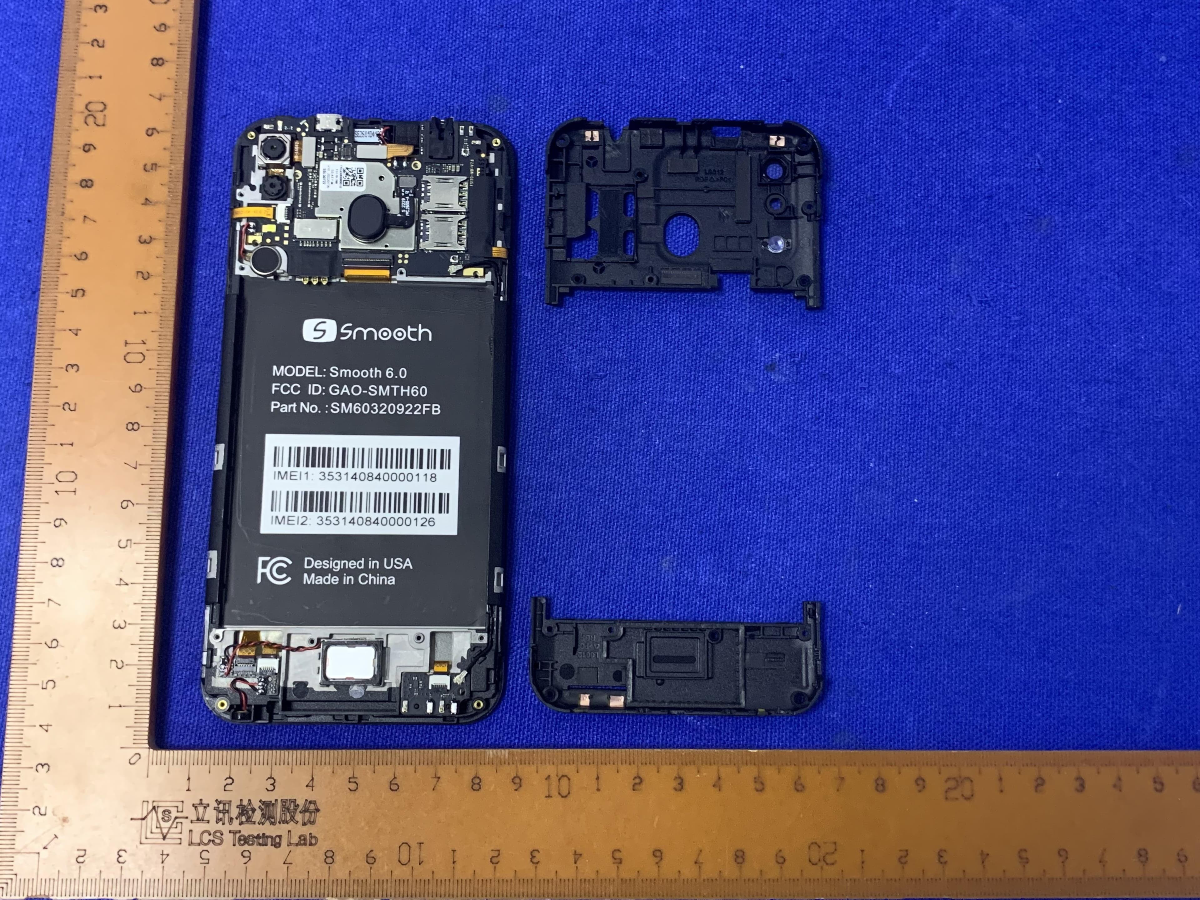
GAO-SMTH60
Oct 13, 2022Smart phone
Equipment Class
DSS - Part 15 Spread Spectrum Transmitter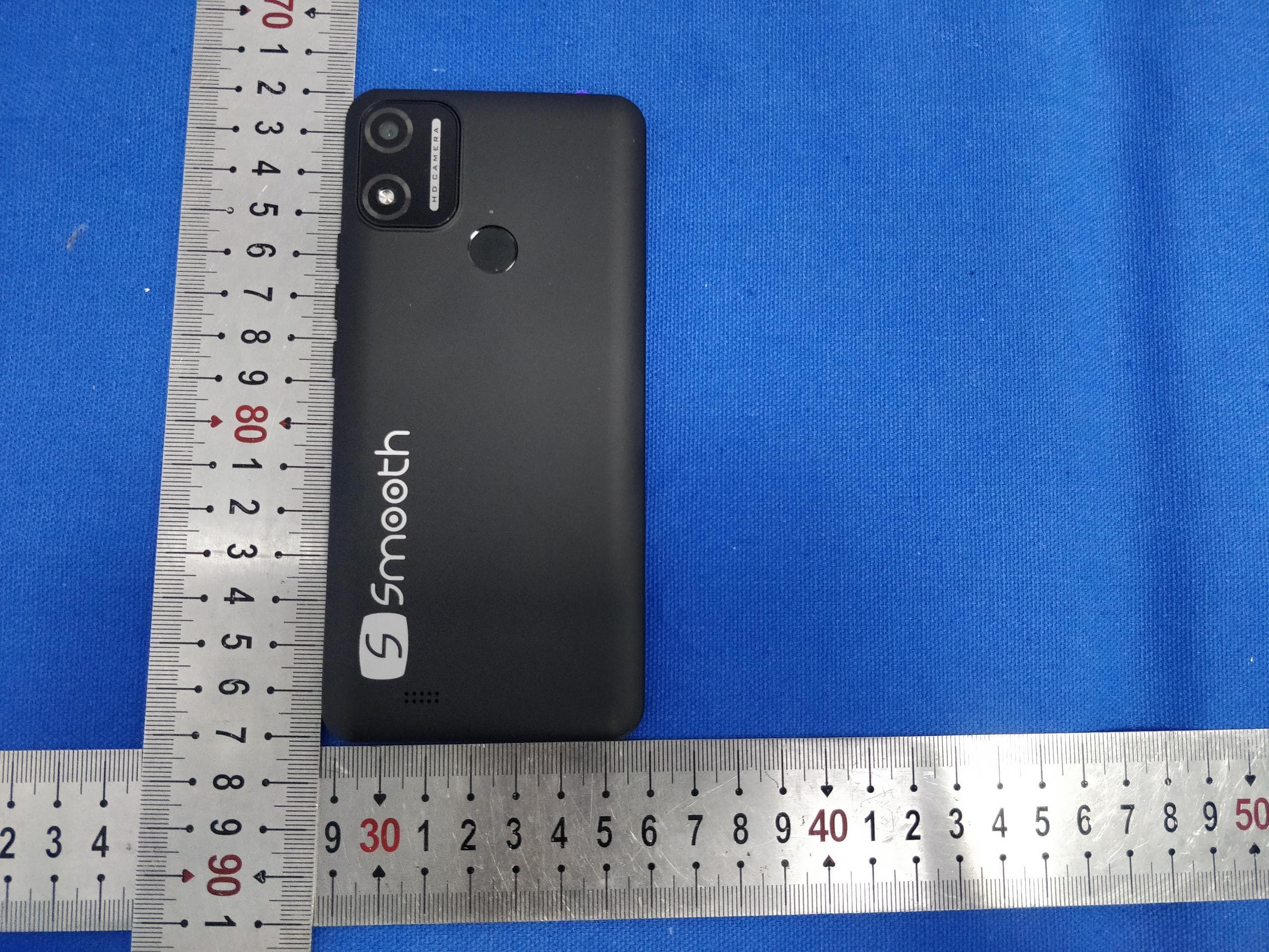
GAO-55MAX22
Jun 07, 2022Smart phone
Equipment Class
PCE - PCS Licensed Transmitter held to ear