GAO-MAX403G smartphone
Collage Investments LLC.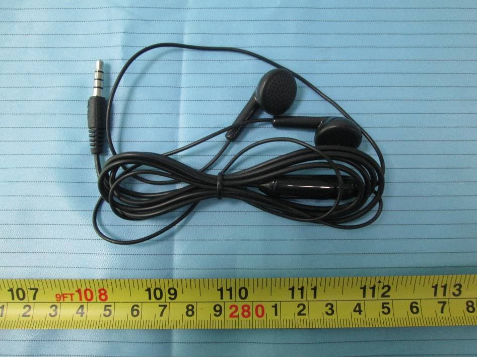
Click to zoom
Application Details
- Equipment Class
- DSS - Part 15 Spread Spectrum Transmitter
- Date of Grant
- Jan 19, 2015
- Application Purpose
- Original Equipment
- Date of Application
- Jan 19, 2015
- Equipment Note
- 3G smartphone
- Frequency Range
- 2402.00000000 - 2480.00000000
- Company
- Collage Investments LLC.
- Country
- United States
Documents & Files
Document Text
Text extracted from the exhibit documents filed with the FCC. Open a document above to read the original.
Users Manual
1 2 Table of Contents 1.Foreword .......................................................... 3 2.Getting to know your touch phone ................. 6 3.Starting up the device ...................................... 7 4.Introduce the basic phone function ................ 9 5.Technical Specifications ................................ 16 6.SAR..................................... ............................. 17 3 1. Foreword Safety In order to ensure the phone is used safely and correctly, please read the precautions below carefully before use. 1.1 General precaution ·Your phone is only suitable for the battery and charger approved by our company or else it may cause the battery to leak, overheat, explode or even catch fire. ·Do not knock, vibrate or throw the phone heavily to avoid malfunction, fire, overheating, explosion or fire. ·If there are abnormal phenomena, like temperature rising, color change or distortion during the usage, charging or storage of the battery, please stop using it and replace it with a new battery. ·It may burn the skin if liquid in the battery leaks onto skin or clothes. If this happens please flush with plenty of clean water immediately and go to a hospital at once. ·Please keep the battery away from fire to avoid fire and explosion if the battery leaks or emits a strange smell. ·Do not place expose the battery to moisture or it may cause overheating, fumes and corrosion. 4 ·Do not use or place the battery under direct sunlight, or in hot places, it may cause leakage and overheating, thus reducing performance and shortening the lifespan. ·Do not charge the battery for over 24 hours continuously. ·Use careful with the earphone maybe possible excessive sound pressure from earphones and headphones can cause hearing loss. 1.2 Precaution for the use of charger ·Do not cause short circuit to the charger, or it may cause electric shock, fumes and damage to the charger. ·Do not use the charger if the power wire is broken, or it may cause fire and electric shock. ·Please remove accumulated dust on the power plug. ·Do not put water containers next to the power supply to avoid overheating, fire, electric shock and malfunction in case they come into contact. ·Do not disassemble or tamper with the charger or it may cause personal injury, electric shock, fire and the damage of the charger. ·Do not use the charger in places of high humidity, like 5 bathrooms, or it may cause electric shock, fire and damage of charger. ·Do not touch the charger, power cord or power plug with wet hands or it can cause electric shock. ·Do not put heavy objects on the power cord or change the power cord or it may cause electric shock and fire. ·Please unplug the power socket before cleaning and maintenance. ·Please hold the charger to unplug the socket as pulling the power cord may damage the power wire and cause electric shock and fire. 1.3 Cleaning and maintenance ·As the phone, battery and charger are not waterproof, do not use them in places of high humidity and avoid them being wet by rain. ·Please clean the battery and charger with a soft dry cloth. ·Never use alcohol, thinner or solutions, like benzene, to wipe the phone. ·Dirty sockets can cause poor contact and power down, and even make recharging unavailable. So, please clean them 6 periodically. 1.4 Common Precaution Mobile Phone: ·Please use the phone in an environment with temperature between -20°C- 45°Cand humidity of <75%. ·Please use the phone far away from regular telephones, TV sets, radio sets and office automation equipment, to avoid affecting the normal use of these equipments and mobile phone. Battery: ·Store the battery in cool and ventilated place without direct sunlight. ·The battery has a limited lifespan. The usage of battery will be shortened progressively due to frequent charging. Once the battery is out of use, it means that its lifespan has ended, and you will need to replace it with an approved new battery. ·Do not dispose of old batteries as household waste. Give them to specified disposal places and follow any stipulated instructions for disposal. CAUTION: RISK OF EXPLOSION IF BATTERY IS REPLACED BY AN INCORRECT TYPE.DISPOSE OF USED BATTERIES 7 ACCORDING TO THE INSTRUCYIONS. Charger: ·Do not charge under following conditions: -- Places with direct sunlight -- Places with ambient temperature less than 0°C or over 40°C, wet or dusty places with strong vibrations (it may cause malfunction) -- Places near electrical appliances (it may affect the image and sound) like TV set, radio, etc -- Adapter shall be installed near the equipment and shall be easily accessible. The plug considered as disconnect device of adapter 8 2. Getting to know your LIKUID L-1 FLYER 1) Handset 2) Receiver 3) LCD display 4) Button menu/home/back 5) Touch Panel 6) Power button 7) Camera 8) Flash 9) Battery cover 10) Speaker 11) Volume button 12) Headphone Jack (Jack3.5)Spearker 13) Micro USB 9 3. Starting up the device To remove the back cover ·Make sure your device is turned off. ·Firmly hold the device with the front panel facing down. ·Slide your finger into the groove at the top of the phone and gently pull open the back cover. To install the SIM card ·Remove the battery if it is installed. ·Locate the SIM card slot, and then insert the SIM card with its gold contacts facing down and its cut-off corner facing out of the card slot as shown in the diagram. ·Slide the SIM card completely into the slot (See picture1). Note: The phone can support two SIM cards. The SIM card slot # 1 will support 3G and a 2G network. The SIM card slot #2, only support 2G network operation. To install a memory card To have additional storage for your images, videos, music and files, you can purchase a memory card and install it in your device. Locate the memory card slot on the upper part of the exposed 10 right panel. Insert the memory card into the slot with its gold contacts facing down until it clicks into place (See picture2). P 1 P 2 To install the battery Ali…
Text truncated - open the document above for the full version.
Block Diagram
Block diagram MTK6572 LCD SPK KEYPAD MIC CAMERA SIM1 SIM2 Transceiver WLAN+BT+ FM Touchpad VIB FLASH WCDMA W850/1900 GSM RF 850/900/1800/1900 ANT ANT Clock26MHZ
External Photos
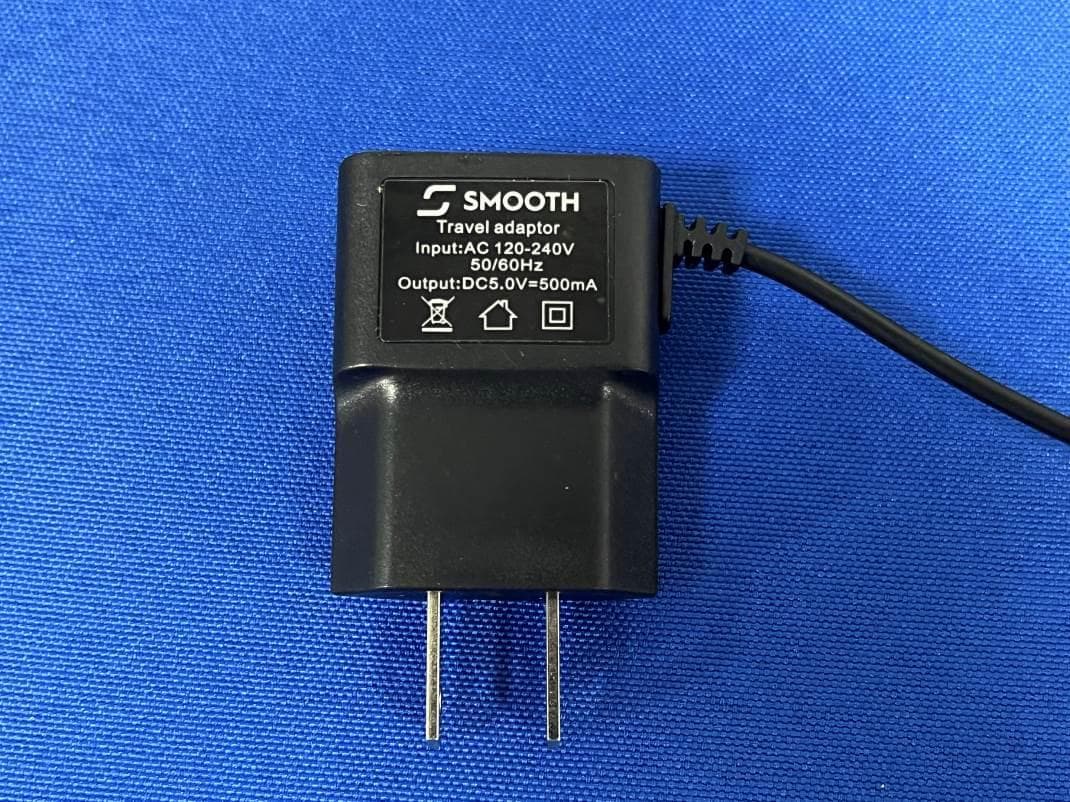
EXHIBIT B - EUT EXTERNAL PHOTOGRAPHS EUT – All View (Red) EUT – Front View (Red) EUT – Rear View (Red) EUT – Top View (Red) EUT – Bottom View (Red) EUT – Left Side View (Red) EUT – Right Side View (Red) EUT – All View (Yellow) EUT – Front View (Yellow) c EUT – Rear View (Yellow) EUT – Top View (Yellow) EUT – Bottom View (Yellow) EUT – Left Side View (Yellow) EUT – Right Side View (Yellow) EUT –Earphone View EUT –Adapter View EUT –Adapter Lable View
ID Label/Location Info
EXHIBIT A - FCC ID LABEL AND LOCATION FCC ID Label FCC ID Label Location Information The label shown shall be permanently affixed at a conspicuous location on the device and be readily visible to the user at the time purchase (Labeling requirements per 2.925)
Internal Photos
EXHIBIT C - EUT INTERNAL PHOTOGRAPHS EUT –Battery off View (Red) EUT –Battery off View (Yellow) GPS Antenna BT/WIFI Antenna GSM/WCDMA Antenna EUT –Cover off View 1 EUT –Cover off View 2 EUT – Main Board Top View EUT – Main Board Bottom View EUT – Main Board Bottom Shielding off View EUT – Connect Board Top View EUT – Connect Board Bottom View EUT –Battery View EUT –Battery Lable View
Operational Description
General Technical Description 1. Scope This document shows and provides the more detail information about the platform we used. The basic description for the Baseband and RF section are also included. 2. System Block Diagram Figure 1 System Overview 3. RF Module 3.1 Transceiver (MT6166) 4. Baseband (MT6572) MT6572 integrates a mixed-signal baseband front-end in order to provide a radio interface with flexibility for efficient customization. It build in gain/offset calibration mechanisms and filters with programmable coefficients for comprehensive compatibility control on RF modules. MT6572 achieves great MODEM performance by utilizing a high resolution A/D converter in the RF downlink path. LCD Antenna transceiver SPK KEYPAD MIC CAMERA VIB WIFI/BT/FM/GPS MT6572 CPU SIM2 FLASH SIM1 Touchpad Battery WCDMA/GSM 5. BT+WIFI+GPS (MT6627) MT6627 is a four-in-one chip, providing the WIFI/BT/GPS features.
Schematics
DCXO+32K XO DCXO+32K-LESS 0 (GND) DCXO_32K_EN 11 3 RF 1(VIO18) 1(VTCXO28) 1(VTCXO28) 1(VTCXO28) 1(VIO18) XMODE VXODIG 0.47UF 2KOHM VRF18-1 VIO18 VIO18_PMU R303 986 7 42 1 105 RFBLN2012090BM5T25 B39212B8558P810 U303 B39941B8515P810B39202B8078P810 CLK1_BB CLK2_WCN 0OHM R309 C305 VTCXO_PMU 0.47UF 0OHM L317 N/A L315 2.7NH 33PF W_B1_TRX L301 5.6NH 4 U306 RX_HBRX_LB 33PF N/A GND_AUXADC L320 2.2NH 0.47UF C333 1UF 3 R322 C303 1 R342 C302 VRF18-1 R326 C351 C301 VTCXO_PMU C312 W_PA_B1_OUT L312 33PF XMODE NA 1 R329 C304 R325 2 1UF L313 W_B2_TRX N/A L326 N/A NA R3070OHM 0.47UF 0OHM NA 0OHM R324 7M26000028 R308 100KOHM 1 C355 N/A C306 R306 1 2 L332 L333 1.5NH 12 N/A N/A L316 C314 L306 W_PA_B2_OUT 33PF VRF18-1 2 C310 L325 33PF L233 5.6NH C31633PF L321 C317 33PF 2 2.2NH N/A 1 L318 C311 33PF VXODIG NA R323 VIO18VTCXO_PMUVIO18VTCXO_PMU 0OHM 0OHM VTCXO_PMU R334 DCXO_32K_EN R333 0OHMR332 VRF18-1 3 U305 CLK4_AUDIO K4 K3 L4 K5 L5 B7 E7 H6 D7 L2 A8 A9 A10 A5 B5 A6 D8 E4 F1E1 B8 E3 C3 C2 C7 C4 E6 C6 D6 G8 H10 A2 F3G3 B11 J8 B6 B3 C1D1J3 E8 D3 B4 H8 J1 G6 D11 A11 H2 L10K11 J10J11 L11 F11F10 J9 H9 F6 J5 F8 A3 C9 J2 L8 K6 L7 K7 J6 G2F2 K1L1 G4 H3 B1A1 K9 K10 K8 MT6166 U301 D4 K2 G1F4 F5 C5 E5 D5 H4 J4 DCXO_32K_EN SRCLKENASRCLKENA DCXO_32K XMODE VXODIG RX_BBIPRX_BBINRX_BBQPRX_BBQN BSI_A_EN BSI_A_CLK BSI_A_DAT0 TX_BBIPTX_BBINTX_BBQPTX_BBQNTXBPI BSI_A_DAT2BSI_A_DAT1 GGE_TX_HB W_PA_LB_IN GGE_TX_LB PDET L305 C315 N/A 10NH27NH 33PF 33PF C313 N/A L33110NH 12 NA R305 AUXADC_REFAUXADC_TSX 0OHM B10 C8 J7 C325 0.47UF C10 G11G10 0.47UF E10C11D10 G9F9E9D9 W_PA_B1_INW_PA_B2_IN 22NH L328 33PF L329 C353 U308 C352 U302 W_PA_LB_OUT W_LB_TRX C335 N/A L302 2 1.5NH 10NHL330 33NH L303 MODEL: SIZE:A3 AEON CORPORATION AEON CORPORATION TITLE: DRAWING NO.: CHECKED VERSION: SHEET OF DRAWN A BC E F GH 5 1 2 3 4 6 7 8 9 D THIS DOCUMENT CONTAINS INFORMATION PROPRIETARY TO AEON CORPORATION (AEON), USE OR DISCLOSURE WITHOUT THE WRITTEN PERMISSION OF AN OFFICER OF AEON IS EXPRESSLY FORBIDDEN. RX0|BALANCEDRX1|BALANCED ANTENNA GND0GND4GND3GND2GND1 TX|UNBALANCEDRX0|BALANCEDRX1|BALANCED ANTENNA GND0GND4GND3GND2GND1 TX|UNBALANCEDRX0|BALANCEDRX1|BALANCED ANTENNA GND0GND4GND3GND2GND1 TX|UNBALANCED DET GND GND GND GND GND GND GND VTXHF 2GLB_TX 3GL5_TX 3GH2_TX 3GH1_TX 2GHB_TX 3GB8_RXN 3GB8_RXP 3GB2_RXN 3GB2_RXP 3GB5_RXN 3GB5_RXP 3GB1_RXN 3GB1_RXP GND GND GND GND GND GNDGNDGNDGNDBSI_DATA1BSI_DATA2TST1TST2RCALTXBPIVTXLFTXVCO_MON 3GTX_QN3GTX_QP3GTX_IN3GTX_IP V28TMEAS DETGNDGNDGNDGNDGNDGNDGND GND GND GND GND GND GND BSI_DATA0 BSI_CLK BSI_EN RX_QN RX_QP RX_IN RX_IP VRXLF VXODIG AVDD_VIO18 XMODE OUT32K XO1 XO2 XO4 GND GND GND GND GND GND GNDGNDGNDGNDXO3 CLK_SEL EN_BB 32K_EN VTCXO28 XTAL2 XTAL1 RFVCO_MON VRXHF HB_RXNHB_RXPLB_RXNLB_RXP B40_RXNB40_RXP GNDGNDGNDGNDGNDGND GND_3 UNBALANCED_PORT_HBUNBALANCED_PORT_LB GND_2 GND_5 GND_10 BALANCED_PORT_LB_9BALANCED_PORT_LB_8BALANCED_PORT_HB_6BALANCED_PORT_HB_7 CRYSTAL_26M GND OUT GND IN 13 RF 4 NA R429 0OHM R426 R4250OHM 818000276 SKY77590 C463 0.1UF GGE_TX_LB W_PA_B1_OUT W_PA_B2_OUT 0OHM R493 R420 C431 W_PA_B1_IN VBAT N/A C470 56PF W_PA_LB_INTD_GSM_PA_ENABLE 47UF C405 R401 C401 22PF U401 N/A 0OHM 56PF C402 NA R406 0OHM NA W_PA_LB_OUT VC5348 7 3 1011 9 U402 2 6 5 1 8 VPA_PMU 22PF 22PF 2.2UF VC5342 11 8 10 U408 2 3 45 1 7 69 U403 3 2 1 45 11 69 7 10 8 22PF 0.1UF C429 22PF VPA_PMU C423 0.1UF C440 R497 R4170OHM 18PF W_PA_B2_IN L402 W_PA_B2_ON 33PF W_PA_B1_ON 220PF 2.2UF C496 100PF R424 NA C422 NA R492 C421 51OHM 0OHM 0OHM R494 C439 36OHM 27.4OHM N/A NA N/A C434 27.4OHM R498 VM1VM0VBATVM1VM0 PDET R403 C419 0.1UF 220PF C415 VBAT 2.2UF R418 C428 C432 N/A C438 R415 R414 N/A C453 C430 N/A C427 220PF VM0VM1 VPA_PMU VC5341 0OHM C420 C412 R471 C414 2.2UF C425 C424 W_PA_LB_ON NA R405 R499 24KOHM C403 220PF R412 10KOHM VAPC1 6PF C407 22PF C406 1 2 VBAT C408 R4070OHM R411 1KOHM R409 1KOHM R408 1KOHM 1KOHM R410 ASM_VC1ASM_VC2ASM_VC0 R402 NA GGE_TX_HB W_B1_TRX 4 W_B2_TRX R462 0OHMR428 ANT402 GA0000110-1207-BGA0000110-1207-BGA0000110-1207-B ANT401 C462 N/A W_LB_TRX RX_HBRX_LB XJ402 ANT403 NA R427 R430 NA MODEL: SIZE:A3 AEON CORPORATION AEON CORPORATION TITLE: DRAWING NO.: CHECKED VERSION: SHEET OF DRAWN A BC E F GH 5 1 2 3 4 6 7 8 9 D THIS DOCUMENT CONTAINS INFORMATION PROPRIETARY TO AEON CORPORATION (AEON), USE OR DISCLOSURE WITHOUT THE WRITTEN PERMISSION OF AN OFFICER OF AEON IS EXPRESSLY FORBIDDEN. VENVMODE1VMODE2|NCRFINVBATT GND_PAD GND CPLOUT CPLIN VCC RFOUT VENVMODE1VMODE2|NCRFINVBATT GND_PAD GND CPLOUT CPLIN VCC RFOUT AAA ANTOUT GND1 ANTIN GND2 GND3 GND4 GNDGNDANT TRX6TRX5TRX4 TRX3 TRX2 TRX1 VRAMP TXEN MODE GND GNDGND VCCVBATTBS1BS2TX_LB_INTX_HB_INGND GND GND GND GND GND GND GND VENVMODE1VMODE2|NCRFINVBATT GND_PAD GND CPLOUT CPLIN VCC RFOUT DVDD18_LCD DVDD18_MIPIRX DVDD18_MIPITX DVDD18_LCD CLOSE TO BB C101,C102,C105 TO MAIN GND DVDD18_CAM AVDD33_USB AVDD18_USB DVDD18_VIO_3 AVDD28_DAC DVDD18_MC0 DVDD18_VIO_1 DVDD3_MC1 VCCIO_EMI DVDD18_VIO_1 FROM THE BB TO PMIC DVDD18_VIO_2 DVDD18_CAM DVDD18_VIO_3 AVDD18_MD LP_DDR2 20K_OHM TO GND LP_DDR1 NORMAL MODE PMIC_SPI_CS: VCCIO_EMI CAP CLOSE TO BB DVDD18_MC0 CAP CLOSE TO BB AVDD18_AP 11 5 AVDD18_AP NO PULL NORMAL MODE BB OK 120MIL VCCIO_EMI VCCIO_EMI DVDD18_VIO_3 DVDD18_LCD DVDD3_LCD DVDD18_VIO_2 DVDD18_MC0 DVDD18_VIO_1 DO NOT USE THESE GPIO DVDD18_MC0 VCCIO_EMI C503 CLOSE TO BB IC, RECOMMAND < 150MIL 1.2V IO FOR DDR21.8V IO FOR DDR1 OK 4MIL - DEFFERENTIAL - GND SHIELDING DVDD18_VIO_2 IF SINGLE-SIDED SMT, PUT C123 & C124 AROUND MEMORY IF DOUBLE-SIDED SMT, PUT C123& C124 BELOW BB. DIFFERENTIAL 4MIL WITH GOOD SHIELDING AS ENABLE SIGNAL @ EMMC BOOT DVDD18_VIO_3DVDD18_VIO_2 DVDD28_BPI AVDD18_MD AVDD18_MD DVDD18_VIO_3 DVDD18_VIO_3 MT6572U501 A13B12B10A10 A7A8 C12A11D11 W_PA_B2_ON C11 EINT_HPPWM_BL_CTRL EINT_ALPXS EINT_MAGW_PA_LB_ONW_PA_B1_ON B11 EINT_ACC D6C7F9F11G11B8 ASM_VC0ASM_VC1 K21 CAM_HREF Y23 CAM_VREFCAM_DAT7CAM_DAT6CAM_DAT5 Y26AB25 CAM_DAT3CAM_DAT4CAM_DAT1 N26 U21U22 CAM_DAT2CAM_DAT0 1.5KOHM N19R24 MIPI_TDN1MIPI_TDP0 AA25Y22 N14 VCN_1V8_PMU B21F18 0.1UF C1102 CONN_SEN E15 CONN_RSTB WB_CTR…
Text truncated - open the document above for the full version.
Test Report
Note: This test report is prepared for the customer shown above and for the equipment described herein. It may not be duplicated or used in part without prior written consent from Bay Area Compliance Laboratories Corp. FCC PART 15.247 TEST REPORT For Collage Investments LLC. 11437 NW 34 STREET, DORAL, FLORIDA 33178 U.S.A FCC ID: GAO-MAX40 Report Type: Original Report Product Type: 3G smartphone Test En gineer: Haiguo Li Re port Number: RSH141225050-00A Re port Date: 2015-01-08 Reviewed B y: Jimmy Xiao RF En gineer Prepared By: Bay Area Compliance Laboratories Corp. (Shenzhen) 6/F, the 3rd Phase of WanLi Industrial Building ShiHua Road, FuTian Free Trade Zone Shenzhen, Guangdong, China Tel: +86-755-33320018 Fax: +86-755-33320008 www.baclcorp.com.cn Bay Area Compliance Laboratories Corp. (Shenzhen) Report No.: RSH141225050-00A FCC Part 15.247 Page 2 of 62 TABLE OF CONTENTS GENERAL INFORMATION ....................................................................................................................................... 4 PRODUCT DESCRIPTION FOR EQUIPMENT UNDER TEST (EUT) ..................................................................................... 4 OBJECTIVE ................................................................................................................................................................... 4 RELATED SUBMITTAL(S)/GRANT(S) ............................................................................................................................. 4 TEST METHODOLOGY .................................................................................................................................................. 4 TEST FACILITY ............................................................................................................................................................. 5 SYSTEM TEST CONFIGURATION .......................................................................................................................... 6 EXTERNAL I/O CABLE .................................................................................................................................................. 6 BLOCK DIAGRAM OF TEST SETUP ................................................................................................................................ 6 SUMMARY OF TEST RESULTS ............................................................................................................................... 7 FCC §15.247 (i) & §2.1093 – RF EXPOSURE ............................................................................................................ 8 APPLICABLE STANDARD .............................................................................................................................................. 8 FCC §15.203 – ANTENNA REQUIREMENT ............................................................................................................ 9 APPLICABLE STANDARD .............................................................................................................................................. 9 ANTENNA CONNECTOR CONSTRUCTION ...................................................................................................................... 9 FCC §15.207 (a) – AC LINE CONDUCTED EMISSIONS ..................................................................................... 10 APPLICABLE STANDARD ............................................................................................................................................ 10 MEASUREMENT UNCERTAINTY .................................................................................................................................. 10 EUT SETUP ................................................................................................................................................................ 10 EMI TEST RECEIVER SETUP ....................................................................................................................................... 11 TEST PROCEDURE ...................................................................................................................................................... 11 TEST EQUIPMENT LIST AND DETAILS ......................................................................................................................... 11 CORRECTED FACTOR & MARGIN CALCULATION ....................................................................................................... 11 TEST RESULTS SUMMARY .......................................................................................................................................... 12 TEST DATA ................................................................................................................................................................ 12 FCC §15.205, §15.209 & §15.247(d) – RADIATED EMISSIONS ........................................................................... 15 APPLICABLE STANDARD ............................................................................................................................................ 15 MEASUREMENT UNCERTAINTY .................................................................................................................................. 15 EUT SETUP ................................................................................................................................................................ 15 EMI TEST RECEIVER & SPECTRUM ANALYZER SETUP .............................................................................................. 16 TEST PROCEDURE ...................................................................................................................................................... 16 CORRECTED AMPLITUDE & MARGIN CALCULATION ................................................................................................. 17 TEST EQUIPMENT LIST AND DETAILS ..................…
Text truncated - open the document above for the full version.
Test Setup Photos
EXHIBIT D - TEST SETUP PHOTOGRAPHS Conducted Emissions - Front View Conducted Emissions - Side View Radiated Emissions – Front View (30-1000 MHz) Radiated Emissions – Rear View (30-1000 MHz) Radiated Emissions – Front View (1-25 GHz) Radiated Emissions – Rear View (1-25 GHz)
Contact Information
Applicant
Daniel Esteban Gonzalez(Manager)
Test Firm
Bay Area Compliance Laboratory Corp. (Shenzhen)John Chan
Technical Specifications
| # | Rule Parts | Frequency Range | Power Output |
|---|---|---|---|
| 1 | 15C | 2.40 GHz - 2.48 GHz | 1.77 mW |
Other Applications from Collage Investments LLC.
GAO-FLIP4G
Nov 30, 2023Mobile Phone
Equipment Class
DTS - Digital Transmission System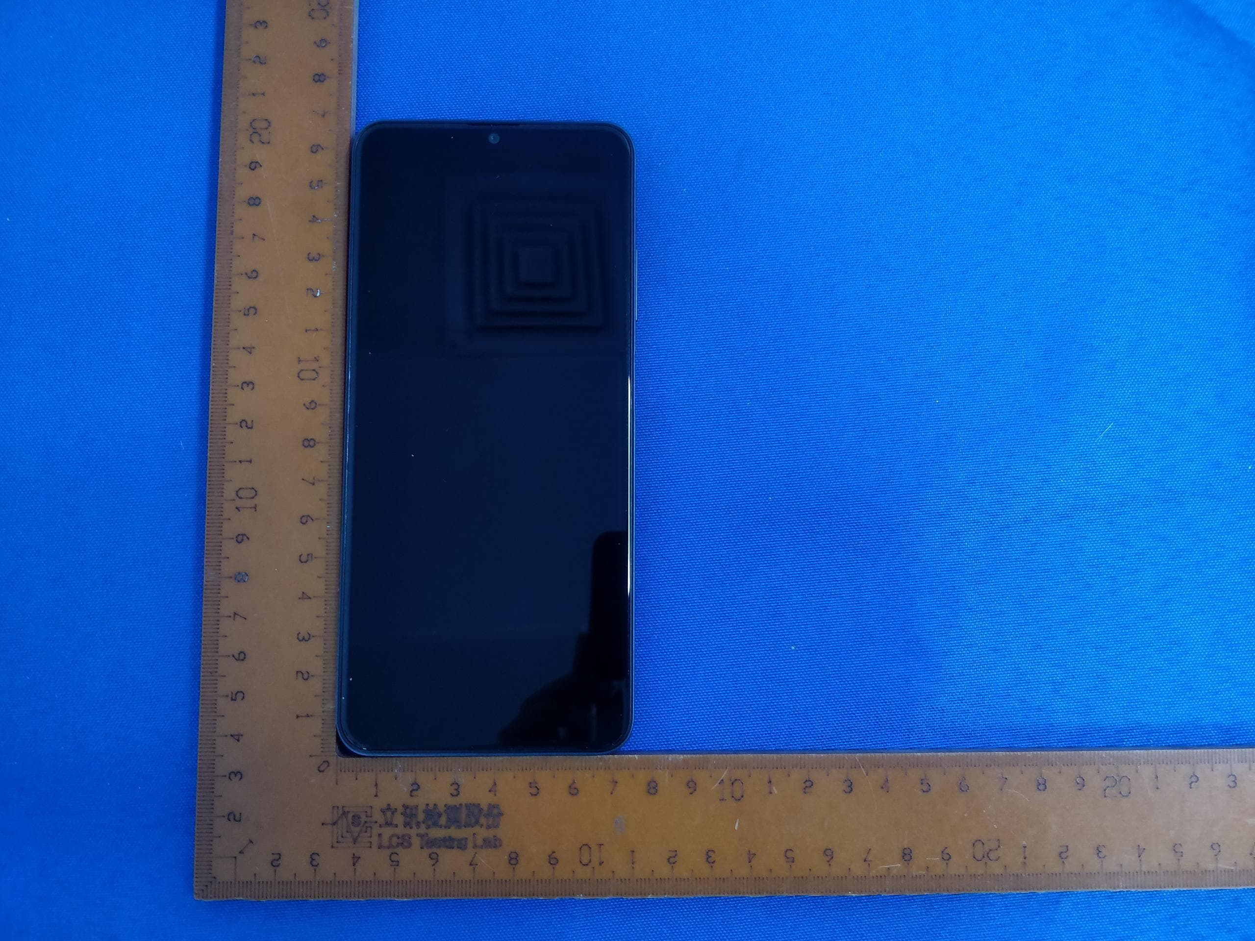
GAO-VISPLU
Jan 30, 2023Smartphone
Equipment Class
DTS - Digital Transmission System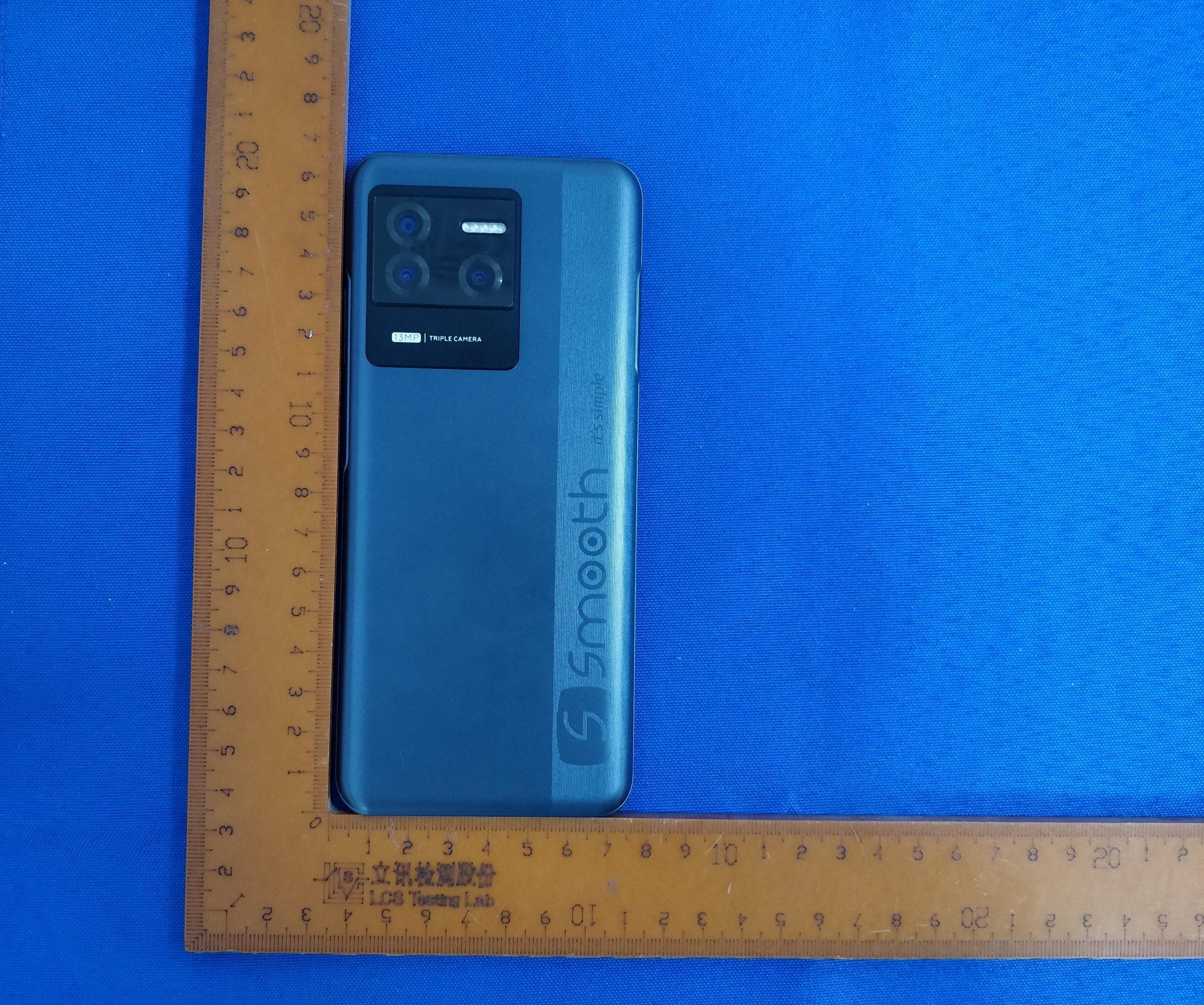
GAO-VISION
Jan 17, 2023Smartphone
Equipment Class
PCE - PCS Licensed Transmitter held to ear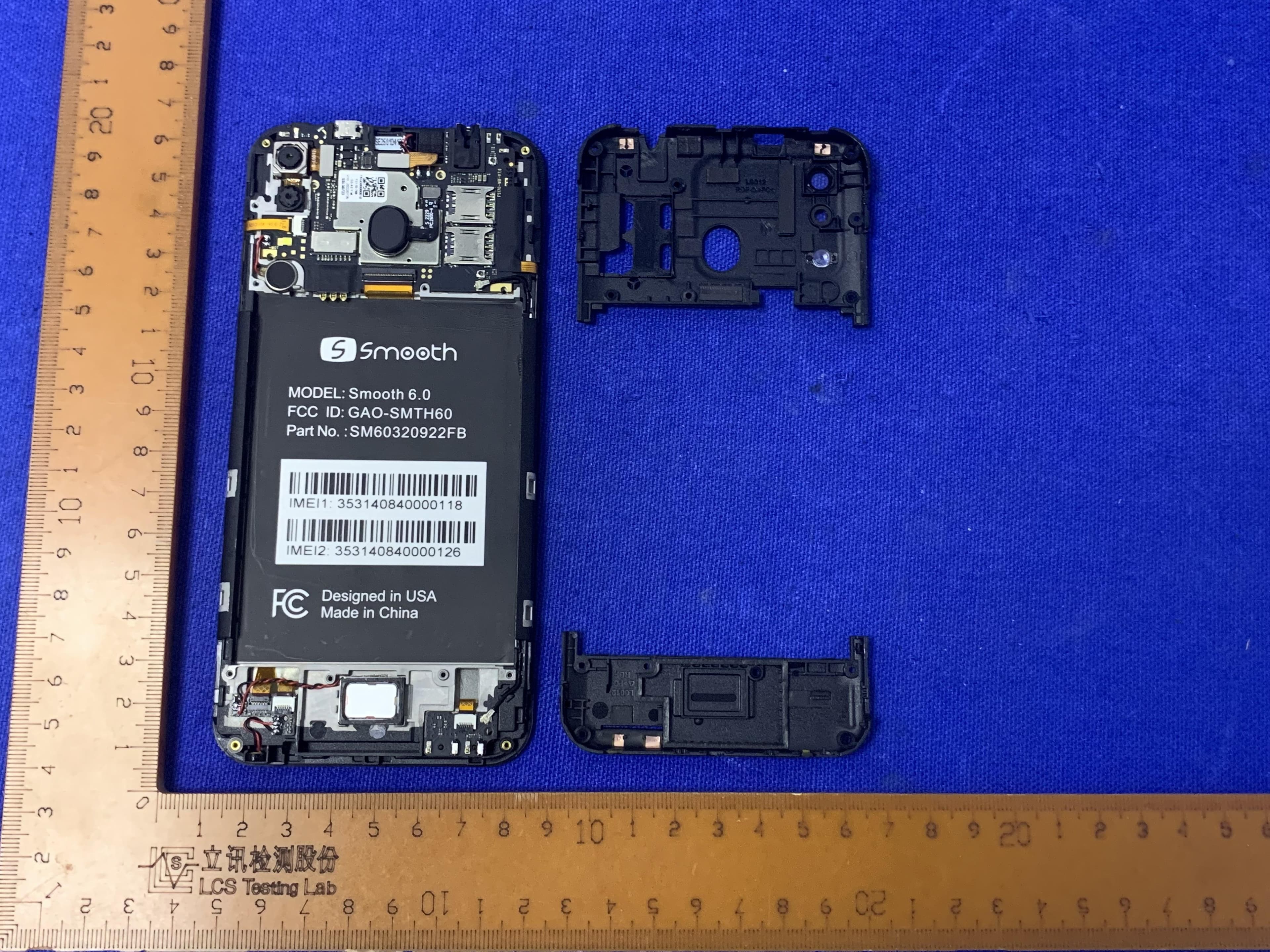
GAO-SMTH60
Oct 13, 2022Smart phone
Equipment Class
DSS - Part 15 Spread Spectrum Transmitter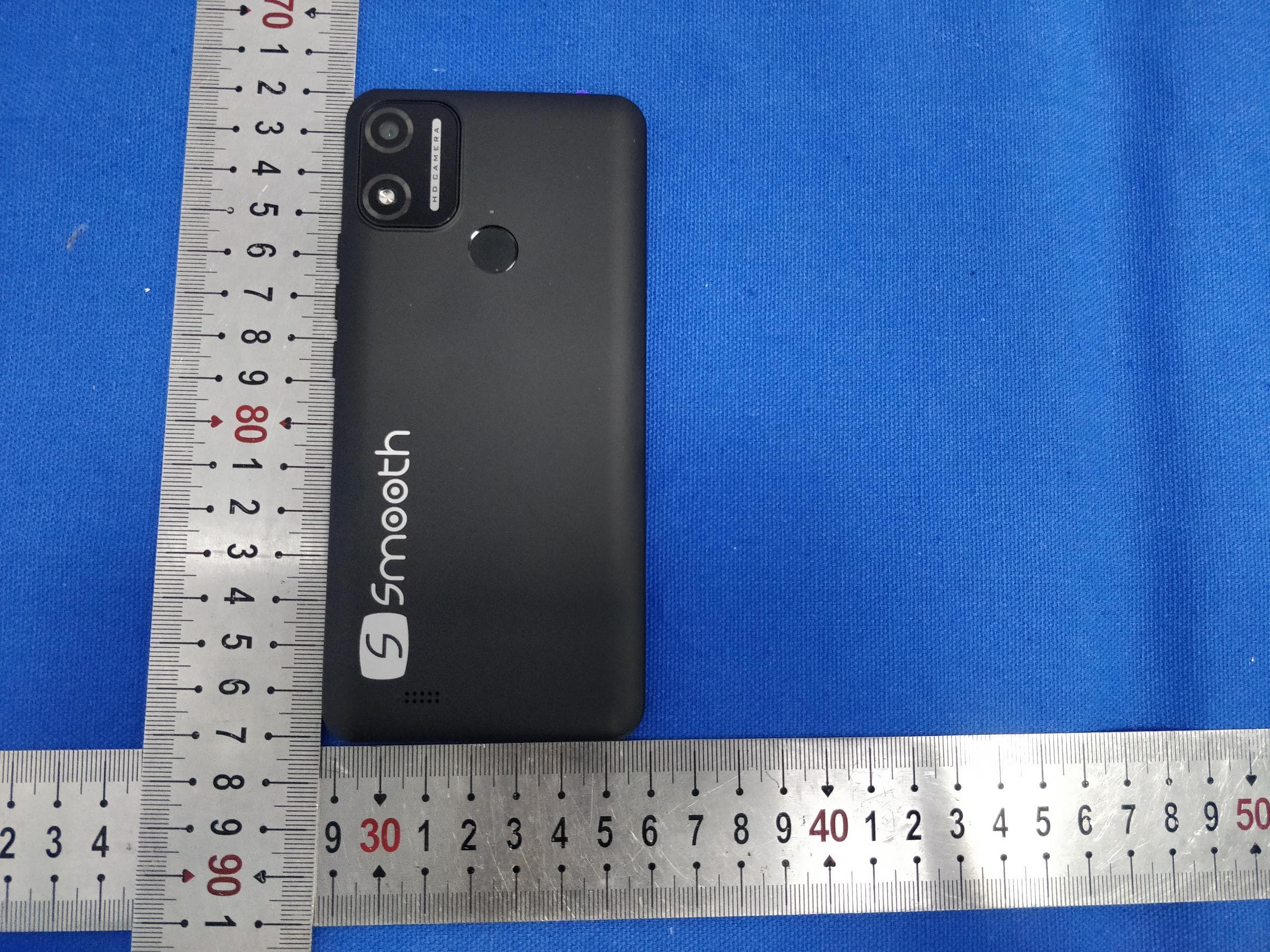
GAO-55MAX22
Jun 07, 2022Smart phone
Equipment Class
PCE - PCS Licensed Transmitter held to ear