HEOE3240CDMA 800MHz Mobile Phone
GFIVE MOBILE FZE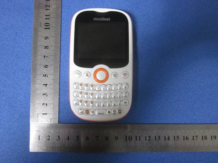
Click to zoom
Application Details
- Equipment Class
- TNE - Licensed Non-Broadcast Transmitter Held to Ear
- Date of Grant
- Dec 17, 2013
- Application Purpose
- Original Equipment
- Date of Application
- Dec 17, 2013
- Equipment Note
- CDMA 800MHz Mobile Phone
- Frequency Range
- 824.70000000 - 848.31000000
- Company
- GFIVE MOBILE FZE
- Country
- China
Documents & Files
Document Text
Text extracted from the exhibit documents filed with the FCC. Open a document above to read the original.
Users Manual
·Copyright©2013 Movilnet Telecommunications. All Rights Reserved Reproduction, transfer, distribution or storage of part or all of the contents in this document in any form without the prior written permission as Movilnet Telecommunications.. Statement The contents of this manual maybe different wi th the cell phone please according to the cell phone. Movilnet Telecommunications. reserves the right to revise this document or withdraw it at any time without prior notice. GFIVE MOBILE FZE Unit 1, 16/F, Cable TV Tower, 9 Hoi Shi ng Road, Tusen Wan, N.T., Hong Kong, China I Safety Precautions Please read these simple guidelines. Not following them may be dangerous or illegal. For further information, see the secti on of “Warnings and Precautions”. Do not switch the phone on when Mobile Phone use is prohibited or when it may cause interference or danger. Do not place your phone and its accessories in containers with strong electromagnetic field. Obey all local laws. Always keep your hands free to operate the vehicle while driving. Your first consideration while driving should be road safety. Hospitals or health care facilities may be using equipment that could be sensitive to external radio frequency energy. Follow any regulations or rules in force. II Do not use the phone at a refueling point. Do not use near fuel or chemicals. Follow any restrictions. Wireless devices can cause interference in aircraft. Keep the phone and all its parts, includi ng accessories, out of the reach of small children. Use only approved batteries and charger s. Disconnect the charger from the power source when it is not in use. Do not leave the battery connected to a charger for more than a week, since overcharging may shorten its lift. Only qualified personnel should service the phone or install the phone in a vehicle. Faulty installation or service may be dangerous and may invalidate any warranty applicable to the device. i Contents 1 Getting to Know Your Phone.................................................................. 1 Basic specification...........................................................................................................1 Mobile phone appearance..............................................................................................3 The appearance of the mobile phone and introductions ...............................................4 T ‐ Flash Card slot showing picture ..................................................................................7 Icon bar.........................................................................................................................10 Text input method.........................................................................................................14 Change the input method.............................................................................................14 Shortcut Menu of the Standby Mode...........................................................................14 Switching on/off............................................................................................................16 ii 2 Making phone call............................................................................... 17 Making phone call by dialing number...........................................................................17 Making phone call using contacts.................................................................................17 Making phone call using recent all calls........................................................................17 Making phone call using speed dial..............................................................................18 Making a conference call ..............................................................................................18 3 Answering the call............................................................................... 19 Answer or silence an incoming call...............................................................................19 Adjust the receiver volume...........................................................................................19 Answer a call with the keypad locked ...........................................................................19 Operations during a call................................................................................................19 Keypad lock...................................................................................................................20 Emergency calls.............................................................................................................21 4 Contacts...................................................................................... 21 List........................................................................................................................... ......21 View ........................................................................................................................... ...22 iii Edit........................................................................................................................... .....22 Options ........................................................................................................................ .22 Groups settings.............................................................................................................23 Speed dial......................................................................................................................23 5 Messages................................................................................... 24 Messages....................................................................................................................... 24 MMS............................................................................................................................ ..27 Voice Mail ....................................................................................…
Text truncated - open the document above for the full version.
Cover Letter(s)
GFIVE MOBILE FZE Unit 1, 16/F, Cable TV Tower, 9 Hoi Shing Road, Tusen Wan, N.T., Hong Kong, China Tel: 00852- 24169300 Fax: 00852- 24169302 DOC ATTESTATION LETTER FCC ID: HEOE3240 Date: Dec. 12, 2013 Federal Communications Commission Authorization and Evaluation Division 7435 Oakland Mills Road Columbia, MD 21046 To whom it may concern: I, the undersigned, hereby attest to the fact that I will apply the Declaration of Conformity procedure to the receiver operate at frequencies from 30-960 MHz device. I understand the following FCC requirements: 1. Devices subject to the DoC procedure are required to be tested to show compliance with the FCC technical regulations by a recognized accredited testing laboratory. The testing laboratory must be accredited by a Commission approved accreditation body or designated under the terms of a government-to-government Mutual Recognition Agreement (MRA). A listing of those accredited testing laboratories that have been recognized by the Commission is published on the FCC Webpage: https://apps.fcc.gov/oetcf/eas/reports/TestFirmSearch.cfm (Select the "accredited" option to search for FCC recognized accredited test firms.)\ 2. Test facilities located in countries, where the U.S. does not have an operational Telcom MRA are not recognized by the FCC to test for the DoC procedure. 3. Pt 2.1077 contains the list of information that must be included in the Declaration of Conformity, which must be supplied with each product sold. The DoC compliance info shall be included in the User’s Manual or as a separate sheet. The info must contain the name, address, and phone number of the responsible party, which must be located within the United States. According to 2.909(c)(2), the responsible party is either the Manufacturer or if the product is imported the Importer. Sincerely, ------------------------------ Jerry Tang/ Operator Director
Cover Letter(s)
GFIVE MOBILE FZE Unit 1, 16/F, Cable TV Tower, 9 Hoi Shing Road, Tusen Wan, N.T., Hong Kong, China Tel: 00852- 24169300 Fax: 00852- 24169302 AGENCY AUTHORIZATION LETTER FCC ID: HEOE3240 Date: Dec. 12, 2013 Federal Communications Commission Authorization and Evaluation Division 7435 Oakland Mills Road Columbia, MD 21046 To whom it may concern: We, the undersigned, hereby authorize Shenzhen CTL Electromagnetic Technology Co., Ltd.(MR. Tracy Qi) on our behalf, to apply to the Federal Communications Commission on our equipment. Any and all acts carried out by Shenzhen CTL Electromagnetic Technology Co., Ltd. (MR. Tracy Qi) on our behalf shall have the same effect as acts of our own. This authorization expires on Dec. 11, 2014. This is to advise that we are in full compliance with the Anti-Drug Abuse Act. We, GFIVE MOBILE FZE are not subject to a denial of federal benefits pursuant to Section 5301 of the Anti-Drug Act of 1988, 21 USC853a, and no party to the application is subject to a denial of federal benefits pursuant to that section. Sincerely, ------------------------------ Jerry Tang/ Operator Director
Cover Letter(s)
QuieTek Corporation Page 1 of 1 Test Lab Attestation Letter Date of Test: 12/02/2013 Applicant Name: GFIVE MOBILE FZE FCC Id: HEOE3240 Reviewed By: Jame Yuan Title: Manager Email Address: Jameyuan @quietek.com.cn Phone No.: +86‐512‐62515088‐5160 Statement of Compliance: QuieTek Corporation Suzhou EMC Laboratory declares that this Unit has been tested in accordance with the test method identified in this test report and that we observed it being tested. It also declares that the Unit complies with the relevant limits. All instrumentation and accessories used to test this unit for compliance to the indicated test method are calibrated regularly in accordance with ISO 17025:2005 requirements by laboratories accredited by A2LA, NVLAP, or ACLAS for the measurement parameters. The measurements were made at: QuieTek Corporation Suzhou EMC Laboratory No.99 Hongye Rd., Suzhou Industrial Park Loufeng Hi‐Tech Development Zone., Suzhou, China Test Lab Witness‐ Approved By: Jame Yuan Title of Witness: Manager Email Address: [email protected] Phone No.: +86‐512‐62515088‐5160
Cover Letter(s)
深圳市华标检测技术服务有限公司 Bontek Compliance Testing Laboratory Ltd Page 1 of 1 Test Lab Attestation Letter Date of Test: 12/05/2013 Applicant Name: GFIVE MOBILE FZE FCC ID: HEOE3240 Name of Engineer Performing Test: Tracy Qi Statement of Compliance: Bontek Compliance Testing Laboratory Ltd declares that this Unit has been tested in accordance with the test method identified in this test report and that we observed it being tested. It also declares that the Unit complies with the relevant limits. All instrumentation and accessories used to test this unit for compliance to the indicated test method are calibrated regularly in accordance with ISO 17025:2005 requirements by laboratories accredited by A2LA, NVLAP, or ACLAS for the measurement parameters. The measurements were made at: Bontek Compliance Testing Laboratory Ltd 1/F, Block East H‐3, OCT Eastern Ind. Zone, Qiaocheng East Road, Nanshan, Shenzhen, China Test Lab Witness‐ Signature of Test Lab Witness: Full Name, Typed: Kendy Wang Title of Witness: EMC Director Email Address: [email protected] Phone No.: +86‐755‐86337076
ID Label/Location Info
FCC ID Label Information 1. Label location: 2. FCC ID Label: GFIVE CDMA 800MHz Mobile Phone Model: E3240 FCC ID: HEOE3240
ID Label/Location Info
GFIVE MOBILE FZE Unit 1, 16/F, Cable TV Tower, 9 Hoi Shing Road, Tusen Wan, N.T., Hong Kong, China Tel: 00852- 24169300 Fax: 00852- 24169302 Letter for Label Proposal FCC ID: HEOE3240 Dec. 17, 2013 Equipment Authorization Division Office of Engineering and Technology Federal Communications Commission 7435 Oakland Mills Road Columbia, MD 21046 Dear Sirs: GFIVE MOBILE FZE requests acceptance of the labeling proposal described below for transceivers bearing FCC identifier HEOE3240. The subject transceivers are compact handheld models as shown in figure 1, authorized under FCC Part 22/24 for mobile services. Figure 1. Because the majority of the transceiver housing is composed of display, speaker, operating controls, and a removable battery pack, there is extremely limited space available to attach the required label carrying the FCC identifier. Attaching the label to the battery pack is not acceptable because the battery pack is a removable item. For this reason, we propose placing the label carrying the FCC identifier inside the battery compartment as shown in figure 2. GFIVE MOBILE FZE Unit 1, 16/F, Cable TV Tower, 9 Hoi Shing Road, Tusen Wan, N.T., Hong Kong, China Tel: 00852- 24169300 Fax: 00852- 24169302 Proposed Label Location on EUT Figure 2. The consumer packaging for these models includes the battery pack as a separate item, NOT installed on the radio. As such, the FCC identifier will be readily visible to the user before the battery pack is installed and whenever the battery pack is removed or replaced. In this location, the label will also be protected from physical abuse and remain readable for the anticipated life of the device. The consumer packaging for these models is a "gift box" which does not allow the transceiver to be seen at time of purchase. In order to meet the requirements of 47CFR Part 2.925 (d), We will add the FCC identifier "HEOE3240" to the outside of the consumer "gift box" packaging. Sincerely yours, ------------------------------ Jerry Tang/ Operator Director
Operational Description
Operation Description E3240 is based on the Qualcomm QSC6085-1 platform, with the following components. 1. CPU: QSC6085-1-1 2. PA : WS1103-TR1 3. NAND&DDR: MT29C1G12MAVNAJC-6 IT 2.2 Circuit of Functional Unit 2.2.1 Baseband Unit The baseband is made up of CPU, memory and some peripheral drive circuits in the main. CPU integrates multiple processor on-chip: one ARM microprocessor (ARM926EJ-S) and one DSP processor (mDSP). mDSP is dedicated for modem functions and CDMA process. ARM9 offers different interface such as RF interface, UIM card interface, USB interface, I2C interface, UART interface and JTAG interface. 2.2.2 RF Unit The RF circuit of E3240 includes: antenna, RF connector, duplexer, PA, TX SAW filter and RX SAW filter. QSC6085-1 device (adding CDMA2000 diversity and CDMA2000 EV-DO rev. A support) devices. Modulation: QPSK RF transmitter Cellular-CDMA, band class 0: 824 to 849 MHz RF receivers Cellular-CDMA, band class 0: 869 to 894 MHz QSC6085-1 data rate is FL 3.1Mbps / RL 1.8Mbps QSC6085-1 single chip integrates the RF subsystem, which includes RF transmitter, receiver, Frequency synthesizer, and power distribution circuit. The RF subsystem inside E3240 support CDMA800 (BC0), and the transmitter and receiver are zero intermediate frequency (ZIF) architecture, thus those image filter and IF filter for super heterodyne architecture system are not required. VGAs (variable-gain amplifier) in the transmitter and receiver are controlled by baseband circuits. The LO signals for the direct up-converter and direct down-converter are generated by the PLL, and the frequency is variable according to the channel ID. Transmission: The transmit signal is directly up-converted from the baseband to RF, and amplified by the VGA, then amplified by the PA, and finally radiated by the antenna. Receiving: The received signal is fed in through the antenna and duplexer, and is amplified by internal LNA, filtered by balun filter and then directly down-converted from RF to baseband. Before demodulation, the signal should be filtered, amplified and converted from analog signal to digital signal Red: signal to / from antenna; Green: Rx signal; Blue: Tx signal Local oscillation Y502 is a 19.2M+/-10ppm. Power supply 2.2.3 Bluetooth Unit The BTS4025 device is a 0.13 μm CMOS system-on-chip (SoC) with integrated baseband and 2.4 GHz radio for Bluetooth wireless technology applications with enhanced data rates (EDR) up to 3 Mbps. The BTS4025 IC supports both class 2 and class 1 power level transmission without requiring an external power amplifier. The BTS4025 device is intended for use in mobile phone systems and other applications requiring Bluetooth functionality with a pulse coded modulation (PCM) interface, and a host controller interface (HCI) using a UART transport. The BTS4025 has the option to control sleep/wakeup by using either software or hardware. Low power page scan function reduces device power consumption significantly. The BTS4025 offers high levels of performance with increased output power to 6 dBm, and a significant reduction in page scanning current. The device is offered in an ultra-small wafer level chip scale package (WLCSP) with industry standard BGA ball pitch and ball diameter. The package design, along with no requirement for underfill and a small number of external components, reduces the overall footprint and system costs substantially. The hardware and ROM-resident firmware are fully compliant with the Bluetooth V2.1 + EDR specification, including all mandatory and optional features, except for multiple SCO/Esco connections; only one SCO or eSCO connection at a time is supported. The BTS4025 packet traffic arbitration (PTA) coexistence feature provides reliable performance of both the Bluetooth when used in a collocated environment.
Parts List/Tune Up Info
Main Board BOM 1 Main PCBA 1 2 MB1116T200 Main PCB,6layers 1 3 QSC6085-1 QSC6085-1 BASEBAND,QUALCOMM Single Chip,424 CSP 1 U501 5 BTS4025 BTS4025 System-on-ChipBluetooth,,WLCSP36PIN,3.18*2.86*0.6mm 1 U1101 6 WS1103-TR1 RF PA, CDMA 95A/B,CDMA2000-1X/EVD0,8-pin surfacemounting package(3mm*3mm*1.4mm) 1 U205 7 NMI5625 DTV & FM Single-Chip CMOS Receiver IC 1 U1801 8 RDA5802NS FM Tuner,3*3 20pin QFN 1 U1501 9 FAR-D5NC-881M50-M11B SAW duplexer, CDMA cellularband(836.5/881.5MHz),2.5*2.0*0.6mm 1 F101 10 FAR-F5KA-836M50-D4DF-Z SAW Filter for CDMA cellular band Tx(836.5MHz),1.4*1.0*0.5mm,50/50ohm unbalance 1 U201 11 FAR-F5KB-881M50-B4ED-Z SAW Filter for CDMA cellular band Rx(881.5MHz),1.4*1.0*0.5mm,50/100ohm 1 U301 12 LDC18836M20Q-368 Coupler,836MHz 1 U207 13 LFB182G45SG9A293 Bluetooth Band pass filter,2.4G 1 U1102 14 LDA313G0313F-240 Chip Antenna ,2.4G 1 J1201 15 SSP-T7-F(7.0pf,±20ppm) Crystal, 32.768KHz, +/-20ppm, 7pF, 7.0*1. 5*1.4(mm) 1 Y501 16 1XTV19200ACH VCO, 19.2MHz, +2.8V, 3.2*2.5*0.9(mm) 1 Y502 17 7M26000314 Crystal,26Mhz,+/-10 ppm, 8.5pF ,3.2*2.5 1 Y1801 18 7M32000035 Crystal, 32Mhz, +/-15 ppm 1 Y1101 Ref. No. U1001 Description Memory,1Gbit(16bit)NAND FLASH and512Mbit(16bit)DDR,166M,1.8V,107TBGA Package QTY 1 Supplier P/N MT29C1G12MAVNAJC-6 IT Rev . Item 4 19 AW9523BTOR Multi-function I/O Drive,16 bit 1 U1 20 AW8735TQR K class audio amplifier,NCN function,3mm×3mm 20-Pin TQFN 1 U1401 21 XC6221A282MR RF LDO ,high speed,2.8V,SOT23-5 1 U202 22 SGM2019-1.8YN5G/TR LDO,1.8V,SOT23-5 1 U1203 23 ECT818000001 Coxial connector 1 J101 24 99-213UMC-3640661-TR8-T Side View White LEDs (0.8mm) 5 D1601 D1602 D1603 D1604D1701 25 M74VHC1GT50DFT2G CMOS logic Level shifter,3.5ns,SOT-353(Pb-Free) 1 U1103 26 MBT35200MT1G Transistor, PNP , Vcbo=55V, Ic=2A 1 Q601 27 NTS2101PT1G Transister, P channel MOSFET, Vdss=8V, Vgs=8V,Id=1.4A 1 Q602 28 DTC114TET1G Transistor, NPN, Iceo=500nA, Vce=50V 1 Q1401 29 RB520S-30FJTE61 Schottky barrier diode 1 D1605 30 PESD5V0S1BL TVS, bidirectional Esd protection,5V,35pf,SOD882,1.0 x 0.6 x 0.5 mm 1 D1801 31 AVLC18S02015 Chip Varistor, 0402,18V, 15pF 2 R1202 R1306 32 AVLC5S02050 Chip Varistor, 0402, 5.5V, 50pF 29 D1402 R608 R1302 R1401 R1410R1411 R1412 R1420 R1421R1422 R1427 R1428 R1614R1615 R1616 R1617 R1618R1619 R1620 R1621 R1622R1623 R1624 R1625 R1626R1627 R1628 R1629 R1706 33 AIES12U020R2 ESD-Suppressor,12V,0.2pF,0402,for usb protection 2 D1 301 D1302 34 AVRC14S05Q030100R 4-line EMI/ESD,RC Type,14V,30pF,100ohm,0805 2 U1 201 U1202 35 MPL2016S4R7NHT Ind power, 4.7u,+/-30%,2.0*1.6mm 2 L601 L602 36 GZ1005U102TF Chip Ferrite Bead,0402,1000ohm at 100MHz 5 L1405 L1406 L1407 L1801L1802 37 PZ1608U221-1R4TF Chip Ferrite Bead,0603,220ohm at 100MHz 2 L1403 L 1404 38 B30-CY03P-400-000 3PIN,Pitch3.0,Battery connector 1 CN1301 39 USB-MC05-245-002 micro usb,5pin 1 CN1302 40 MSD-QS08-200-000 T-Flash card connector 1 CN1303 41 J35-PT04-470-002 Audio Jack,Ф3.5,SMT 1 CN1401 42 SDNT1005X104F4250FTF NTC Thermisor ,100K, 1% 1 R203 43 SDCL1005C1N5STD(f) ind,1.5n,+/-0.3n,0402 1 L1103 44 SDCL1005C2N7STD(f) ind,2.7n,+/-0.3n,0402 1 L105 45 SDCL1005C3N3STD(f) ind,3.3n,+/-0.3n,0402 1 L102 46 SDCL1005C4N3STD(f) ind,4.3n,+/-0.3n,0402 2 L401 L402 47 SDCL1005C8N2JTD(f) ind,8.2n,+/-5%,0402 1 L103 48 SDCL1005C9N1JTD(f) ind,9.1n,+/-5%,0402 1 L1803 49 SDCL1005C10NJTD(f) ind,10n,+/-5%,0402 1 L303 50 SDCL1005C12NJTD(f) ind,12n,+/-5%,0402 1 L301 51 SDCL1005CR10JTD(f) ind,100n,+/-5%,0402 2 L1401 L1402 52 SDCL1608CR15JTD(f) ind,150n,+/-5%,0603 2 L1805 L1806 53 C0402C0G1R0B500NT cap,1p,+/-0.1p,50V,C0G,0402 1 C1812 54 C0402C0G1R5B500NT cap.1.5pf,+/-0.1pf,50V,C0G,0402 1 C402 55 C0402C0G2R7B500NT cap,2.7p,+/-0.1p,50V,C0G,0402 1 C101 56 C0402C0G6R8C500NT cap,6.8p,+/-0.25p,50V,C0G,0402 3 C1106 C1819 C18 20 57 C0402C0G8R2D500NT cap,8.2p,+/-0.5p,50V,C0G,0402 2 C1101 C1102 58 C0402C0G120J500NT cap,12p,+/-5%,50V,C0G,0402 2 C501 C502 59 C0402C0G180J500NT cap,18p,+/-5%,50V,C0G,0402 2 C1110 C1112 60 C0402C0G200J500NT cap,20p,+/-5%,50V,C0G,0402 1 C301 61 C0402C0G220J500NT cap,22p,+/-5%,50V,C0G,0402 1 C1813 62 C0402C0G270J500NT cap,27p,+/-5%,50V,C0G,0402 3 C1425 C1426 C1818 63 C0402C0G330J500NT cap,33p,+/-5%,50V,C0G,0402 6 C1203 C1206 C1207 C1208C1209 C1404 64 C0402C0G820J500NT cap,82p,+/-5%,50V,C0G,0402 2 C401 C403 65 C0402C0G101J500NT cap,100p,+/-5%,50V,C0G,0402 18 C102 C201 C204 C207 C216C409 C512 C625 C627 C1201C1202 C1204 C1205 C1301C1401 C1403 C1424 C1602 66 C0402X7R221K500NT cap,220p,+/-10%,50V,X7R,0402 2 C407 C1407 67 C0402X7R102K500NT cap,1n,+/-10%,50V,X7R,0402 13 C205 C304 C504 C601 C604C622 C1412 C1413 C1416 C1417C1418 C1419 C1420 68 C0402X7R332K500NT cap,3.3n,+/-10%,50V,X7R,0402 1 C408 69 C0402X7R472K500NT cap,4.7n,+/-10%,50V,X7R,0402 2 C308 C310 70 C0402X7R562K250NT cap,5.6n,+/-10%,25V,X7R,0402 1 C1817 71 C0402X7R103K250NT cap,10n,+/-10%,25V,X7R,0402 3 C203 C507 C1228 72 C0402X7R223K160NT cap,22n,+/-10%,16V,X7R,0402 4 C1405 C1406 C1821 C1822 73 C0402X7R333K160NT cap,33n,+/-10%,16V,X7R,0402 1 C506 74 C0402X7R683K100NT cap,68n,+/-10%,10V,X7R,0402 1 C311 75 C0402X7R823K100NT cap,82n,+/-10%,10V,X7R,0402 1 C309 76 C0402X5R104K100NT cap,100n,+/-10%,10V,X5R,0402 29 C208 C303 C503 C505 C508C509 C510 C511 C513 C603C710 C711 C712 C713 C714C716 C717 C1001 C1114 C1211C1302 C1423 C1601 C1603C1802 C1803 C1805 C1806C1807 77 C0402X5R224K6R3NT cap,220n,+/-10%,6.3V,X5R,0402 1 C209 78 C0402X5R105K6R3NT cap,1.0u,+/-10%,6.3V,X5R,0402 26 C613 C619 C621 C701 C702C703 C704 C705 C706 C707C708 C709 C715 C1103 C1104C1105 C1107 C1210 C1226C1227 C1422 C1801 C1804C1808 C1825 C1826 79 C0402X5R225M6R3NT cap,2.2u,+/-20%,6.3V,X5R,0402 7 C610 C611 C612 C616 C618C620 C628 80 C0603X5R225K6R3NT cap,2.2u,+/-10%,6.3V,X5R,0603 1 C623 81 C0603X5R475K6R3NT cap,4.7u,+/-10%,6.3V,X5R,0603 9 C206 C602 C605 C607 C614C615 C617 C624 C1410 82 C0603X5R106M6R3NT cap,10u,+/-20%,6.3V,X5R,0603 1 C1408 83 C0805X5R106K6R3NTM cap,10u,+/-20%,6.3V,X5R,0805 1 C606 84 C0805X5R226M6R3NTM cap,22u,+/-20%,6.3V,X5R,0805 3 C626 C1414 C1415 85 C0805X5R106K100NTM cap,10u,+/-10%,10V,X5R,0805 1 C…
Text truncated - open the document above for the full version.
Parts List/Tune Up Info
Tune up procedure Tune up procedure shall be over the power range or at specific operating power levels. 1. It must provide an operational voltage (3.5~ 4.2V DC) to turn on the device and on one certain channel in service mode by means of company proprietary software. 2. The Base station simulator measures the WWAN device specific RF characteristics. 3. The maximum gains of each individual device are adjusted and measured until the target value met. For CDMA 1x RTT BC0: PWR = 25.0 ± 0.5dBm For CDMA EVDO Release 0 BC0: PWR = 25.0 ± 0.5dBm For CDMA EVDO Release A BC0: PWR = 22.5 ± 0.5dBm For Bluetooth: PWR = 4.5dBm ±1dBm Then these appropriate gain settings are stored in each device individually. The user has no possibility to change these settings later on, and during manufacturing each device will be individual calibrated in this range. The measurement is done in a fully calibrated setup, which is based on the base station simulator. Furthermore, the highest power level is verified afterwards in a call measurement on three channels (low, middle and high). At last you can also help to update the NV by Qualcomm NV tools.
RF Exposure Info
SAR Test Report Product Name : CDMA 800MHz Mobile Phone Model No. : E3240 FCC ID : HEOE3240 Applicant : GFIVE MOBILE FZE Address : Unit 1, 16/F, Cable TV Tower, 9 Hoi Shing Road, Tusen Wan, N.T., Hong Kong, China Date of Receipt : Dec. 02, 2013 Date of Test : Dec. 02, 2013 Issued Date : Dec. 04, 2013 Report No. : 13C0127R-HP-US-P03V01 Report Version : V1.1 The test results relate only to the samples tested. The test report shall not be reproduced except in full without the written approval of QuieTek Corporation. Report No.: 13C0127R-HP-US-P03V01 Page: 2 of 74 Test Report Certification Issued Date: Dec. 04, 2013 Report No.: 13C0127R-HP-US-P03V01 Product Name : CDMA 800MHz Mobile Phone Applicant : GFIVE MOBILE FZE Address : Unit 1, 16/F, Cable TV Tower, 9 Hoi Shing Road, Tusen Wan, N.T., Hong Kong, China Manufacturer : GFIVE MOBILE CO.,LTD Address : Floor 1-5, Building F, No.9, East Zone, Shangxue Sci-tech Industrial Park, Bantian Street, Longgang District, Shenzhen City, China Model No. : E3240 FCC ID : HEOE3240 Brand Name : Movilnet EUT Voltage : DC 3.7V Applicable Standard : FCC KDB Publication 447498 D01v05r01 FCC KDB Publication 865664 D01v01r01 FCC KDB Publication 941225 D01v02 Test Result : Max. SAR Measurement (1g) Head: 0.168W/kg Body: 0.640W/kg Performed Location : Suzhou EMC Laboratory No.99 Hongye Rd., Suzhou Industrial Park Loufeng Hi-TechDevelopment Zone., Suzhou, China TEL: +86-512-6251-5088 / FAX: +86-512-6251-5098 FCC Registration Number: 800392 Documented By : Reviewed By : Approved By : Report No.: 13C0127R-HP-US-P03V01 Page: 3 of 74 Laboratory Information We, QuieTek Corporation, are an independent EMC and safety consultancy that was established the whole facility in our laboratories. The test facility has been accredited/accepted(audited or listed) by the following related bodies in compliance with ISO 17025, EN 45001 and specified testing scope: The related certificate for our laboratories about the test site and management system can be downloaded from QuieTek Corporation’s Web Site :http://www.quietek.com/tw/ctg/cts/accreditations.htm The address and introduction of QuieTek Corporation’s laboratories can be founded in our Web site : http://www.quietek.com/ If you have any comments, Please don’t hesitate to contact us. Our contact information is as below: HsinChu Testing Laboratory : No.75-2, 3 rd Lin, Wangye Keng, Yonghxing Tsuen, Qionglin Shiang, Hsinchu County 307, Taiwan, R.O.C. TEL:+886-3-592-8858 / FAX:+886-3-592-8859 E-Mail : [email protected] LinKou Testing Laboratory : No.5-22, Ruishukeng, Linkou Dist., New Taipei City 24451, Taiwan, R.O.C. TEL : 886-2-8601-3788 / FAX : 886-2-8601-3789 E-Mail : [email protected] Suzhou Testing Laboratory : No.99 Hongye Rd., Suzhou Industrial Park Loufeng Hi-Tech Development Zone., SuZhou, China TEL : +86-512-6251-5088 / FAX : 86-512-6251-5098 E-Mail : [email protected] Taiwan R.O.C. :BSMI, NCC, TAF Germany :TUV Rheinland Norway :Nemko, DNV USA :FCC Japan :VCCI China :CNAS Report No.: 13C0127R-HP-US-P03V01 Page: 4 of 74 TABLE OF CONTENTS Description Page 1. General Information .................................................................................................... 6 1.1. EUT Description .................................................................................................. 6 1.2. Test Environment ................................................................................................. 7 1.3. EUT Antenna Locations ....................................................................................... 7 1.4. Simultaneous Transmission Configurations ......................................................... 8 1.5. SAR Test Exclusions Applied ............................................................................... 8 1.6. Guidance Documents .......................................................................................... 8 2. SAR Measurement System ........................................................................................ 9 2.1. DASY5 System Description ................................................................................. 9 2.1.1. Applications ................................................................................................... 10 2.1.2. Area Scans .................................................................................................... 10 2.1.3. Zoom Scan (Cube Scan Averaging) .............................................................. 10 2.1.4. Uncertainty of Inter-/Extrapolation and Averaging ......................................... 10 2.2. DASY5 E-Field Probe ........................................................................................ 11 2.2.1. Isotropic E-Field Probe Specification ............................................................. 11 2.3. Boundary Detection Unit and Probe Mounting Device ...................................... 12 2.4. DATA Acquisition Electronics (DAE) and Measurement Server ........................ 12 2.5. Robot ................................................................................................................. 13 2.6. Light Beam Unit ................................................................................................. 13 2.7. Device Holder .................................................................................................... 14 2.8. SAM Twin Phantom ........................................................................................... 14 3. Tissue Simulating Liquid ........................................................................................... 15 3.1. The composition of the tissue simulating liquid ................................................. 15 3.2. Ti…
Text truncated - open the document above for the full version.
Contact Information
Applicant
Jerry Tang
Test Firm
Bontek Compliance Testing Laboratory LtdTony Wu
Technical Specifications
| # | Rule Parts | Frequency Range | Power Output | Emission | Tolerance |
|---|---|---|---|---|---|
| 1 | 22H | 824.7 MHz - 848.31 MHz | 392.00 mW | 1M29F9W | 77.0000000000 Hz |
Other Applications from GFIVE MOBILE FZE
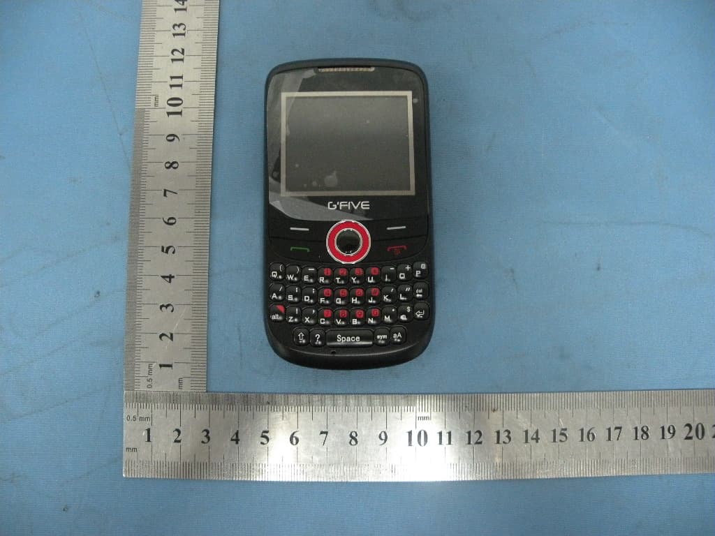
HEO12683
May 15, 2012Mobile Phone
Equipment Class
DSS - Part 15 Spread Spectrum Transmitter