HTG3BPMTS10WTRAVELERS INFORMATION STATION TRANSMITTER
Multi Technical Services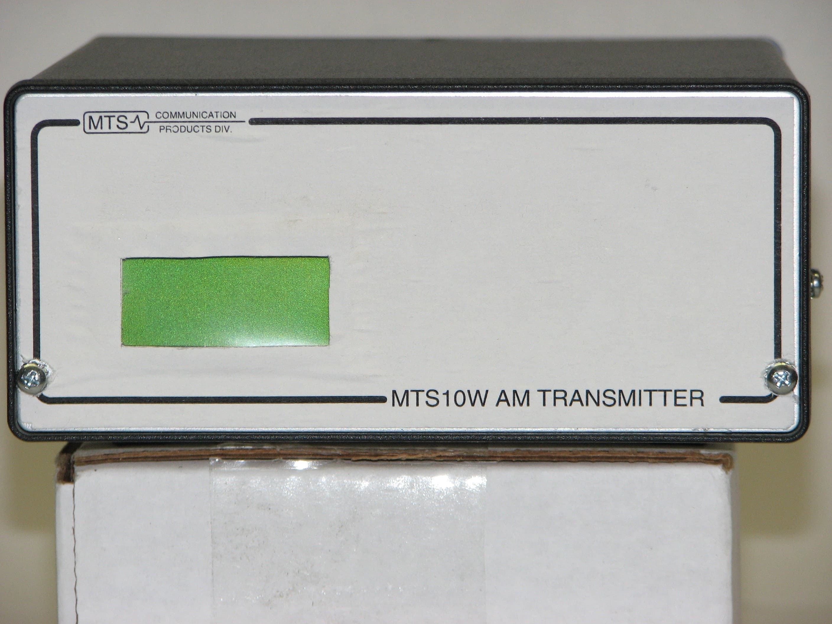
Click to zoom
Application Details
- Equipment Class
- TNB - Licensed Non-Broadcast Station Transmitter
- Date of Grant
- Feb 29, 2012
- Application Purpose
- Original Equipment
- Date of Application
- Feb 29, 2012
- Equipment Note
- TRAVELERS INFORMATION STATION TRANSMITTER
- Frequency Range
- 0.53000000 - 1.70000000
- Company
- Multi Technical Services
- Country
- United States
Documents & Files
Document Text
Text extracted from the exhibit documents filed with the FCC. Open a document above to read the original.
Users Manual
1 February 2012 February 2012February 2012 February 2012 Multi MultiMulti Multi- -- -Technical Services Technical ServicesTechnical Services Technical Services 950 NC Hwy 42 West 950 NC Hwy 42 West950 NC Hwy 42 West 950 NC Hwy 42 West Clayton NC 27520 Clayton NC 27520Clayton NC 27520 Clayton NC 27520 AM Transmitter Travelers’ Information Station Model MTS10W 2 Multi-Technical Services. AM Transmitter Model MTS10W Equipment Manual: MTS10W Transmitter Released: 01/06/2012 Multi-Technical Services. 950 Hwy 42 West Clayton, NC 27520 (919)553-2995 3 Warranty and Limitation of Liability Multi-Technical Services, Inc., hereinafter referred to as MTS, warrants for equipment sold hereunto that for a period of six (6) months from MTS’ shipment date that equipment shall be free from defects in material and workmanship and conform to published specifications for the equipment. If a defect occurs within the warranty period, buyer shall immediately notify MTS and MTS shall repair or replace the defective equipment without extra charge. This warranty does not apply to defects not caused by MTS (for example: lightning damage, accidents or abuse, work or installation done improperly or contrary to MTS standards) or to equipment on which the model or serial numbers, manufacture or shipment dates are changed or removed, or warranty seals broken. No other warranty, expressed, or implied, including but not limited to the implied warranties of merchantability and fitness for a particular purpose, shall apply. Whether or not caused by MTS’ negligence, MTS shall not be liable for any indirect, special, consequential or other damages, however caused (including late delivery). MTS’ obligation to repair or replace equipment in accordance with the above warranty shall be buyer’s exclusive remedy for breach of any warranty or from negligence. If MTS fails to repair or replace as aforesaid, MTS’ entire liability to buyer shall not exceed the repair or replacement value, whichever is lower, of the defective item . 4 Table of Contents Section Description Page One Introduction to the MTS10 5 Two Equipment Specifications 6 Three Installation and Operation 7 Four Software Installation 8 Five Schematic Diagram 9 Six Filter Schematic 10 Seven Component Locator 11 Eight Factory Service Procedure 12 Nine View of the MTS10W 13 Ten View of the MTS10W filter 14 Eleven View of the MTS10W with filter 15 5 Section One Introduction to the MTS10W The MTS10W is an AM Broadcast Band Transmitter designed specifically for application as a transmitter for a Travelers’ Information Station as defined by the Federal Communications Commission Rules and Regulations 47 CFR 90.242. Operation of such a station requires a station license. The MTS10W is a synthesized, solid-state, high efficiency AM transmitter. The design incorporates a high efficiency Class D RF Final amplifier and a Class S high efficiency modulator. The MTS10W is suitable for battery and solar power installations. The power output for the MTS10W is continuously variable from 0.1 watts to 10 watts and does not require any complex power and modulation adjustments. The power adjustment is under software control. The MTS10 is equipped with both a bi-directional power meter and a high performance audio processor with over 30 dB dynamic range to ensure that your transmission is always loud and clear. The MTS10W configuration and control software through the USB interface to your pc allows you to adjust frequency from 530 to 1700 kHz from the drop down menu. Adjustments to RF power output from 0.1 to 10 watts on an easy slide scale, monitor modulation, DC input voltage and forward and reflected power. The MTS10W is covers the US AM broadcast band from 530 to 1700 kHz. The MTS10 is FCC TYPE ACCEPTED, for application in the Travelers’ Information Station service. The FCC Identifier, HTG3BPMTS10W, is located on the rear panel. The MTS10W comes equipped with the following: (1) CD containing software and PDF Manual (2) Power Cable (3) USB cable Make sure all these items are present when unpacking the unit. 6 Section Two Equipment Specifications Physical Height:2.5 inches Length:6.5 inches Width:5.5 inches Weight: 3 pounds Shipping: 5 pounds Environmental Operating: Temperature: -30 to +65 degrees C Humidity: 0 to 95% non-condensing Storage: Temperature: -45 to +80 degrees C Humidity: 0 to 95% non-condensing Input Power: 13.2 Vdc +/- 10% at 2.5 amperes maximum Audio Input monaural 3.5mm Impedance: 600 ohms balanced Level: -30 to +10 dBm 600 ohms, self correcting Transmitter Performance Output Power: 0.1 watts to 10 watts RMS Carrier, continuously variable Output Impedance: 50 ohms Maximum Mismatch VSWR: 3:1 Harmonic and Spurious Emissions: -55 dBc Modulation: A3 Frequency Stability: 100 ppm Hum and Noise: -50 dBc minimum 3 dB Bandwidth: 2.5 kHz, complies with FCC 47CFR 90.242 LCD Display: 2X8 character display 7 Section Three Installation and Operation Safety Notice Installation should be performed by experienced electricians in accordance with national, state and any other electrical codes having jurisdictions. All work should be performed under the direction of the installation or service crew safety foreman. Installation The MTS10W is designed to be installed on a 13.2 Vdc Power supply The power connector, 2 Audio Connectors The audio input connectors are 3.5mm monaural. The audio inputs are 600ohm transformer coupled inputs, so polarity need not be observed. The audio level (-30 to +10 dBm) is not critical and need not be adjusted for changes in carrier power level. Antenna Connector The antenna connector, J3, is the BNC type connector located at the top of the unit. Use 50 ohm coaxial cable, RG-58a/u or equivalent. We recommend that all installations use a coaxial lightning protection device such as the Polyphaser IS- 50UX-CO. The antenna system should be a 50 ohm system and should be installed in such a manner as to comply with FCC Rules (47 CFR 90.242). Not intended for use with leak…
Text truncated - open the document above for the full version.
Block Diagram
D2 K 2 A2 3 A 1 V+ L1 200uH Q1 Q3 IRF520 IRF9520 Q2 U1 24 57 D1 1 J7 21 10K R7 6 CW W CCW D1 D1 2 J5 21 T6 S2S1 P2P1 T5 S2S1 P2P1 J4 12 10k R6 6 CW W CCW 10k R5 2 CW W CCW Q4 IRF520 Q5 IRF520 T4 S3S2 P1 S1 P2P3 10K R8 1 CW W CCW R5 3 CCW W CW 2012- 100 MTS10.S01 01/ 02/ 2012 R.B.E. 11 1 MTS COMMUNICATION PRODUCTS DIVISION9 5 0 NC HIGHWAY 4 2 WESTCLAYTON, NC 27520 (919) 553- 2995 MULTI- TECHNICAL SERVICES, INC. +8 +3.3 +5 3V REGULATOR U1 1 5V REGULATOR U9U1 2 8V REGULATOR CONTRAST ADJ J8 LCD MODULE PROGRAMMING PORT PROCESSOR FIRMWARE J1 USB CONFIG PORT J2 20 MHZ X1 MICRO CONTROLLER U2 X2 10 MHZ TCXO U5 OSCILLATOR NUMERICALLY CONTROLLED OUTPUT /Q Q IN RF FINALRF FINAL RF TRANSFORMER FET DRIVER U3 RF FILTER MODULE P1:2 P1:1 PEAK RECTIFIER D1 0 U8 :B ALT AUDIO IN AU DIO SWITCH U4 PRI AUDIO IN 3.4 KHZ AUDIO FILTER U7 VR TRIM VF TRIM U6 BUFFER VR VF OUTPUT J3 T1 , T2 , T3 , D6 AN D D7 B I- DIRECTION AL WATT METER AUDIO COMPANDOR MODULATION SET LEVEL SHIFTER MODULATION AMPLIFIER U8 A U1 0 AU DIO FILTER FREQUENCY TRIM MODULATION FILTER PWM DRIVER POWER CONTROL MODULATION CONTROL MODULATOR Block Diagram MTS10W Transm itter ABCDEF GH 654321 H G F E D C B A 12 3 456 D Rev Num ber Ti t l e Size Da t eFilenam e Dr a wn b y of Sheet
External Photos
Front View MTS10W Transmitter Side View MTS10W Transmitter Rear Panel View MTS10W Transmitter
ID Label/Location Info
MADE IN THE USA MODEL MTS10W MTS COMMUNICATION PRODUCTS CLAYTON, NC USA 12VDC 3A FCC ID: HTG3BPMTS10W PGM ALTERNATE PRIMARY AUDIO AUDIO USB POWER OUTPUT TRAVELERS INFORMATION SERVICE TRANSMITTER PRODUCTS DIV. COMMUNICATION MTS
Internal Photos
MTS10W Main PCB Assembly, Top View MTS10W Main PCB Assembly Bottom View MTS10W Filter Assembly Top View MTS10W Filter Assembly Bottom View MTS10W Inside View Top Front MTS10W Inside View Side MTS10W Inside View Rear
Operational Description
Theory of Operation: MTS10 10 Watt AM Transmitter Referenced Documents: Attachment 1 Block Diagram Attachment 2 Schematic Diagram Attachment 3 Filter Schematic Diagram Section 1.0 General Description General The MTS10 Transmitter is a 10 watt AM Broadcast band transmitter designed to comply with FCC Rules Part 97.242 Travelers Information Station Requirements. The unit is synthesized and covers from 530 kHz to 1700 kHz in 10 kHz steps. The transmitter frequency is set by running a configuration utility on a personal computer connected to the unit. This USB connection is a one time connection for configuration purposes only and is not designed nor intended to remain connected at any time after the initial configuration. The power level which is continuously adjustable from 0.1 to 10.0 watts is also set using the USB configuration utility. Additional features in the USB configuration utility include a visual indication of modulation, a display of the transmitters forward and reflected power to the antenna system, selection of which audio input is active, selection of which mode the audio selection is in, and a display of the DC input voltage to the unit. The MTS10 employs a Class D RF amplifier and a Class S modulator which yields outstanding power efficiency and reduced operation costs. The efficiency is for a fully modulated output is 82% minimum and can be as high as 92% depending on frequency and the antenna characteristics. Input Power Input Power to the MTS10 is nominally 13.2 Volts DC at a maximum current of 2.5 amperes. The connection for the DC input power is at J7. MTS recommends that you use only the provided power cable with the unit as the current rating for this connector is for a specific model of the coaxial power connector. Audio Input. The MTS10 has two audio inputs, Primary and Alternate, at J4 and J5 respectively. J4 and J5 are monaural 3.5mm jacks and the inputs are both 600 ohm transformer coupled. The nominal audio input level is -10 dBm for full Page 1 of 5 modulation, however this level is not critical. The MTS10 has a compandor circuit that automatically adjusts the gain of the modulator to accommodate input levels from -30 dBm to +10 dBm. It is not possible to over modulate the transmitter regardless of the audio input level. This is due to the modulator employing a pulse width modulation that is generated by the microprocessor and having a maximum pulse duration of 99%. RF Output The RF output is at J3 on the rear panel which is a BNC type connector. The RF output is a 50 ohm output and should only be connected to 50 ohm antennae or 50 ohm loads. The transmitter is protected from large mismatches to the load. It will not damage the unit if the output is opened or shorted, repetitively. There are certain load conditions that may cause the unit to operate at higher than normal or desirable temperatures, but these conditions should not exist in normal serviceable installations. LCD Display The MTS10 has a front panel LCD display that displays various information about the condition of the unit. It displays the unit serial number on power up, frequency, forward and reflected power, and a visual indication of modulation. RF Filters The MTS10W has three 5 th order elliptical filters that are selected by the processor for RF Filtering. The filters are for 530-750 kHz, 760 kHz to 1100 kHz and 1110 kHz to 1700 kHz. The filters are located on the plug in Filter Assembly at P1. Audio Filter The MTS10 is equipped with the 3.4 kHz Modulation Filter as required by FCC Part 90.242. Section 2.0 Micro Controller Circuitry U2 is the embedded Micro Controller that controls the transmitter. U2 is operated from the regulated 5V supply. U2 has a 20 MHz crystal oscillator, X1, that provides its clock signal. U2 provides: a. Programming data for the numerically controlled oscillator, U5 b.Data for the LCD Display c.Control data for the Audio input selector switch, U4. Page 2 of 5 d.USB interface for user programming of the radio and firmware updates. e.A pulse width modulated signal for the Power Control circuitry. This PWM is at 186 kHz and can be varied from 1% to 99% f.A pulse width modulated signal for the Modulator circuitry. This PWM signal is at 186 kHz and can be varied from 1% to 99%. g.Analog to Digital conversion for the Forward Power and Reflected Power signals from the bidirectional wattmeter circuitry. h.Drive for LED D12 that is the ‘operating’ indicator for the processor. i.Filter detection for determining what RF filter module is installed. Section 3.0 Numerically Controlled Oscillator The operating frequency of the transmitter is determined by programming U2 with the appropriate control and data words to divide its reference oscillator, 10 MHz temperature compensated crystal oscillator X2, to the correct frequency. The maximum error is less than 10 Hz, from either division error or temperature drift or the combination of both. X2 and U2 are powered by the 3.3 volt regulated DC supply, U11. Provisions for operating the synthesizer from an external reference source have been made at J6. Section 3.1 RF Section The output of the numerically controlled oscillator directly drives U3 a differential FET driver IC. This IC provides highly duty cycle accurate, current limited drive to the RF Final MOSFETs, Q4 and Q5. Q4 and Q5 are operated in the CLASS D Mode. RF Transformer T4 converts the low impedance of the amplifier (2.7 ohms) to nearly 50 ohms. The center tapped primary of the RF Transformer is output of the modulation filter. Note that the DC from the power control flows through the filter and provide the current which is switched to create the RF carrier in the primary. The modulator varies the DC to create high level AM. Section 3.2 RF Filters The RF Filter Module mount just above the main board at P1. The filter design is a 5 th order Cauer design which provides excellent in band loss characteristics as well as excellent attenuation to out of band signals. An approxim…
Text truncated - open the document above for the full version.
Parts List/Tune Up Info
MTS10W Transmitter Manufacturing Test Procedure Assemble test equipment per equipment list and Fig 1. (1) Set the audio oscillator output to 0. (2) Connect the Unit Under Test as shown in Figure 1. (3) Apply power. (4) Adjust Pot R76, LCD Contrast Adjustment, for correct contrast. (5) Start the MTS10W configuration software on the computer. (6) Set the operating frequency to 530 kHz by using the drop down frequency control. (7) Using the power control slider, adjust the power for 22.4 Volts on the RF Voltmeter. (8) Set Pot R66 for an indication of 10.0 watts Forward Power on the LCD Display. (9) Disconnect the RF Load at the transmitter. (10) Set Pot R59 such that the Forward and Reflected power indicated at the LCD are the same. (11) Reconnect the RF Load and note that the Reflected power indicated in the LCD is less than 0.2 watts. (12) Check the indicated RF Voltage across the load and note that it is within 0.2 Volts of 22.4 Volts RMS. This insures that the transmitter power is within 0.2 dB of its rated 10 watt output (+40 dBm 50 ohms). (13) Note that the frequency counter indicates 530 KHz +/- 2 Hz. (14) Change the frequency to 750, 990, 1000, 1010, 1350, and 1700 kHz. After each frequency change perform steps 15 and 16 below. (15) Note the output voltage is 22.4 Volts, the RF power disp[layed on the LCD is 10 watts. (16) Note the frequency counter indicates the selected frequency +/- 2 Hz. (17) Set the Audio Oscillator frequency to 3.2 kHz. Set the amplitude to 0 dBm. Connect the oscilloscope probe to U7 pin 5. Adjust R53 such that the amplitude of the signal decreases with any increase in frequency. There should be no apparent change in amplitude below 3.2 kHz but the amplitude should decrease noticably by 3.3 kHz. (18) Set the Audio Oscillator frequency to 1 kHz. Set the amplitude to -20 dBm. Adjust the Modulation Control, R81, for 98% Modulation as indicated on the Oscilloscope. (19) Adjust the Audio Oscillator amplitude to +10 dBm and note the Oscilloscope display continues to indicate 98% Modulation. (20) Install the Transmitter assembly in its cabinet and burn-in at 50 degrees C for 48 hours and repeat steps 1 thru 19. MasTech MS6100 Frequency Counter HP4734A HP 204C Step Attenuator 02/17/2012 By: L. Williams Page: : Test Setup Manufacturing Test Setup MULTI-TECHNICAL SERVICES, INC. RF OUT DC IN 13.2 VDC SUPPLY UUT Audio Oscillator 50 OHM LOAD Oscilloscope HP 6263B TEK 2225 BIRD TENULINE MODEL 8329
Parts List/Tune Up Info
MTS10W PARTS LIST Resistors 1 1.1K MCR10EZPJ112 R69 5 10 MCR10EZPJ100 R2,43,49,54,84 6 100 MCR10EZPJ101 R31,35,38,40,41,42 9 100K MCR10EZPF1003 R14,34,37,44,47,50, 51,26,27 25 10K MCR10EZPF1002 R1,6,7,11,16,19,23, 29,32,45,55,61,63, 67,70,77,83,85,87, 91,48,65,72,79,82 9 1K MCR10EZPJ102 R30,33,39,60,62,68, 86,46,64 1 2.26K RC0805FR-072K26L R74 1 2.2K RC0805JR-072K2L R58 1 2.49k RC0805FR-072K49L R75 2 220 1/2 ERJ-14YJ221U R18,21 1 20K RC0805FR-0720KL R59 3 27 RC0805JR-0727RL R3,5,9 2 3K RC0603JR-073KL R56,57 3 4.7 RC0805JR-074R7L R10,17,22 5 4.7K RC0805JR-074K7L R13,15,20,28,36 3 4.99K RC0805FR-074K99L R73,R78,R80 1 470 RC0805FR-07470RL R90 1 49.9K RC0805FR-0749K9L R8 2 5.6K RC0805FR-075K6L R4,12 2 51 RC0805FR-0751RL R24,25 1 68K RC0805JR-0768KL R71 Pots 5 10K D1AA14 R53,76,81,52,66 Capacitors 5 0.01 GRM216R71H03KA01D C33,42,59,68,72,24,25 2 0.022 GRM216R71H223KA01D C69,71,35 12 0.1 ERJ-14YJ221U C17,20,21,27,28,31,46,56,57,62,64,48,58,60,67,73,74 3 0.47 CC0805KKX7R8BB474 C7,15,65 1 100uF UWX1C101MCL1GB C4 1 2.2uF C2012X5R1A225M/0.85 C61 2 20pF 08051A200JAT2A C5,8,32 16 22uF JMK212BJ226MG-T C6,16,22,26,30,34,36,37,43,44,45,47,52,54,55,66 1 2200pF GRM32A7U2J222JW31D C70 1 470pF CC0805KRX7R9BB471 C29 1 1uF C2012Y5V1C105Z/0.85 C2 6 10uF EMK212BJ106KG-T C1,18,38,41,53,63 2 10,000uF ECO-S1CA103CA C3,49 3 15uF B32524Q1156K C11,12,14 3 1uF ECQ-E2105KB C9,10,13 Diodes 1 SP0503BAHTG D1 2 1N34A D6,D7 2 1N4148-WS D3,D5,D10 1 RS2A-13 D11 1 LH R974-LP-1 D12 1 MBR1545CT D2 Transistors 3 IRF520 Q3,4,5 2 IRF9520 Q1,2 Integrated Circuits 1 THAT4320 U10 1 EL7222 U3 1 L78M05 U9 2 LM358N U6,8 1 LM78L08ACM U12 1 TLC04 U7 1 LP2985-3.3 U11 1 MK1716 U5 1 CD4066B U4 1 PIC18F4550 U2 1 ICL7667 U1 Crystals and TCXOs 1 20.000 MHz HCM49 X1 1 FOX924-10MHz X2 Inductors 1 200uH MTS10-1001 L1 1 222uH MTS10-1002 L3 1 248uH MTS10-1003 L2 1 495uH MTS10-1004 L4 Transformers 3 MTS10-1005 T1,T2,T3 2 Midcom 671-8013 T5,T6 1 MTS10-1006 T4 Switches 1 101-0363-EV S1 Connectors 1 BNC 571-5415085-1 J3 1 2.1x5.5 AD-0202-2.1 J7 1 Header 5 pin SIL 517-9611056404AR J1 1 3.5mm Stereo jack AJE3531-3 J4,J5 1 4 pos header SIL 517-9611046804AR J6 1 8 pos header SIL P1 1 USB Jack Type B CU02SAH0000 J2 Misc 1 MTS 7200-100 Printed Circuit Board 1 MTS 7200-125 Enclosure 1 MTS 7200-126 Front Panel 1 MTS 7200-127 Rear Panel 1 MTS 7200-131 Front Panel Overlay 1 MTS 7200-132 Rear Panel Overlay 1 MTS 7200-128 Heat Sink 6 TO220 Mounting Kits 3 #4-40x0.75 Round Standoff 16 #4-40x0.25 PHMS 4 #4-40x0.50 PHMS LCD Assembly 2 MTS 5700-102 Printed Circuit 1 LCD Assembly 2F08DNLY-E 2 Header, 2 x 7 DIL Connector 1 Header 1 x 7 SIL Connector 2 Header 1 x 1 SIL Connector Pin RF Filter Assembly 2 Relay DS2Y-12 K1,K2 1 CAP0805 0.22uF C4 2 CAP1210 100pF C3,C10 4 CAP1210 1100pF C9,C18,C23,C24 1 CAP1201 1200pF C26 2 CAP1210 1500pF C11,C21 2 CAP1210 1800pF C36,C37 3 CAP1210 2000pF C8,C17,C31 1 CAP1210 2200pF C30 2 CAP1210 200pF C2,C38 2 CAP1210 220pF C28,C32 2 CAP1210 20pF C12,C29 1 CAP1210 39pF C27 2 CAP1210 300pF C14,C16 1 CAP1210 3300pF C20 3 CAP1210 330pF C13,C15,C22 2 CAP1210 470pF C1,C25 2 CAP1210 620pF C5,C6 1 CAP1210 6800pF C34 1 CAP1210 680pF C7 1 CAP1210 68pF C19 4 DIODE 4148 D1,D2,D3,D4 1 IDC1X8F P1 1 INDI 10.3uH/33T L6 1 INDI 12.5/36 L5 1 INDI 4.7uH/23T L2 1 INDI 5.7uH/25T L1 1 INDI 6.9uH/26T L4 1 INDI 8.3uH/30T L3 2 NPN M3904 Q1,Q2 2 RES0805 10K R2,R4 2 RES0805 1K R1,R3 1 7001-201 Printed Circuit Board (END)
Schematics
C2 3 0.22 100K R5 1 VSS VSS VSS VCC VSS VSS V+ 0.22 C7 4 0.22 C7 3 LM78L08ACM U1 2 GND 7 GND 2 GND 6 GND 3 VOU T 1 VIN 8 10K R8 7 VCC 10 R8 4 VDD VCC VCC VCC VCC VDD VDD VDD VCC V+ V+ 0.22 C1 9 10uF C1 8 4.7 R1 0 EL7222 U3 63 75 42 0.22 C6 0 10K R8 1 CW W CCW 10K R8 3 22uF C6 6 10K R8 5 R7 710K 10K 1% R7 9 10uF C6 3 R8 2 10k 1% U8 :A LM1458N 1 84 + 3 - 2 C5 8 0.22 R7 1 68K 4148 D1 0 1K R6 2 10K R6 3 100K R5 0 100K R4 7 LM1458N U8 :B - 6 + 5 7 10uF C3 8 22uF C4 4 10K R6 7 1K R6 0 T6 S2S1 P2P1 2.2K R5 8 C3 9 0.22 22uF C2 2 100K R4 4 100K R3 7 100K R3 4 22uF C2 6 1K R3 9 1K R3 3 U4 :A CD4066BF O/ I 2 I/ O 1 CONT 13 CD4066BF U4 :C CONT 6 I/ O 8 O/ I 9 CD4066BF U4 :D CONT 12 I/ O 11 O/ I 10 CD4066BF U4 :B CONT 5 I/ O 4 O/ I 3 VCC 1K R3 0 T5 S2S1 P2P1 R7 0 10K C4 0 0.22 VCC R5 5 10K VCC C2 8 0.1 U7 TL C0 4 CL 1 CR 2 GN D 4 OUT 5 FILIN 8 +12 7 VAG 6 GN D 3 1.1K R6 9 0.01 C4 2 C4 1 10uF 10K R6 1 10k R7 2 4.99k R7 3 22pF C3 2 20K R5 9 3K R5 6 3K R5 7 0.01 C3 3 .022 C3 5 4.99k R8 0 2.26K R7 4 0.01 C5 9 0.47 C6 5 22uF C4 7 0.1 C6 2 2.49k R7 5 10uF C5 3 0.1 C5 7 0.1 C4 6 22uF C5 2 THAT4320 U1 0 VEE 28 GN D 1 OUT3 20 IN3- 21 VCAIN 23 VREF 11 VPTAT 9 RMSOUT 8 CT 7 RMSIN 6 IN4+ 18 IN4- 17 OUT4 16 BUFFER 13 VCC 15 GN D 14 OUT1 25 OUT2 4 IN2- 3 IN2+ 2 IN1- 26 IN1+ 27 3 IN VCA OUT EC- EC+ RMS 4 VCC 2 1 VCC 4.99k R7 8 0.1 C5 6 R4 3 10 R4 9 10 R5 4 10 C3 4 22uF C3 6 22uF C3 7 22uF MK1716 U5 VDD 22 VDD 23 VDD 24 OE 25 SRCLK 26 STROBE 27 GN D 21 GN D 20 CLKB 19 CLKB 18 CLKB 17 CLKB 16 VDDIOA 14 VDDIOB 15 GN D 28 CLKA 13 CLKA 12 CLKA 11 CLKA 10 GN D 7 GN D 8 GN D 9 VDD 6 VDD 5 ROUT 4 X1 3 X2 2 DATA 1 R4 0 100 R4 1 100 R4 2 100 R3 1 100 R3 5 100 R3 8 100 X2 FOX924 NC 1 GN D 2 OUT 3 VCC 4 0.1 C3 1 R4 5 10K R3 2 10K R2 3 10K 10K R1 9 R1 5 4.7k R2 0 4.7k R2 8 4.7k R3 6 4.7k 200 1/ 2W R2 1 200 1/ 2W R1 8 Q4 IRF520 Q5 IRF520 T4 14CT20 S3S2 P1 S1 P2P3 R1 7 4.7 R2 2 4.7 R2 9 10K R1 6 10K P1:1 1 2 3 4 5 6 7 8 T1 S2 S1 P2 P1 C2 4 .01 C2 5 .01 D7 1N34A D6 1N34A R2 7 100k R2 6 100k T2 S2S1 P2P1 R2 4 51 T3 S2S1 P2P1 R2 5 51 J3 12 VCC C1 1 15uF C1 2 15uF 1uF C1 3 L3 222uH 15uF C1 4 495uH L4 10 R2 5.6K R4 27 R5 1N4148 D3 27 R3 0.47 C7 100 C4 10K R6 10K R7 ICL7667U1 63 75 42 Q2 IRF9520 IRF520 Q3 27 R9 5.6K R1 2 1N4148 D5 0.47 C1 5 248uH L2 C1 0 1uF C9 1uF 0.1 C6 4 LP2985 U1 1 BYP 4 ON 3 VIN 1 VOU T 5 GND 2 C6 1 2.2uF C5 4 22uF 22uF C5 5 10K R7 6 CW W CCW VCC J7 21 RS2A13 D1 1 C4 8 0.1uF C4 9 10,000uF V+ U9 L78M05 VO 3 G 2 VI 1 C5 0 0.22 C5 1 0.22 VCC J6 4321 R1 10K J1 54321 0.1 C1 7 10K R1 1 49.9K R8 1uF C2 22uF C6 22uF C1 6 SP0503BAHTGD1 1 4 3 2 J2 4321 PIC18F4550 U2 C0 32 OSC2 31 OSC1 30 VSS 29 VDD 28 E2 27 E1 26 E0 25 A5 24 C2 36 VUSB 37 D0 38 D1 39 D2 40 D3 41 C4 42 C5 43 C1 35 ICPORTS 34 C6 44 ICRST 33 A4 23 A3 22 A2 21 A1 20 A0 19 /MCLR 18 B7 17 B6 16 B5 15 B4 14 ICPGD 13 ICPGC 12 B3 11 B2 10 B1 9 B0 8 VDD 7 VSS 6 D7 5 D6 4 D5 3 D4 2 C7 1 X1 20 C5 20pF C8 20pF R1 3 4.7K R1 4 100K S1 C1 C2 R5 3 10K CCW W CW C2 9 470pF J8 1413121110987654321 J9 7654321 10k R6 6 CW W CCW 10k R5 2 CW W CCW 22uF C3 0 1k R4 6 U6 :A LM358N 1 84 + 3 - 2 C2 7 0.1 R4 8 10k R6 5 10k U6 :B LM358N 7 + 5 - 6 R6 4 1k C4 3 22uF D1 2 D1 2 R9 0 470 R9 1 10K C6 7 0.22 VCC C7 1 0.022 0.1 C2 0 0.1 C2 1 C7 0 2500pF C6 9 0.022 J5 12 C7 2 0.01 J4 12 C6 8 0.01 10uF C1 Q1 IRF9520 200uH L1 V+ C3 10,000uF D2 MBR1545 A 1 A2 3 K 2 R6 8 1K C4 5 22uF R8 6 1K ANTENNA MULTI- TECHNICAL SERVICES, INC. (919) 553- 2995 CLAYTON, NC 275209 5 0 NC HIGHWAY 4 2 WESTMTS COMMUNICATION PRODUCTS DIVISION 11 1 R.B.E. 01/ 02/ 2012 MTS10.S01 2012- 100 TX 1 0 TIS Tr a n s m i t t e r ES GROUND 5V CONTRAST R/ W ENABLE DB0DB1DB2DB3DB4DB5DB6DB7 1 0 MHZ TCXO FILTER MODULE PRI AUDIO IN ALT AUDIO IN + 13.2 VDC IN B2 A0 D2 D3 D0D1 C1 C2 B0 B6B7 MCLR E0 A5 C6 B1 A0 A1 A2 A3 MCLR B5 B4 A4A5E1E2C0RST ICP C1 C2 D0 D1 D2 D3 C7D4D5D6D7B0B3 B7 B6 B7B6B5B4 B3B2 B7 B6 A2 A3 C0 MCLR A1 ABCDEF GH 654321 H G F E D C B A 12 3 456 D Rev Num ber Ti t l e Size Da t eFilenam e Dr a wn b y of Sheet 0.22 C4 1KR31KR1 10K R4 10K R2 4148 D4 4148 D2 M3904 Q2 M3904 Q1 4148 D3 4148 D1 K2 16 1 91186 4 13 K1 16 1 91186 4 13 P1:1 12345678 1500pF C1 1 620pF C5 620pF C6 100pF C1 0 2000pF C8 680pF C7 4.7uH/ 24T L2 5.7uH/ 26T L1 20pF C1 2 1200pF C2 4 1500pF C2 2 1500pF C2 1 2000pF C1 7 620pF C1 8 1200pF C2 3 1500pF C2 0 180pF C1 9 6.9uH/ 26T L4 8.3uH/ 30T L3 200pF C1 6 300pF C1 4 330pF C1 3 C2 6 1200pF C2 7 39pF L5 12.5uH/ 36T L6 10.3uH/ 33T C3 6 1800pF C3 1 2000pF C3 0 2200pF C3 4 6800pF C3 7 1800pF 200pF C2 300pF C1 5 C2 8 220pF 1100pF C9 C1 470pF C3 100pF C3 2 220pF 0 01- 27- 2012 7001- 201 760 to 1000 1010 to 1700 530 to 750 RF IN RF OUT GN DGN D R1R2 +12 RF OUT (919) 553- 2995 CLAYTON, NC 27520 9 5 0 NC HIGHWAY 4 2 WEST MTS COMMUNICATION PRODUCTS MTS10FLT.S01 LAW 1 1 MTS- 1 0 AM FILTER A BC D 4 321 D C B A 1 2 3 4 B Rev Num ber Ti t l eSizeDa t eFilenam e Dr a wn b y of Sheet
Test Report
FCC Report of Measurements FCC ID HTG3BPMTS10W MTS10W 10 Watt AM Transmitter Part 90.242 Travelers Information Station Multi-Technical Services, Inc. 950 NC Highway 42 West Clayton, NC 27520 February 21, 2012 Compiled by: Lynwood A. Williams Telephone: (919) 553-2995 Email: [email protected] TABLE OF CONTENTS Report of Measurements 47 CFR 2.1046 RF power output Rule Citation 4 Data 5 Test setup drawing 6 Schematic 7 Photograph of equipment 8 47 CFR 2.1047 Modulation characteristics Rule Citation 9 Data 10 Test setup drawing – modulation filter response 11 Schematic 12 Data 13 Test setup drawing – modulation characteristics 14 Photograph of equipment 15 47 CFR 2.1049 Occupied bandwidth Rule Citation 16 Data 17 Test setup drawing 18 Photograph of measurement 19 47 CFR 2.1051 Spurious emissions at antenna terminals Rule Citation 20 Data 21 Test setup drawing 23 Photograph of equipment 24 47 CFR 2.1055 Frequency stability Rule Citation 25 Data 27 Test setup drawing 30 Photographs 31 47 CFR 2.1057 Frequency spectrum investigated Rule Citation 34 Data 35 Test setup drawing 44 Photographs 45 47 CFR 90.242 Modulation Filter Response Rule Citation 46 Data 47 Test setup drawing 48 Schematic 49 Measurement Facilities Report 50 Measurement Equipment 51 Measurement Facility Statement 53 Drawing 54 Photographs 55 47 CFR 90.242 (B) (3) Concerning leaky cable statement 57 Modification Report 1. Cover: modified to show new date 2. Table of contents: modified page numbers and added additional menu items 3. 47 CFR 2.1051 Spurious emissions at antenna terminals : changed photographs to show new data (pages 21 and 22) 4. 47 CFR 2.1057 Frequency spectrum investigated : changed data and photographs to show data for new filters ( pages 35 to 43 ) 5. 47 CFR 90.242 (B) (3) concerning leaky cable applications: section added (page 57) 6. Measurement Equipment: Calibration column added (page 51-52) 2.1046—RF power output. (a) For transmitters other than single sideband, independent sideband and controlled carrier radiotelephone, power output shall be measured at the RF output terminals when the transmitter is adjusted in accordance with the tune-up procedure to give the values of current and voltage on the circuit elements specified in § 2.1033(c)(8). The electrical characteristics of the radio frequency load attached to the output terminals when this test is made shall be stated. (b) For single sideband, independent sideband, and single channel, controlled carrier radiotelephone transmitters the procedure specified in paragraph (a) of this section shall be employed and, in addition, the transmitter shall be modulated during the test as follows. In all tests, the input level of the modulating signal shall be such as to develop rated peak envelope power or carrier power, as appropriate, for the transmitter. (6) Single-channel controlled-carrier transmitters in the A3 emission mode--by a 2500 Hz tone. (c) For measurements conducted pursuant to paragraphs (a) and (b) of this section, all calculations and methods used by the applicant for determining carrier power or peak envelope power, as appropriate, on the basis of measured power in the radio frequency load attached to the transmitter output terminals shall be shown. Under the test conditions specified, no components of the emission spectrum shall exceed the limits specified in the applicable rule parts as necessary for meeting occupied bandwidth or emission limitations. 4 Carrier Frequency: 530 KHz Volts DC from point B to ground5.09VDC Current measured at point A to B2.69A RF Output Volts22.65V RF Output Power10.26W Carrier Frequenc y: 1120 KHz Volts DC from point B to ground4.99VDC Current measured at point A to B2.73A RF Output Volts22.7V RF Output Power10.3W Carrier Frequenc y: 1690 KHz Volts DC from point B to ground5.43VDC Current measured at point A to B2.41A RF Output Volts22.1V RF Output Power9.77W Carrier Frequenc y: 530 KHz with 2500 Hz tone Volts DC from point B to ground4.75VDC Current measured at point A to B2.4A RF Output Volts33.6V RF Output Power31.93W PEP Carrier Frequenc y: 1120 KHz with 2500 Hz tone Volts DC from point B to ground4.65VDC Current measured at point A to B2.45A RF Output Volts34.1V RF Output Power32.88W PEP Carrier Frequenc y: 1690 KHz with 2500 Hz tone Volts DC from point B to ground4.96VDC Current measured at point A to B2.14A RF Output Volts33.4V RF Output Power POWER CALCULATIONS P = E^ 2 / R for carrier carrier x 1.414 for PEP 31.55W PEP 5 Generator Audio HP204C 2.23 0.1 1/15/2012 By: L. Williams Page: : Test Setup DC Input Power Measurement Multi-Technical Services, Inc. 22.3619.3615.8110.07.075.0 2.01.00.5 Rf Volts Watts RF Power Table are shown on next pagePoints A, B To GroundTo "B"To "B"To "A" Fluke 77 DC Current Fluke 77 DC Volts RF OUT DC IN 100:1 13.2 VDC Supply RF Volt Meter UUT 50 Ohm Load 5.07.5 10.0 HP6263B Bird Tenuline Boonton 92BD with 100:1 probe Model 8329 6 C2 3 0.22 100K R5 1 VSS VSS VSS VCC VSS VSS V+ 0.22 C7 4 0.22 C7 3 LM78L08ACM U1 2 GND 7 GND 2 GND 6 GND 3 VOU T 1 VIN 8 10K R8 7 VCC 10 R8 4 VDD VCC VCC VCC VCC VDD VDD VDD VCC V+ V+ 0.22 C1 9 10uF C1 8 4.7 R1 0 EL7222 U3 63 75 42 0.22 C6 0 10K R8 1 CW W CCW 10K R8 3 22uF C6 6 10K R8 5 R7 710K 10K 1% R7 9 10uF C6 3 R8 2 10k 1% U8 :A LM1458N 1 84 + 3 - 2 C5 8 0.22 R7 1 68K 4148 D1 0 1K R6 2 10K R6 3 100K R5 0 100K R4 7 LM1458N U8 :B - 6 + 5 7 10uF C3 8 22uF C4 4 10K R6 7 1K R6 0 T6 S2S1 P2P1 2.2K R5 8 C3 9 0.22 22uF C2 2 100K R4 4 100K R3 7 100K R3 4 22uF C2 6 1K R3 9 1K R3 3 U4 :A CD4066BF O/ I 2 I/ O 1 CO…
Text truncated - open the document above for the full version.
Contact Information
Applicant
Lynwood A Williams
Technical Specifications
| # | Rule Parts | Frequency Range | Power Output | Emission | Tolerance |
|---|---|---|---|---|---|
| 1 | 90 | 0.53 MHz - 1.7 MHz | 10 W | 6K00A3E | 100.0000000000 Hz |
Other Applications from Multi Technical Services
HTG3000D
Nov 17, 1996CXX - Communications Rcvr for use w/ licensed Tx and CBs
Equipment Class
CXX - Communications Rcvr for use w/ licensed Tx and CBsHTG3BP1085A
Jun 12, 1989EBD - Unkown (From ALTOS)
Equipment Class
EBD - Unkown (From ALTOS)