J4CTRM303Fleetwatch TRM303
S&A Systems Inc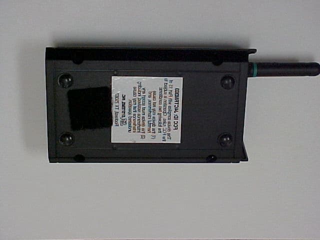
Click to zoom
Application Details
- Equipment Class
- DXT - Part 15 Low Power Transceiver, Rx Verified
- Date of Grant
- Dec 19, 2001
- Application Purpose
- Original Equipment
- Date of Application
- Dec 19, 2001
- Equipment Note
- Fleetwatch TRM303
- Frequency Range
- 303.87500000 - 303.87500000
- Company
- S&A Systems Inc
- Country
- United States
Documents & Files
Document Text
Text extracted from the exhibit documents filed with the FCC. Open a document above to read the original.
Users Manual
i MOBILE RECEIVER HARDWARE MANUAL TRM303 ii Copyright © 2001, S&A SYSTEMS, INC. All Rights Reserved. No part of this document may be copied or reproduced in any form or by any means without the prior written consent of S&A SYSTEMS, INC. S&A SYSTEMS, INC. makes no warranties with respect to this documentation and disclaims any implied warranties of merchantability and fitness for a particular purpose. Information in this document is subject to change without notice. S&A SYSTEMS, INC. assumes no responsibility for any errors that may appear in this document. From time to time changes may occur on the file names and in the files actually included on the distribution disks. S&A SYSTEMS, INC. makes no warranties that such files or facilities, as mentioned in this documentation, exist on the distribution disks or as part of the materials distributed. FLEETWATCH and S&A SYSTEMS, INC. are registered trademarks of S&A SYSTEMS, INC. IBM is a registered trademark of International Business Machines Corporation. Copyright iii FCC Statement This equipment has been tested and found to comply with the limits for a Class B digital device, pursuant to Part 15 of the FCC Rules. These limits are designed to provide reasonable protection against harmful interference in a residential installation. This equipment generates, uses and can radiate radio frequency energy and, if not installed and used in accordance with the instructions, may cause harmful interference to radio communi- cations. However, there is no guarantee that interference will not occur in a particular installation. If this equipment does cause harmful interference to radio or television reception, which can be determined by turning the equipment off and on, the user is encouraged to try to correct the interfer- ence by one of the following measures: ◆Reorient or relocate the receiving antenna. ◆Increase the separation between the equipment and receiver. ◆Connect the equipment into an outlet on a circuit different from that to which the receiver is connected. ◆Consult the dealer or an experienced radio/TV technician for help. Changes or modifications not expressly approved for compliance by S & A SYSTEMS, INC. could void the user’s authority to operate the equipment. It is necessary to use shielded interconnect cables to insure compliance with FCC Class B limits for radio frequency emissions. FCC Statement 1v S&A SYSTEMS, INC. SOFTWARE LICENSE AGREEMENT This document is a legal agreement between you, the licensee, and S&A SYSTEMS, INC. By using this program, you are agreeing to become bound by the terms of this agreement. If you do not agree to the terms of this agreement, promptly return the disk package and the other items that are part of this product, in their original package, with your payment receipt, to S&A Systems for a full refund. In Consideration of payment of the License Fee, which is part of the price evidenced by the receipt, S&A SYSTEMS, INC. grants to the Licensee a nonexclusive right, without right to sublicense, to use this copy of this S&A SYSTEMS, INC. Software on a single Computer at a time. S&A SYSTEMS, INC. reserves all rights not expressly granted, and retains title and ownership of Software, including all subsequent copies in any media. This software and the accompanying written materials are copyrighted. You may copy the Software solely for backup purposes; all other copying of the Software of the written materials is expressly forbidden. As the only warranty under this Agreement, and in the absence of accident, abuse, or misapplication, S&A SYSTEMS, INC. warrants, to the original Licensee only, that the disk(s) on which the Software is recorded is (are) free from defects on materials and workmanship under normal use and service for a period of ninety (90) days from the date of payment as evidenced by a copy of the receipt. S&A SYSTEMS, INC.’s only obligation under this Agreement is, at S&A SYSTEMS, INC.’s option, to either (a) return payment as evidenced by a copy of the receipt, or (b) replace the disk that does not meet S&A SYSTEMS, INC.’s limited warranty and which is returned to S&A SYSTEMS, INC. with a copy of the receipt. This warranty gives you limited, specific legal rights. You may have other rights, which vary from state to state. The Software and accompanying written materials are provided “as is”, without warranty of any kind, including the implied warranties of merchantability and fitness for a particular purpose, even if S&A SYSTEMS, INC. has been advised of that purpose. S&A SYSTEMS, INC. specifically does not warrant the operation of the Software and will not be liable for any direct, indirect, consequential, or incidental damages arising out of the use of or inability to use such product, even if S&A SYSTEMS, INC. has been advised of the possibility of such damages. Some states do not allow the exclusion or limitation of liability for consequential or incidental damages, so the above limitations may not apply to you. Software License Agreement v Table Of Contents Section 1 Introduction.......................................................................................1 Program Requirements.......................................................................1 Contacting Technical Support .............................................................1 Section 2 Installation.........................................................................................3 Connecting the TRM303 Hardware .....................................................3 Installing the TRM303 Interface Software...........................................5 Section 3 Using the TRM303 Transceiver Module ..........................................9 Changing the Battery ..........................................................................9 Setting the Time and Date..................................................................9 Table of Contents vi Table of Contents This Page Intentionally Left Blank Section 11 11 1 Intr…
Text truncated - open the document above for the full version.
Block Diagram
123456 A B C D 6 54321 D C B A 1 S&A Systems, Inc. P.O. Box 1928 992 Sid's Rd. Rockwall, TX 75032 USA 1 J4CTRM3031.00 21-Nov-200111:37:38John Elliott Title Size:Number: Date:Drawn By: Revision: SheetofTime: B TRM303 Block Diagram ANTENNA AttenuatorT/R Switch ~ 303.825MHz SAW SAW DelayDetector Control Circutry Rtx TR3003 IC RS-232 Shifter 1 2 3 4 5 6 7 8 Shield 9 Shield 10 RJ-45 GNDGND Control Circuitry Tx Rx Flow Control RF Tx RF Rx Battery Detector Low Batt Power Conditioning On/Off 9V Battery GND Or Wall Plug +3.3V Operational Block Diagram For TRM303 RF Transceiver Module RF Control Lines ~ 303.825MHz SAW Resonator Attenuator Control Filter
External Photos
EXTERNAL PHOTOS FCC ID: J4CTRM303
ID Label/Location Info
FCC ID: J4CTRM303 This device complies with Part 15 of the FCC rules. Operation is subject to the following two conditions: (1) this device may not cause harmful interference, and (2) this device must accept any interference received, including interference that may cause undesired operation. Rockwall, TX 75087
Internal Photos
INTERNAL PHOTOS FCC ID: J4CTRM303
Operational Description
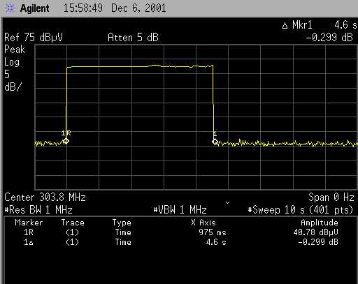
S & A Systems Fleetwatch Series TRM303 Transceiver Version 1.0.0 Operational Overview December 4, 2001 Operational Overview The TRM303 is controlled by a Microchip PIC16F876-04I/P RISC microcontroller. When instructed by serial command, the unit emits a beacon signal designed to trigger a Fleetwatch Electronic Trip Recorder. This beacon signal is a 4.25 second burst consisting of a 770 Hz stream of pulses with a 25% duty cycle over the 303.875 MHz transmitter (Refer to diagram “Data Transmit Modulation Scheme”). At the end of the beacon signal, the T/R Switch connects the receiver to the antenna and the unit looks for data on the same 303.875 MHz band. A small delay (approximately 1 second) occurs between the end of the beacon signal and the beginning of the data chain coming back to the TRM. This delay is required for backwards compatibility with previous readers, which required time for the Automatic Gain Control (AGC) circuitry to readjust to read the low-power signals returned by the RF devices, as well as for the transmitter circuitry in the device being read to power up. This delay is not required by the TRM. The microcontroller waits and examines the received data line from the receiver. A serial message is sent (over the RS-232 channel) indicating whether data was received or not, and passes either the data or a code indicating why the data could not be decoded. System Overview The TRM303 circuitry consists of three principal sections: 1) Processing Circuitry 2) Power Control & Distribution 3) Transmitter/Receiver The block diagram entitled "TRM303 Block Diagram" shows how each group interacts with each other. The Processing circuitry is the heart of the system. It controls all facets of the unit and is responsible for communication, RF control, and power operations. The Power Control system provides regulated power to the system and to monitor for out of tolerance voltages. This enables the system to turn itself off in order to prevent either damage or errant operation. It is also provided with sufficient intelligence to enable the unit to shut itself down to conserve power. Note that the unit is actually responsible for turning itself on and off. There is no mechanical on/off switch. In an error condition, the unit will default off. The receiver system is responsible for accepting and multiplexing signals from the RF link. It is designed to work at 303.825 MHz in the USA, but can be easily modified to other frequencies of interest. The Transmitter circuitry is responsible for reliably sending data over the RF link. It is also designed to work at 303.825 MHz in the USA, but can easily be modified to operate at other frequencies. The circuitry is equipped to modify it’s power level on the fly, allowing it to operate under the rules/regulations specified by different countries. Processing Circuitry The processing circuitry is the “brain” of the device. It is responsible for all aspects of control and communication. The heart of the design is the microcontroller U4, a Microchip PIC16LF876. This unit is equipped with 8K of onboard flash memory, 368 bytes of SRAM, 256 bytes of EEPROM, and a UART (as well as many other peripherals). The controller receives power from a single VDD line. The line is filtered for low frequency transients by C30. Manual reset of the controller is provided by switch SW1, which grounds the /RESET line through R20/D14 combination when pressed. Reset control is also available to an external controller through the use of the RESET line on the external connector. Any voltage between approximately 0- .5V will reset and hold in reset the TRM (active low). D1 prevents any positive voltages from entering the unit. D14 is present to prevent the voltage present from the In Circuit Programming (ICP) unit from shorting it’s +5Vdc supply to the TRM303 unit’s +3.3Vdc supply and damaging either device. The processor is timed off of crystal X1 running at 3.6864 MHz. C31 and C32 provide the parallel resonant circuit for the crystal oscillator. This frequency supplies only the microcontroller and does not traverse any distance on the PC board. Command input to the microcontroller is through COM1, which is an RS-232e port. The COM port is level shifted by U3, a standard RS232 level shifter. The inputs of this device (Sipex Part #SP3222ET or equivalent) are protected from ESD to +- 15kv. C11, C12, C13, C17, and C20 provide voltage doubler circuits for the level shifting. The comm port can be powered down (except for one receiver port) to conserve battery power. Status LEDs (D9 and D11) light during communications on the Tx and Rx lines, respectively. Theses lights are on a timing circuit which causes them to stay lit past the active time (approximately ½ second). These timing circuits are made from the not gates of U5(gates A,D, E, and F), diodes D3 and D8, capacitors C18 and C25, and resistors R12 and R15. The timing circuits work identically for both Tx and Rx. The Tx signal enters gate F of U5 and is inverted. This produces a normally low signal. When the Tx signal goes active (low), a high is produced. This voltage flows through D3 and charges (very rapidly) C18. This voltage is then re- inverted by U5A, producing a low which allows current to flow through the current limiting resistor R16, through the status LED D9 (thus lighting it), grounded into the output of U5A. When the Tx signal goes back high, the voltage on C18 slowly discharges through the parallel resistor R12 (according to the RC time constant). D3 prevents the voltage on C18 from being shunted back through the output of U5F. When the C18 voltage discharges to a sufficiently low voltage, the LED (D9) is turned back off. In this way, even fast communication signals will trigger a viewable pulse on the LED. Connection to the outside world is made by a shielded RJ45 jack (CONN1). This connection provides for Tx, Rx, and the standard RTS/CTS lines. A test connector (CONN3) provides for quick input/tap capabilities…
Text truncated - open the document above for the full version.
Schematics
123456 A B C D 6 54321 D C B A 1 S&A Systems, Inc. 992 Sid's Rd. Rockwall, TX 75032 USA 2 TRM3031.01 15-Nov-200118:20:30John Elliott Title Size:Number: Date:Drawn By: Revision: Sheetof Time: B TRM303 303.825MHz Transceiver Module Tx Rx Ctrl0 Ctrl1 Attn0 Attn1 Attn2 Attn3Attn4 RF Circuitry RF Circuitry.sch Vin 1 GND 2 Vout 5 ByPass 4 On/OFF 3 U6 LP2985 C28 10uF C27 100pF C29 .01uF GND GNDGNDGND C23 2.2uF +3V L6 2506033017ZOD +3V C30 .1uF GND X1 3.6864 MHz C32 12pF C31 12pF GNDGND C11 .1uFC17 .1uF C13 .1uF C12 .1uF C20 .1uF +3VGND GND GND +3V RB0/INT 21 RB1 22 RB2 23 RB3/PGM 24 RB4 25 RB5 26 RB6/PGC 27 RB7/PGD 28 MCLR 1 Vss 19 RA0/AN0 2 RA1/AN1 3 RA2/AN2/Vref- 4 RA3/AN3/Vref+ 5 OSC1/CLKIN 9 OSC2/CLKout 10 RA4/T0CKI 6 Vdd 20 Vss 8 RA5/AN4/SS 7 RC0/T1OSO/T1CKI 11 RC1/T1OSI/CCP2 12 RC2/CCP1 13 RC3/SCK/SCL 14 RC4/SDI/SDA 15 RC5/SDO 16 RC6/TX/CK 17 RC7/RX/DT 18 U4 PIC16LF876-04I/SP 56 U5C 74VHC04M Yellow D12 LTL-907YKTA R8 220 C21 .01uF GND VCC +3V 34 U5B 74VHC04M +3V R13 220 Red D10 LTL-907PKTA R19 330 Green D13 LTL-907LKTA GND C26 100pF 98 U5D 74VHC04M 1110 U5E 74VHC04M 12 U5A 74VHC04M 1312 U5F 74VHC04M D6 BAT54LT1 +3V R18 220 +3V R16 220 Green D9 LTL-907LKTA Green D11 LTL-907LKTA D3 BAT54LT1 D8 BAT54LT1 C18 1uF C25 1uF R12 620K R15 620K GND GND GND GND VDD 17 GND 16 V+ 3 V- 7 T1 In 12 T2 In 11 R2 Out 10 R1 Out 13 C1+ 2 C1- 4 C2+ 5 C2- 6 T1 Out 15 T2 Out 8 R1 In 14 R2 In 9 SHDN 18 EN 1 U3 ADM3222ARW D5 BAT54LT1 R14 51K GNDGND 1 2 JP1 Always On R11 4.7K 1 2 CONN4 22 11 2022 GND C22 100pF GND D4 BAT54LT1 C19 100pF GND GND GND GND 9V Bat + 9V Bat - Battery Connector GND OUT 1 Vdd 2 Gnd 3 U7 MCP120T-450I/TT GND R17 100K +3V 4.25~4.5V Trigger D2 BAV70LT1 3.3V Output Power On Indicator 1 2 3 4 5 6 7 8 9 10 CONN1 RJ45 AMP 556591-1 Shield Shield Gnd Power Pwr On from DTR Tx Out Rx In To Ring Indicator/Data Ready From RTS/Spare Input C10 100pF GND C24 1uF GND Reset RF Tx RF Rx Comm Tx Comm Rx R20 100K +3V SW1 KT11B0JM GND D1 BAT54LT1 RF_Rx RF_Tx D7 BZX84C3V0ZX DB9 Pin 5 2 3 4 9 7 D14 BAT54LT1 Shield Shield 1 2 3 4 5 6 7 8 CONN3 Test Connector Gnd Power Pwr On from DTR Tx Out Rx In To Ring Indicator/Data Ready From RTS/Spare Input Reset GND DB9 Pin Color Pin 2 - Green Pin 3 - Yellow Pin 4 - Black Pin 5 - Blue Pin 7 - White Pin 9 - Brown +12V - Orange Reset - Red DB9-RJ45 CUI Connector 123456 A B C D 6 54321 D C B A 2 S&A Systems, Inc. 992 Sid's Rd. Rockwall, TX 75032 USA 2 TRM3031.01 15-Nov-200118:20:32John Elliott Title Size:Number: Date:Drawn By: Revision: Sheetof Time: B TRM303 303.825MHz Transceiver Module Rx Tx Ctrl0 Ctrl1 Attn0Attn1 R7 51K Attn2 Output Power is Minimum at 278K, .25mW @ 11K Attn3 R2 100 Attn4 RF1 16 RF2 9 GND 10 GND 11 GND 12 GND 13 GND 14 GND 15 GND 1 GND 2 GND 8 16dB 3 8dB 4 4dB 5 2dB 6 1dB 7 U1 AA101-80 C14 100pF GND R1 10K C4 100pF GND C7 100pF GND GND GND GND GND GND R6 10K R5 100K GND GND R9 300K GND RF1 C9 100pF RF2 L1 2506033017ZOD RF3 RF4 GND RF5 C16 .1uF RF6 R4 270K R3 1.1 Meg GND C8 10uF +3V +3V RFIO 20 GND 3 19 GND1 1 VCC 1 2 CNT RL0 18 CNT RL1 17 VCC 2 16 P WIDTH 15 P RATE 14 THLD 1 13 THLD 2 12 RREF 11 GND 2 10 AGC CAP 3 PK DET 4 BB OUT 5 CMP IN 6 RX DATA 7 TX MOD 8 LPF ADJ 9 U2 TR3003 GND GND GND GND GND C2 100pF C1 100pF C3 100pF C5 100pF C6 100pF L2 82nH L5 33nH L4 82nH GND Cntrl0Cntrl1Mode 0 1 0 0 1 1 0 1Receive ASK Tx OOK Tx Sleep R10 1 MEG GND Shield 2 Shield 3 Shield 4 Shield 5 Center 1 CONN2 SMA STRAIGHT C15 15pF GND L3 33nH GND Do Not Stuff Do Not Stuff
Test Report
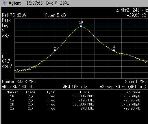
S&A Systems, Inc. Application For Certification (FCC ID: J4CTRM303) Fleetwatch TRM 303 INTERTEK TESTING SERVICES FCC ID: J4CTRM303 i LIST OF EXHIBITS INTRODUCTION EXHIBIT 1 :General Description EXHIBIT 2 :System Test Configuration EXHIBIT 3 :Emission Results EXHIBIT 4 :Equipment Photographs EXHIBIT 5 :Product Labelling EXHIBIT 6 :Technical Specifications EXHIBIT 7 :Instruction Manual EXHIBIT 8 :Miscellaneous Information INTERTEK TESTING SERVICES FCC ID: J4CTRM303 ii MEASUREMENT/TECHNICAL REPORT S&A System, Inc. - MODEL: Fleetwatch TRM 303 FCC ID: J4CTRM303 November 26, 2001 This report concerns (check one:)Original Grant X Class II Change Equipment Type: Low Power Transceiver (example: computer, printer, modem, etc.) Deferred grant requested per 47 CFR 0.457(d)(1)(ii)?Yes No X If yes, defer until: date Company Name agrees to notify the Commission by: date of the intended date of announcement of the product so that the grant can be issued on that date. Transition Rules Request per 15.37?Yes No X If no, assumed Part 15, Subpart C for intentional radiator - the new 47 CFR [10-1-96 Edition] provision. Report prepared by:Sudesh Kamble Intertek Testing Services 420 N Dorothy Drive Richardson, TX USA Phone: 972-238-5591 Fax:972-238-1860 INTERTEK TESTING SERVICES FCC ID: J4CTRM303 iii Table of Contents 1.0 General Description..................................................................................... 2 1.1 Product Description .................................................................................... 2 1.2 Related Submittal(s) Grants ........................................................................... 2 1.3 Test Methodology ...................................................................................... 3 1.4 Test Facility ............................................................................................. 3 2.0 System Test Configuration............................................................................. 5 2.1 Justification .............................................................................................. 5 2.2 EUT Exercising Software ............................................................................. 5 2.3 Special Accessories..................................................................................... 5 2.4 Equipment Modification ............................................................................... 6 2.5 Support Equipment List and Description ........................................................... 6 3.0 Emission Results......................................................................................... 8 3.1 Field Strength Calculation............................................................................. 9 3.2 Emission Configuration Photograph ................................................................10 3.3 Emission Data..........................................................................................11 4.0 Equipment Photographs...............................................................................19 5.0 Product Labelling.......................................................................................21 6.0 Technical Specifications...............................................................................23 7.0 Instruction Manual.....................................................................................25 8.0 Miscellaneous Information............................................................................27 8.1 Measured Bandwidth..................................................................................29 8.2 Discussion of Pulse Desensitization ................................................................30 8.3 Calculation of Average Factor.......................................................................31 8.4 Emissions Test Procedures...........................................................................32 INTERTEK TESTING SERVICES FCC ID: J4CTRM303 iv List of attached file Exhibit typeFile DescriptionFilename Test ReportTest Reportreport.doc Operation DescriptionTechnical Descriptionoperation desc.pdf Test Setup PhotoRadiated EmissionRconfig photos.doc Test ReportBandwidth Plotbw.gif External PhotoExternal PhotoIntrnal_external.doc Internal PhotoInternal PhotoIntrnal_external.doc Block DiagramBlock Diagramblock.pdf SchematicsCircuit Diagramcircuit.pdf ID Label/LocationLabel Artwork and Locationlabel.pdf User ManualUser Manualmanual.pdf Timing DiagramTiming Diagramtiming.gif A FCC ID: J4CTRM303 1 EXHIBIT 1 GENERAL DESCRIPTION A FCC ID: J4CTRM303 2 1.0 General Description 1.1Product Description The TRM303 printed circuit board is a transceiver module designed to allow command and control devises, such as PC, access to the M292/M392/M492 series of electronic trip recorders and other compatible Fleetwatch RF Data Acquisition equipment. It provides either for battery operated or wall power operated modes and is equipped with a standard RS-232E serial connection to facilitate communications. The device is envisioned as being used directly connected to a standard PC or as an add-on extension for hand held computing device such as the Palm III. It may also be connected to dedicated monitoring equipment for remote monitoring and recording. For electronic filing, the brief circuit description is saved with filename: descri.pdf 1.2Related Submittal(s) Grants This is a single application for certification of a transmitter. A FCC ID: J4CTRM303 3 1.3Test Methodology Radiated emission measurements were performed according to the procedures in ANSI C63.4 (1992). All measurements were performed in 3meters FCC approved Anechoic Chamber. The site attenuation of the chamber is performed as per the procedure detailed in ANSI C63.4-1992-Alternate Test Site and is within the specified tolerance. For each scan, the procedure for maximizing emissions in Appendices D and E were followed. All Radiated tests were performed at an antenna to EUT distance …
Text truncated - open the document above for the full version.
Test Setup Photos
Conducted Emission Photos FCC ID: J4CTRM303 Radiated Emission Photos
Contact Information
Applicant
John Elliott(Systems Engineer)
972-722-1009Fax: 972-722-1033
Technical Contact
S & A SystemsJohn Elliott
[email protected](972)722-1009
992 Sids Road · Rockwell, Texas · United States
Non-Technical Contact
S & A SystemsJohn Elliott
[email protected](972)722-1009
Test Firm
Intertek Testing Services NA, Inc.Sudesh Kamble
Technical Specifications
| # | Rule Parts | Frequency Range | Power Output |
|---|---|---|---|
| 1 | 15C | 303.875 MHz - 303.875 MHz | - |
Other Applications from S&A Systems Inc

J4CGPT-3
Aug 12, 2003Global Positioning Transceiver
Equipment Class
DXT - Part 15 Low Power Transceiver, Rx VerifiedJ4CM392-303
Aug 31, 1997Odometer/Trip Data Transmitter
Equipment Class
DXX - Part 15 Low Power Communication Device TransmitterJ4CMR392
Jun 02, 1997Interrigator Transmitter w/Serial Port
Equipment Class
DSC - Part 15 Security/Remote Control TransmitterJ4CFLEETWATCH-M5X
Dec 21, 1992Mobile Data Acquistion Unit
Equipment Class
DSC - Part 15 Security/Remote Control TransmitterJ4CFLEETWATCH-RFH
Aug 25, 1992Electronic Hub Odometer
Equipment Class
DSC - Part 15 Security/Remote Control Transmitter