JCA-CPAV02HUHF FM Tone and Voice Paging Receiver
SCA Inc.
Click to zoom
Application Details
- Equipment Class
- CXX - Communications Rcvr for use w/ licensed Tx and CBs
- Date of Grant
- Oct 14, 1999
- Application Purpose
- Original Equipment
- Date of Application
- Sep 12, 1999
- Equipment Note
- UHF FM Tone and Voice Paging Receiver
- Frequency Range
- 453.00000000 - 463.00000000
- Company
- SCA Inc.
- Country
- United States
Documents & Files
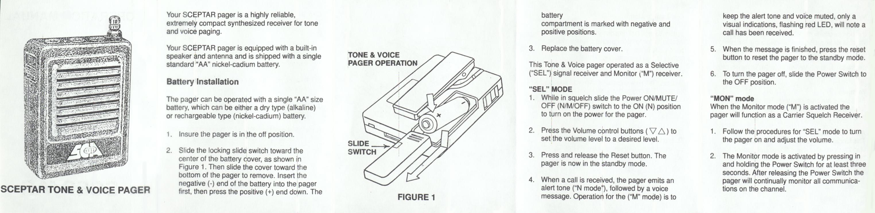
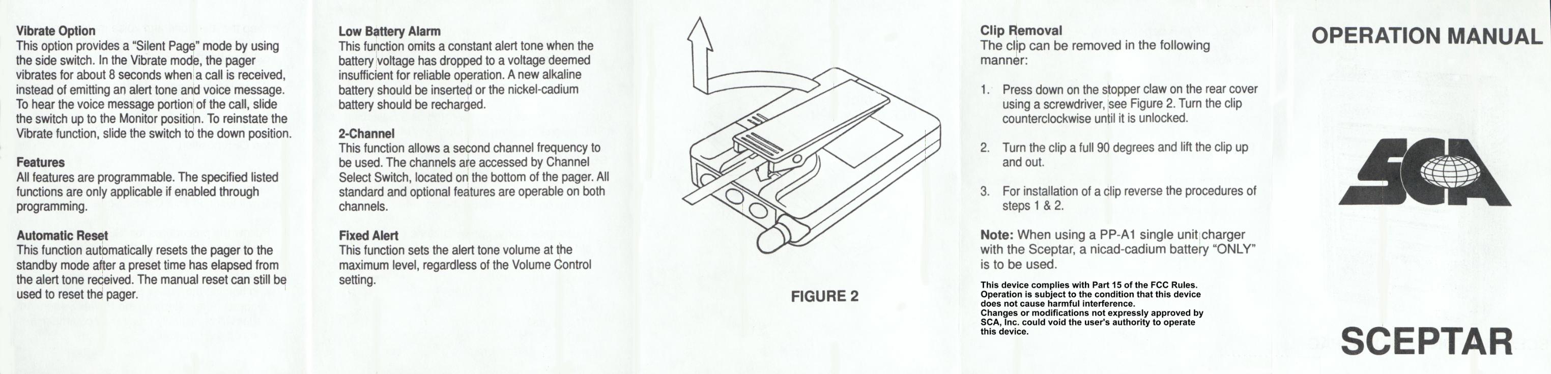
Document Text
Text extracted from the exhibit documents filed with the FCC. Open a document above to read the original.
Attestation Statements
Name and Address of the Manufacturer For the Following FCC ID”s: JCA- CPAV02M JCA- CPAV02H JCA- CPAV02HH E & M Co., Ltd. 3-6-1, EKIHIGASHI, KOKUBUNJI-MACHI, SHIMOTSUGA-GUN,TOCHIGI, JAPAN Telephone 81-285-40-1371 Facsimile81-285-40-1375
Attestation Statements
Here is process to explain how to modify Sceptar UHF(CP-AV02) A. The reason why Sceptar UHF emits spurious For lack of via holes on the ground pattern of PCB RF amplifier emits abnormal oscillation at the range of 2GHz. B. Measure By adding Via holes on the ground pattern of PCB it stabilized the circuit. C. Process of modification To take off spurious, we added 16 through holes on the PCB. See the attached photo Page 1. You can check 16 holes, which are marked by red circles. Especially the hole indicated by red arrow (See page1 below it is located near RF amplifier transistor) is very efficient to the spurious. The holes indicated by red circles are drilled 0.5mm wide in diameter. --------------------------------------- Note: 1. There is no change on the used parts on the PCB and the circuit pattern 2. The PCB has not been remade from the beginning The PCB has been modified as attached doc. Page 2 Page 2 explained how to modified PCB of Sceptar UHF.
Internal Photos
1. Drill a hole 0,5mm wide in diameter. 2. Take off solder registry to expose copper foil. 3. Thread 0.2mm wide copper line to connect both PCB. 4. Solder the copper line with PCB.
Operational Description
CIRCUIT DESCRIPTION UHF - BAND The paging receiver circuit is composed of 15 main sections: 1. Antenna circuit 9. HPF 2. RF amplifier 10. Squelch 3. SAW filter 11. Audio volume 4. PLL IC 12. AF PA 5. Loop filter 13. Decoder 6. VCO 14. D/D, Driver IC 7. First mixer 15. EEPROM 8. IF IC 1. Antenna Circuit The loop antenna ( ANT 1, ANT 2 ) and telescoping antenna ( ANT 3 ) are built into the pager and are designed to receive the UHF – band signals. The tuning frequency is automatically adjusted by the control voltage obtained from the PLL IC ( A3 ). The antenna loop is adjusted by CV1 and the telescoping antenna is a pre – select tuned circuit for the designated band. 2. RF amplifier The RF signal couples through C6 to the input of the cascade amplifier ( Q1, Q2 ). The amplified signal from Q2 passes through C10 to the SAW filter ( FL1 ). 3. SAW filter FL1 is the wide band SAW ( Surface acoustic wave ) filter. The bandwidth will be 10MHz to 11MHz, which will cover one of the bands. The unwanted frequency will be attenuated fully by this SAW filter. 4. PLL IC ( A3 ) The receiving frequency is determined by the data supplied from the decoder CPU ( A202 ). The control voltage is obtained by comparing the VCO local oscillator frequency and the 12.8MHz reference oscillator frequency. 5. Loop filter The control voltage from A3 is supplied to the loop filter via a analog switch ( A4 ). The loop filter consists of R21, R22, R23, C35, C36, and C37 which eliminates unwanted high frequency interference. 6. VCO The oscillator frequency is regulated by the control voltage and is supplied to the multiplier circuit through the buffer circuit. The oscillator frequency is set to ½ of its 1 st local frequency. 1 st local frequency = receive frequency - 21.6MHz. 7. First mixer The amplified RF signal and the injection signal in the VCO are fed into the 1 st mixer ( Q3 ). Two signals are mixed with the resulting 21.6MHz and fed into the crystal filter ( FL2 ). 11 8. IF IC ( A1 ) The IF IC consists of: 2 nd oscillator, 2 nd mixer, IF amplifier, demodulator, filter amplifier, voltage regulator, and LVA ( low – voltage – alarm ). A) 2 nd oscillator The 2 nd oscillator circuit consists of a series resonate quartz crystal ( 21.145MHz ) and IC ( A1 ). B) 2 nd mixer The output signal ( 21.6MHz ) from FL2 and the output signal ( 21.145MHz ) from the 2 nd oscillator are mixed for a resulting signal of 455KHz. C) IF amplifier / demodulator The output of the 2 nd mixer is routed through a ceramic filter ( FL3 ), internal IF amplifier, and demodulator stages D) Filter amplifier After demodulation, the audio signal is fed into the HPF ( for tone and voice ) and the BPF ( for noise amp. ). The output signal of the HPF is fed into the LPF consisting of R50, R51, R52, C65, C66, C67, and the internal filter amplifier of A1. The LPF attenuates and filters frequencies over 3KHz. E) Comparator The filtered signal is then converted to a digital signal, the output is on A1 pin 15. F) Voltage regulator The battery voltage is regulated by A1 and Q7. The voltage regulator supplies 1.0V to the receiver circuit. G) LVA The LVA circuit produces a low battery signal to the decoder CPU ( A202 ) when the battery voltage drops below 1.1 volts 9. HPF The high pass filter ( HPF ) consists of A2, C62, C63, C64, R42, R43, and R44 which eliminate the CTCSS tones from being amplified by the audio circuitry. 10. Squelch The squelch circuit consists of the BPF ( A2 – D / A, C51 thru C56 and R27 thru R30 ), noise amplifier ( Q8, Q9 ), and detector ( Q10 thru Q13 ). The squelch sensitivity is controlled by variable resistor RV1. 11. Audio volume The audio signal is controlled by R105 and R106 thru R108 in 4 audio volume levels. The output of audio signal is supplied by the AF PA through the buffer amplifier ( Q106 ). 12. AF PA The audio IC ( A102 ) and associated components form a complementary amplifier circuit for the alert tone and voice message. Transistors Q108 and Q109 provide additional current handling for driving the speaker SP1. 12 13. Decoder The decoder consists of two clock oscillators ( A104, A105 ), tone detector module (A201 ), and CPU ( A202 ). A) Clock oscillator The pager operates with two clock oscillator circuits. The main clock circuit frequency is 1.2288MHz and is controlled by A202 pin 16. When the pager is operating with the battery save function, the main clock oscillator is stopped for a period of time and the pager is in the “SAVE” mode. The SUB clock circuit oscillates continuously and provides a means for the internal timer operation. B) Tone detector ( A201 ) The tone detect module ( A201 ) consists of a alert generator circuit and tone detector circuit. C) CPU ( A202 ) The CPU will control various functions based on the EEPROM such as, tone parameter setting to detector IC ( A201 ), frequency parameter setting to the PLL IC ( A3 ), various switching operations, and the CPU output of the detector IC and timing of ESGA and ESGB. 14. D/D, Driver IC The regulated 3.0V is developed through L101 and the associated voltage multiplier circuitry in the A103. The voltage multiplier drives a switching circuit which sends pulses to L101. D102 rectifies the pulses and C109 filters them generating a regulated 3.0V. This is distributed to the decoder IC ( A201, A202 ), EEPROM ( A101 ), clock oscillator ( A104, A105 ), and PLL IC ( A3 ). A103 provides the functions for the LED ( D101 ) and vibrator ( MR101 ) option. 15. EEPROM The EEPROM ( A101 ) will retain all programmed information such as: channel frequencies, tone frequencies, tone combinations, alert cycles, scan, timing, and etc... When the paged is turned “ON”, A202 will detect the required information from the EEPROM. 13
Schematics
470 10K 68K 0.1 C49 0.1 BQ-200 0.5P C4 J1 SGSS-S06-NZ0010-GT NJU7004V A2 J2 SGSS-S07-NZ0010-GT SM5160CM 910111213141516 A3 TEST FR FV DOA DATA CLK LD VDD2 VDD1FINVSSDOP LE VDD3XOUTXIN C8 FL1 (NSVA) TA31145FN A1 1999/08/30 1P 2P 2P C14 3P 4P 5P 5P C12 4P 3P 1000P 1000P 1000P C4 - 15n 15n 15n 15n L10 100K33n0.33u 47n 18n 7P7P62P56P18P3P0.5P3P3P2P - 3P 0.5P 2P3P 3P L BAND (420-430 MHz) 0.82 L1 2SC4228 L2 2200P C84 1P100K 33n 0.33u 47n 15n 8P7P62P56P22P 3P13P 3P 3P R13 L1 L9 68K 100K 33n 33n L7 L2C33C27C24C23C21C82 C10C6 C85C2 C5 CP-AV02 0.33u 0.33u 56n 47n 18n 15n 9P 9P 8P 7P 62P 62P 56P 56P 20P 27P - 1000P - 3P3P 0.5P - 0P C1 3DC-E126Z-R1 0.68u L14 680 R8 0.01 C46 +3Vline 100K R56 C82 - C83 100K R3 R1 1SV229 - D1 D2 - D6 6543217654321 (12.8MHz) BQ-186 X2 47u C81 10K R54 1u L12 1K 10u 100K R2 455C40 CDBM FD1 CFWM455E FL3 44.545MHZ X1 (45MHz) 45M09AA4 FL2 1u L11 15n L10 0.33u L9 3.9u L8 L7 10u L6 3.3u L5 3.3u L4 18n L3 * L1 ANT3 ANT1 ANT2 47K 4.7K 1K 10K 470 10K 2.2K 470 1M 150K 2.7M 62K 11K 10K 33K 47K 330K 220K 1M 100K 47K 3.3K 47K 1M 100K 50K RV1 680K 120K 10K 220K 27K100K 68K68K 3.3K 22K 2.2K 1K 3.3K 10K 18n 10 470 4.7K 100K 10u 100K 0.22u 10u 10P 0.010.01 20P 1000P1000P 0.01 6P 2P 0.01 6P 0.01 1000P 100P 10P 30P33P 0.1u/35V 1u 0.1u/35V 270P 270P 100P100P 43P 100P 56P 100P 1000P 220P 3300P3300P3300P 8200P 10u 10u 1000P1u 0.01 0.01 8200P 100P 1200P 10u 36P 36P 1000P 4P 4P 0.01 0.01 1000P 10P 2200P 2200P 1000P 3P 2SB624 2SC4228 2SC4228 2SC4226 1SV217 1SV217 TC7S66FU DTC115TUA 2SA1576A DTC115TUA 2SC4081 2SC4081 2SC4081 2SC4081 2SC4228 2SC4228 MA111 1SV229 CV2 CV1 CV3 A4 5 4 321 87654321 11 201918171615141312 10987654321 10 9 8 7 6 5 3 2 1 12 13 14 A2-B A2-C A2-A A2-D Q14 Q13 Q12 Q11 Q10 Q9 Q8 Q7 Q6Q5 Q4 Q3 Q2 Q1 D5 D4 D3 D7 C72 C71 C70 C69 C68 C67 C66 C65 C64C63 C62 C61 C60C59 C58 C57 C56 C55 C54 C53 C52 C51 C50 C48C47 C45 C44 C43 C42 C41C40 C39 C38 C37 C36 C35 C34 C33 C32C31 C30 C29 C28 C27 C26 C25 C24 C23 C22 C21 C20 C19 C18 C17 C16 C15 C14 C13 C12 C11 C10 C9 C8 C7 C6 C3 C85 C2C5 1V AF SQ GND 3V LVA RXD BSV BATT LE DATA CLK LD R53 R23 R22 R21 R13 R14 R15 R16 R17 R18 R19 R20 R26R27 R28 R29 R30 R31 R33 R32 R34 R35 R36 R37 R38 R39 R40 R48 R47 R46 R45 R44 R43 R42 R41 R50R51R52 R25 R24 R12 R10 R11 R9 L13 R7 R6 R5 R4 R55 RX SCHEMATIC DIAGRAM 463 - 473MHz 453 - 463MHz 443 - 453MHz 420 - 430MHz FL1 2P FREQUENCY (MHz) HH BAND (463-473 MHz) H BAND (453-463 MHz) M BAND (443-453 MHz) 1000P 3P 13P 3P 5P 2P 22P 56P 62P 7P 8P - 33n 15n 47n 100K MARK:FREQUENCY SENSITIVE COMPONENTS *
Test Report
CERTIFICATION UHF-FM Tone and Voice Paging Receiver UNDER CFR 47, PART 15.109 GRANTEE: SCA, INC. FCC ID: JCA-CPAV02M FCC ID: JCA-CPAV02H FCC ID: JCA-CPAV02HH September 13, 1999 Prepared By: Spectrum Technology, Inc. 209 Dayton Street Edmonds, WA 98020 425 771-4482 CERTIFICATION TABLE OF CONTENTS Field Strength of Radiated Emissions Discussion Part 15.109(a) 1 - 2 Antenna Factors and Sample Calculations 3 - 6 Test Equipment List7 TEST: FIELD STRENGTH OF RADIATED EMISSIONS Grantee:SCA, Inc.Model:UHF-FM SCEPTAR Tone and Voice Pager FCC ID’s: JCA-CPAV02M,M band 443 – 453 MHz JCA-CPAV02H, H band453 – 463 MHz JCA-CPAV02HH,HH band463 – 473 MHz Setup: The equipment under test (EUT) was configured and operated in accordance with the applicable provisions of ANSI C63.4-1992, Section 6, 12. Measurements were made in accordance with applicable paragraphs of Section 8.2.3, Section 12.1.1.1 Appendix D, Section 12.1.4 and Appendix H3 and H4. The EUT was placed on a 1 by 1.5 meter table located 40 cm above a 2 meter diameter non-metallic turntable that sits 40 cm above the 15 X 30 meter ground plane at Spectrum's Open Area Test Site. The bi-conical or log-periodic antenna was mounted on a tower spaced at a three meters distance, and arranged for adjustment in height (1-4 meters) and vertical/horizontal polarization to maximize the emissions levels when combined with turntable rotation of the EUT. The dual ridged guide antenna was mounted on a tripod at one-meter height and adjusted for vertical or horizontal antenna orientation. A HP 8562A spectrum analyzer with a HP 8447F, Option H64 amplifier and a HP 83006A pre-amplifier were used for the peak measuring instrumentation. Discussion: Preliminary measurements were made and marginally excessive levels were observed near 2 GHz. The samples were returned to and modified by manufacturer. Please refer to the manufacturer statement regarding modification made to reduce harmonics with excessive levels just under 2 GHz. The balance of this report refers to the final set of preliminary and final measurements made to the modified units. The EUT is an UHF-FM Tone and Voice paging receiver. The receiver was powered with a single new AAA 1.5 Volt battery during measurements. Two sets of measurements were made for each of the three sample receivers tested covering the 10 MHz wide frequency bands of operation as shown below. The test samples were operated on the following channels during the measurements: M band 443 - 452CH 1 443.500 and CH 2 452.500 MHz H band 453 - 463CH 1 453.500 and CH 2 462.500 MHz HH band 463 - 464CH 1 463.500 and CH 2472.500 MHz Preliminary measurements were made as described in Section 8.3.11 and 12.1.4.1 with the receiver operating as described. The receiver was observed while positioned in three mutually orthogonal planes during which it appeared that the horizontal position, with the display facing upward, as the "worst case" position by a small margin. Page 1 During preliminary measurements numerous emissions were detected with the use of an HP 8447F amplifier and placing the receive antenna in immediate proximity of the EUT. Using a HP 83006A amplifier and moving in to less than 50 cm EUT to antenna distance for frequencies from 1 to 2 GHz, no harmonics emissions were observed. The EUT placement on the table is detailed in the photographs of the EUT setup. The final set of measurements as detailed in Section 8.3.1.2 and 12.1.4.2 were made as specified. RBW and VBW of 100 kHz were used for measurements below 1 GHz. Above 1 GHz peak measurements were made with a RBW and VBW of 1 MHz. The pager position used was based on the preliminary measurements with the display side facing up and the back or FCC ID label side facing down. We also endeavored to maximize emission levels of the EUT as appropriate, with rotation of the table and adjustment of antenna height and polarization. Measurements were made over the frequency range of 30 - 2000 MHz in great detail in accordance with Section 15.33. No emissions were measurable at three meters during the final detailed radiated emissions measurements from any of the six samples tested FCC Part 15.109(b) Field Strength of Radiated Spurious Emissions Final Data Grantee:SCA, Inc. 8/17/99 FCC ID’s: JCA- CPAV02M, JCA- CPAV02H, JCA- CPAV02HH Radiated Emissions Measurements By Frequency ________________________________________________________________________________ Freq Vert Horz Ant-F dBuV/m uV/m dB +/- Limit MHz dBm dBm Limit uV/m @ 3 Meters __________________________________________________________________________ No measurable emissions at three meters The antenna is a permanently attached pull up whip antenna emission were checked with antenna in both postions. No receiver antenna conducted spurious emissions measurements were made due to attached antenna. Conclusion: The SCA, Inc., FCC ID’s: JCA- CPAV02M, JCA- CPAV02H, and JCA- CPAV02HH, when operated and measured as discussed above, meet the receiver radiated spurious emissions requirements under Title 47, CFR Part 15.109(a). This receiver is not subject to the transition provisions of Part 15.37. Page 2 ANTENNA FACTORS FOR EMCO 3104 BICONICAL ANTENNA AND EMCO 3146 LOG PERIODIC ANTENNA INCLUDING CONVERSION TO OPEN CIRCUIT VOLTAGE. Antenna Factor and Field Strength Formula level as measured with Spectrum Analyzer converts to dBuV @ 50 ohms converts to dBuV/m dBm + 107 + AF + 6 ---- converts to open circuit uV/m = log -1 20voltage (dipole only) converts to uV/m IF FREQ => 20AND FREQ =< 26.5THEN ANTF = 12.5 IF FREQ => 26.6AND FREQ =< 28THEN ANTF = 13.5 IF FREQ => 28.1AND FREQ =< 33THEN ANTF = 14.5 IF FREQ => 33.1AND FREQ =< 35THEN ANTF = 13.5 IF FREQ => 35.1AND FREQ =< 45THEN ANTF = 13 IF FREQ => 45.AND FREQ =< 57 THEN ANTF = 12 IF FREQ => 57.1AND FREQ =< 63THEN ANTF = 11 IF FREQ => 63.1AND FREQ =< 66THEN ANTF = 10 IF FREQ => 66.1AND FREQ =< 75THEN ANTF = 9 IF FREQ => 75.1AND FREQ =< 83THEN ANTF = 8 IF FREQ => 83.1AND FREQ =< 86THEN ANTF = 9 IF FREQ => 8…
Text truncated - open the document above for the full version.
Contact Information
Applicant
Mildred Majors(Treasurer)
405 789-9371Fax: 405 789-9370
Technical Contact
Spectrum Technology IncRod Munro
[email protected]425 771-4482
209 DAYTON STREET · Edmonds, Washington · United States
Non-Technical Contact
SCA INCPaula Penn
[email protected]405 789-9371
Test Firm
Spectrum Technology Inc.Rod Munro
Technical Specifications
| # | Rule Parts | Frequency Range | Power Output |
|---|---|---|---|
| 1 | 15B | 453 MHz - 463 MHz | - |
Other Applications from SCA Inc.

JCA-CPAV03L
Feb 09, 2000Paging Receiver
Equipment Class
CXX - Communications Rcvr for use w/ licensed Tx and CBs
JCA-CPAV03M
Jan 23, 2000Paging Receiver
Equipment Class
CXX - Communications Rcvr for use w/ licensed Tx and CBs
JCA-CPAV03H
Jan 23, 2000Paging Receiver
Equipment Class
CXX - Communications Rcvr for use w/ licensed Tx and CBs
JCA-CPAV03LL
Jan 09, 2000CXX - Communications Rcvr for use w/ licensed Tx and CBs
Equipment Class
CXX - Communications Rcvr for use w/ licensed Tx and CBs
JCA-CPAV03HH
Nov 22, 1999Lowband Paging Monitor Receiver
Equipment Class
CXX - Communications Rcvr for use w/ licensed Tx and CBs