JFZT1802DCube Transmitter
Audio-Technica Corporation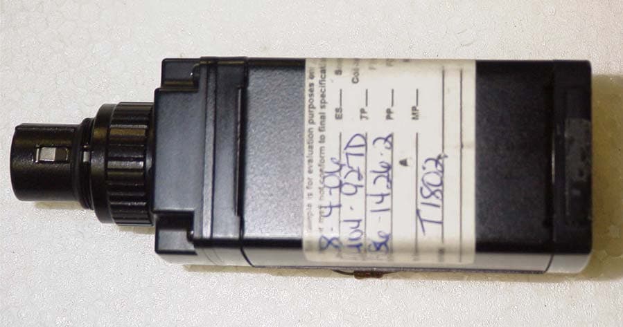
Click to zoom
Application Details
- Equipment Class
- TBF - Licensed Broadcast Transmitter Held to Face
- Date of Grant
- Oct 16, 2006
- Application Purpose
- Original Equipment
- Date of Application
- Oct 16, 2006
- Equipment Note
- Cube Transmitter
- Frequency Range
- 655.50000000 - 680.37500000
- Company
- Audio-Technica Corporation
- Country
- Japan
Documents & Files
Document Text
Text extracted from the exhibit documents filed with the FCC. Open a document above to read the original.
Cover Letter(s)
Audio-Technica U.S., Inc. 1221 Commerce Drive Phone: 330-686-2600 [email protected] Stow, OH 44224-1760 Fax: 330-688-3752 August 7, 2006 Equipment Authorization Division Office of Engineering and Technology Federal Communications Commission 7435 Oakland Mills Road Columbia, MD 21046 Ref: FCC ID: JFRT1802D Request for Confidentiality Dear Sirs: With regard to the referenced application, Audio-Technica, is requesting confidentiality of certain sections of the accompanying documents. The documents for which Audio Technica is requesting confidentiality are: 2403UT6 Block Diagram.pdf 2403UT6 Circuit Diagram 1 of 2.pdf 2403UT6 Circuit Diagram 2 of 2.pdf Block diagram for ATW-T1802 wireless transmitter This request is made under the provisions of Section 0.457(d) of the Commission’s Rules, and Section 552(b)(4) of the Freedom of Information Act. The material for which confidentiality is requested falls within the scope of Section 552(b)(4) as trade secrets and includes material covered by Section 0.459 of the Commission’s Rules. Sincerely, Jacquelynn Green Vice President R&D Audio-Technica U.S., Inc. Page 2 of 2
External Photos
AUDIO TECHNICA CORP. FCC ID: JFZT1802D EXTERNAL PHOTOS
Internal Photos
AUDIO TECHNICA CORP. FCC ID: JFZT1802D INTERNAL PHOTOS
Operational Description
Operational Description of ATW-T1802D Transmitter 1. Audio 1.1 Audio signal produced by the Microphone element is feed in to the audio IC 201. 1.2 Audio signal injected in to the IC201 is then amplified by the internal AF Amp. 1.3 Amplified audio signal is feed in to the compander circuit that const by IC251 operational amp and IC252compander IC, and compressed. 1.4 Audio signal that coming from the Guitar cable also feed in to the IC201, through the buffer amplifier, then feed in to the same AF amp listed item 1.2. 1.5 The compressed audio signal Is feed in to the IC201 and pre-emphasized and out from the IC201 and adjusted it level to appropriate by VR202. 1.6 32.15KHz signal that produced by the tone generator circuit in the IC201, is superposed with the control signal that produced by the micro-controller IC301 and out from the IC201 and adjusted it level to appropriate by VR201. 1.7 Properly adjusted Audio and tone signals are mixed and send to the VCO, VCO101. 1.8 Q201 detects peak signal level that feed in to the microphone and line input and dimmer the Power LED D303. 2. RF 1.9 RF signal produced by the VCO, VCO101 is modulate by the mixed audio and tone signal. 1.10 Modulated RF signal is through the buffer amp Q101, feed to the RF amplifier, consist by Q102 and Q103. 1.11 Amplified RF signal is then set it RF output power to; Hi position, 30mW by VR151and Low position, 10mW by VR101. 1.12 Amplified RF signal is suppress it harmonics by through Low pass filter consist by L104 to 108, C136 to 140 and feed in to Antenna terminal. 1.13 RF signal feed in to the Antenna terminal is then transmitted to the air by antenna screwed on to it.
Parts List/Tune Up Info
No. FM23-0*** Model Name ATW-T1802 ATW-T1802 Adjustment Procedure 1. Required Equipment a. Audio Signal Generator : Leader LAG-126 b. Oscilloscope : Kenwood CS-4135 c. Spectrum Analyzer : Advantest R3361A d. Modulation Analyzer : Anritsu MS616B e. Noise Meter : National VP-9680A f. DC Power Supply : Kenwood PA18-1.2A g. Multi Meter : Agilent 34401A h. RF Custom cable, BNC to MM121454 : Audio-Technica custom made RF cable 2. How to enter the Adjustment Mode 2-1 Push and hold both SW301 (SET) and SW351 (Power) together until turn the power “ON” 2-2 Push and hold both SW303 (UP) and SW302 (Down) together until “ADJ” appeared on LCD screen. 3. Adjustment 3-1 Frequency response 3-2-1 Spectrum Analyzer set up: Center Frequency 668.000MHz Frequency Span 100KHz Counter Mode ON 3-2-2 T1802 set up Frequency 668.000MHz RF HI / LOW RF HI AF Gain -6DB Lock NO.LOC MIC/INST MIC PE ON/OFF PE ON LMT. ON / OFF LMT.OFF PRESET PRESET QUIT QUIT 3-2-3 Adjustment a. Adjust the VC301 to put main carrier signal to center of the screen on spectrum analyzer. b. Adjust the VR151 to set main carrier peak leading to 120.1dBuV. c. Using power button and switch T1802 output power setting to “RF LOW” d. Adjust the VR101 to set main carrier peak leading to 115dBuV. 3-2 Pilot tone deviation level 3-3-1 Spectrum Analyzer set up Center Frequency 668.000MHz Span 100KHz Counter Mode ON DSP LINE ON, Set it to 20dBc below peak 3-3-2 T1802 set up Frequency 668.000MHz RF HI / LOW RF HI AF Gain -6DB Lock NO.LOC MIC/INST MIC PE ON/OFF PE ON LMT. ON / OFF LMT.OFF PRESET PRESET QUIT QUIT 3-3-3 Adjustment a. Adjust the VR201 to set level difference between main carrier and tone peak to 20dBc 3-3 Audio deviation level 3-4-1 Modulation Analyzer set up Deviation Sens. p-p /2 Range 40KHz HPF 50Hz LPF 3KHz Frequency 668.000MHz 3-4-2 Audio Signal Generator set up Signal Level +4dB Frequency 1KHz 3-4-3 T1802 set up Frequency 668.000MHz RF HI / LOW RF HI AF Gain -6DB Lock NO.LOC MIC/INST MIC PE ON/OFF PE ON LMT. ON / OFF LMT.OFF PRESET PRESET QUIT QUIT 3-4-4 Adjustment a. Apply audio signal from the Audio Signal Generator to the TP201 AF+ /TP203(GND) 1 b. Adjust the VR202 to set deviation to +/- 35KHz 4. Performance check 4-1 Microphone input frequency response 4-1-1 Modulation Analyzer set up Deviation Sens. p-p /2 Range 40KHz HPF 50Hz LPF 20KHz Frequency 668.000MHz 4-1-2 Noise Meter set up Response AVE Weighting WIDE 4-1-3 Audio Signal Generator set up Level -33Db Frequency 1KHz 4-1-4 T1802 set up Frequency 668.000MHz RF HI / LOW RF HI AF Gain -6DB Lock NO.LOC MIC/INST MIC PE ON/OFF PE ON LMT. ON / OFF LMT.OFF PRESET PRESET QUIT QUIT 4-1-5 Measurement procedure a. Record the Noise Meter reading and set it as reference (0dB). b. Turn the Audio Signal Generator frequency to 100Hz. c. Read the Noise meter and confirm that level difference from 1KHz reference not exceeding 0 +/- 1dB of range. d. Turn the Audio Signal Generator frequency to 10KHz. e. Read the Noise meter and confirm that level difference from 1KHz reference not exceeding +8 +/- 1dB of range. 4-2 Current consumption a. Set RF power to Hi b. Measure the current consumption by the Multi Meter and confirm that it not exceeded 230mA. c. Turn the RF power to Low d. Measure the current consumption by Multi Meter and confirm that it not exceeded 190mA
Parts List/Tune Up Info
Default PositionsPower SA Noise Meter Transmitt e Distortion M OscilloscopeVoltmeter Digital Countur SSG Local Oscillation Frequencies DC12V - 0dB 31.25kHz -20dB - - 10Hz-80MHz 1kHz CH 1 IF1=RF1-LO1=243.950MHLO2=233.250MHz CH 2 IF2=RF2-LO2=265.550MHLO2=254.850MHz Board Item SA SSG Antenn AorB Adj Point Check Point Operation Measurement Reference CH 1or2 RF TG Adjustment REF LEVEL - 1-A C1101 Input singnal to board using TG function of SA 77dBuV C1102 IC1101 11pin Adj filter with watching waveform of each □ Waveform should be f SPAN 1-B C2102 The value of 665.50 0 100MHz C2103 IC2101 11pin SA Waveform Pattern should be within ±0 . TG Input 2-A C4101 80dBuV C4102 IC4101 11pin □ Waveform level shou l 2-B C5102 ±0.5dB (It depends on adj. C5103 IC5101 11pin (Level should be th e * It is ideal that w adujsted maximum an d 655.500 668.000 680.375 RF Adj Local Oscillation Freq. Adj Local Oscillation Freq. Adj Secondary Freq. 1-A C3117 IC1201 2pin Adj with watching secondary freq. □ Adj freq. to 233.25 0 1-B - IC2201 2pin Check secondary freq. □ Check if freq. is 2 3 2-A C6117 IC4201 2pin Adj with watching secondary freq. □ Adj freq. to 254.85 0 2-B - IC5201 2pin Check secondary freq. □ Check if freq. is 2 5 Adj Primary Freq. 1-A - IC1101 8pin Check primary freq. □ 424.050MHz±0.05MHz 1-B - IC2101 8pin Check primary freq. □ 424.050MHz±0.05MHz 2-A - IC4101 8pin Check primary freq. □ 402.450MHz±0.05MHz 2-B - IC5101 8pin Check primary freq. □ 402.450MHz±0.05MHz RF Check - MOD 1-A T1201 IC1201 14pin Input modulating signal to board with SSG □ Distortion rate sho u AF distortion rate 22.5kHz 1-B T2201 IC2201 14pin Check distortion rate with putting audio s □ Distortion rate sho u RF LEVEL 2-A T4201 IC4201 14pin from each IC to distortion meter 60dBuV 2-B T5201 IC5201 14pin RF Adj RSSI - MOD 1-A VR1201 VR1201 2pin When the same strength signal is input to □ The value should be 0kHz 1-B VR2201 VR2201 2pin adj VR output for the identical voltage RF LEVEL 2-A VR4201 VR4201 2pin (Align RSSI against the same field intensity) 30dBuV 2-B VR5201 VR5201 2pin (20dBuV) (The value should b e A lignment Procedur e F Board Adjustme n ATW-R1820 f lat 0 MHz and 680.375MHz . 5dB against 668.00MHz l d be 60dBuV±3dBV jig) e same with each IC) w aveform to be d flat 0 MHz±0.05MHz 3 3.250MHz±0.05MHz 0 MHz±0.05MHz 5 4.850MHz±0.05MHz u ld be minimum u ld be within 1% 700±5mV with voltmeter e 550±5mV with voltmeter) 06/10/17
Parts List/Tune Up Info
1 2343015401 2343015501 2353009201 2353009302 2354066006 0808028604 0808189704 0808050701 2343016001 2343015701 2343015601 2343015301 2343015801 2344072401 2343016101 2353009401 2343015901 2354065901 2354041601 2354041501 0863037602 2354042101 2354045902 2354028501 2364028421 2364028341 2344073101 2369106501 1474004401 2354029301 2354027501 2354027601 2364039901 2364000461 2364000661 2364000861 9347001301 9510021201 2354066401 2354066501 235406620
Parts List/Tune Up Info
ATW-T1802 Parts List_electric PCS. P.CODEDESCRIPTION 1236910650PCB ASY-T1802-D 1236910660PCB ASY-T1802AN-D 1236910700PCB)T1802AN 1951600020C/CN)MM7329-2700-T 1971003650BP)IMSA-9120B-15 1935601820C/IC)MB1511PFV-T 1935602330C/IC)DREAMT1 1935602500C/IC)NJM2068MD-T 1935600031C/IC)NE572D 1935602390C/IC)XC61CN4002NR-T 1939600350C/VCO)T668-T 1930601210C/TR)2SC4226-24-T 2930601410C/TR)2SC5226-4-T 1930600770C/TR)2SB1295-6 1930601560C/TR)DTA114YKA-T 1930601221C/TR)2SC4738Y-T 1930601690C/TR)HN1C01F-Y-T 3922603600C/L)2520-1R0J-T 2922805670C/L)1608-FSL12NJ-T 3922805660C/L)1608-FSL10NJ-T 2922805680C/L)1608-FSL15NJ-T 1922805610C/L)1608-FSL3N9S-T 2916800520C/CS)2012-1D334M-T 4916802310C/CS)2012-1C105M-T 9916609290C/CS)2012-1A225M-T 2916800500C/CS)2012-1C225M-T 3916609310C/CS)2012-1A475M-T 1916802320C/CS)2012-0J106M-T 4916800060C/CS)3216-1A106M-T 2916603122C/CS)3528-1C106M-T 1916609250C/CS)2012-0G226M-T 1916602933C/CS)3528-0J476M-T 1916609410C/CS)7343-1C107M-T 1915801271C/CC)1608CH-1H040C-T 1915802250C/CC)1005CH-1H060D-T 1915802350C/CC)1005CH-1H330J-T 1915802370C/CC)1005CH-1H470J-T 1915802380C/CC)1005CH-1H560J-T 7915802410C/CC)1005CH-1H101J-T 3915802490C/CC)1005CH-1H471J-T 1915801561C/CC)1608CH-1H821J-T 3915802540C/CK)1005B-1H102K-T 1915802560C/CK)1005B-1H222K-T 8915802600C/CK)1005B-1E103K-T 8915805520C/CK)1005B-1C104K-T 2912600330C/CQ)2125-1C103J-T 1917600440C/CF)3225-1H473J-T 1915802200C/CC)1005CK-1H010C-T 3915802210C/CC)1005CK-1H020C-T 4915802240C/CC)1005CH-1H050C-T 11905611330C/RK)1005-000J-T 8905611340C/RK)1005-100J-T 1905611420C/RK)1005-220J-T 1905611550C/RK)1005-101J-T 3905611590C/RK)1005-151J-T 2905611620C/RK)1005-201J-T 1905611670C/RK)1005-331J-T 2905611720C/RK)1005-511J-T 5905611770C/RK)1005-102J-T 1905611840C/RK)1005-202J-T 7905611850C/RK)1005-222J-T 1905611910C/RK)1005-392J-T 2905611930C/RK)1005-472J-T 4905611940C/RK)1005-512J-T 2905611960C/RK)1005-622J-T 2905611990C/RK)1005-822J-T 6905612010C/RK)1005-103J-T 3905612600C/RK)1005-153J-T 2905612070C/RK)1005-203J-T 1905612100C/RK)1005-303J-T 6905612150C/RK)1005-473J-T 1905612210C/RK)1005-823J-T 3905612230C/RK)1005-104J-T 1905612510C/RK)1005-205J-T 3932601800C/SD)HZC6.2-T 3932601590C/SD)HSC119-T 2932600201C/SD)1SS302-T(TE85L) 1908602221C/SR)RH02B1C-223-T 1908602260C/SR)RH02B1C-101-T 1908602210C/SR)RH02B1C-104-T 1908602250C/SR)RH02B1C-103-T 1236910670PCB ASY-T1802DG-D 1236910710PCB)T1802DG 1936800410C/IC)HD64F38124WV 1935602340C/IC)NJU6366DF1-T 1935602390C/IC)XC61CN4002NR-T 1936602480C/IC)S-93C46AMFN-T 1935602400C/IC)LT1317BCMS8-T 1935602410C/IC)LM2766M6-T 1971003660BP)IMSA-9120-15 1930800350C/TR)2SA1037A K 1930601640C/TR)CPH3106-T 1930601221C/TR)2SC4738Y-T 1922603600C/L)2520-1R0J-T 1922608200C/L)1608-LK330M-T 1926800030C/L)CDRH3D23NP-100MC 2922608610C/L)2520-100K-T 1916609310C/CS)2012-1A475M-T 3916609680C/CS)3216-1A106M-T 3916609730C/CS)3216-1C106M-T 1915611380C/CK)3225B-1C106M-T 1916602933C/CS)3528-0J476M-T 2916609630C/CS)3528-0J107M-T 3916609380C/CS)3528-0J101M-T 1915802200C/CC)1005CK-1H010C-T 1915802290C/CC)1005CH-1H100J-T 3915802540C/CK)1005B-1H102K-T 1915802570C/CK)1005B-1H332K-T 5915802600C/CK)1005B-1E103K-T 8915805520C/CK)1005B-1C104K-T 5905611330C/RK)1005-000J-T 3905611550C/RK)1005-101J-T 1905611630C/RK)1005-221J-T 1905611670C/RK)1005-331J-T 2905611810C/RK)1005-152J-T 2905611940C/RK)1005-512J-T 3905612010C/RK)1005-103J-T 1905612080C/RK)1005-223J-T 1905612110C/RK)1005-333J-T 14905612150C/RK)1005-473J-T 5905612230C/RK)1005-104J-T 4905612300C/RK)1005-224J-T 1905612340C/RK)1005-334J-T 1905612440C/RK)1005-105J-T 2934800080C/LED)SML-A10MT-T 1934800060C/LED)MSL-155B6-T 1932601590C/SD)HSC119-T 4932601800C/SD)HZC6.2-T 2932600740C/SD)DCG010-T 1932601430C/SBD)SL12-E3-T 1932601600C/SBD)SB01-05Q-T 1937006870XTL)LP-3.5 9.000MHz 4948600070C/SW)SMTE3-04E-T 1918600240C/SC)TZC03R100A110 NOTES CN101 CN151 IC151 IC201 IC251 IC252 U202 VCO101 Q101 Q102,Q103 Q104 Q105 Q151 Q201 L201,L202,L203 L101,L102 L103,L104,L107 L105,L106 L108 C264,C268 C156,C201,C206,C269 C101,C202,C216,C220,C222,C227,C 251,C253,C263 C207,C208 C107,C153,C210 C270 C118,C133,C143,C211 C256,C266 C255 C104 C204 L109 C155 C254 C109 C225 C110,C102,C113,C117,C129,C132,C C214,C221,C224 C223 C105,C157,C213 C215 C106,C141,C142,C144,C145,C151,C 257,C267 C108,C154,C160,C203,C205,C212,C 217,C226 C218,C252 C265 C140 C114,C130,C139 C135,C136,C137,C138 R111,R115,R122,R152,R154,R167, R 168,R169,R171,R206,C271 R109,R153,R205,R212,R220,R226,R 257,R262 R101 R214 R104,R105,R166 R159,R222 R106 R208,R209 R110,R114,R160,R161,R253 R261 R103,R107,R151,R155,R156,R157, R R224 R170,R217 R112,R116,R163,R164 R103,R210,R260 R108,R225 R119,R120,R121,R207,R219,R252 R117,R255,R256 R113,R162 R251 R123,R165,R213,R215,R216,R221 R204 R158,R201,R203 R202 D205,D206,D207 D151,D201,D204 D251,D252 VR101 VR151 VR201 VR202 IC301 IC302 IC303 IC304 IC351 IC352 CN301 Q301 Q351 Q352 L301 L302 L351 L352,L353 C313 C301,C309,C311 C369,C370,C371 C368 C359 C365,C366 C357,C363,364 C305 C304 C353,C354,C356 C360 C302,C310,C312,C314,C351 C306,C307,C308,C323,C355,C358,C 362,C367 R317,R342,R343,R344,R345 R336,R346,R361 R302 R355 R305,R306 R353,R357 R304,R310,R351 R356 R358 R312,R318,R314,R320,R327,R328, R 329,R334,R335,R337, R338,R339,R340,R341 R311,R330,R348,R352,R354 R303,R307,R308,R309 R360 R359 D301,D302 D303 D304 D351,D352,D354,D355 D353,D356 D357 D358 XTAL301 SW301,SW302,SW303,SW351 VC301
Test Report
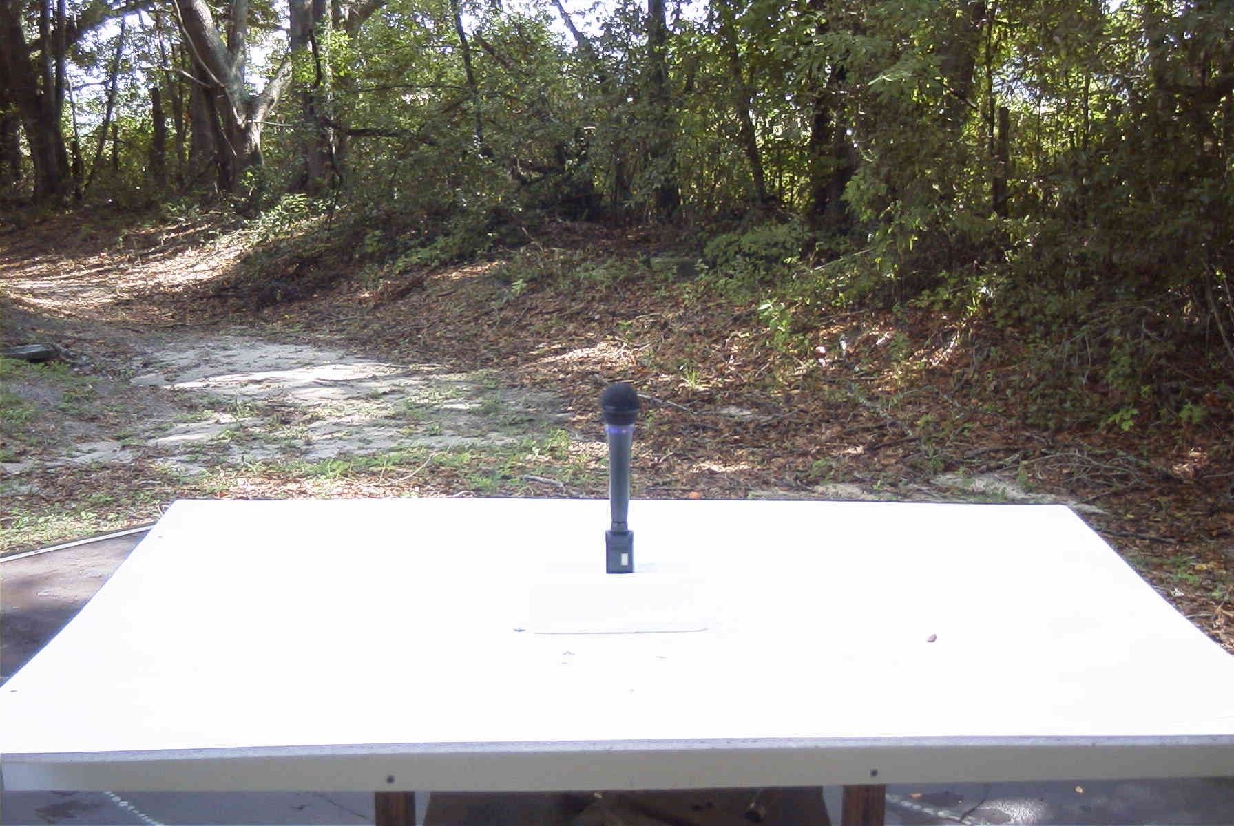
TIMCO ENGINEERING INC. A2LA ACCREDITED 849 NW State Road 45 A2LA CERT # 0955-01 Newberry, Florida 32669 http://www.timcoengr.com 888.472.2424 F 352.472.2030 email: [email protected] APPLICANT: AUDIO TECHNICA CORPORATION FCCID: JFZT1802D REPORT #: A\AudioTechnica_JFZ\2403UT6\2403UT6TestReport.doc TABLE OF CONTENTS APPLICANT: AUDIO TECHNICA CORPORATION FCC ID: JFZT1802D TABLE OF CONTENTS LIST TEST REPORT CONTAINING: PAGE 1-2........GENERAL INFORMATION PAGE 3..........RF POWER PAGE 4-5........MODULATION CHARACTERISTICS PAGE 6-7........OCCUPIED BANDWIDTH PAGE 8-10.......RADIATED EMISSIONS TEST DATA & TEST PROCEDURE PAGE 11.........FREQUENCY STABILITY TEST DATA PAGE 12-13......EQUIPMENT LIST EXHIBITS CONTAINING: CONFIDENTIALITY REQUEST LETTER FCC ID LABEL SAMPLE & ID LABEL LOCATION BLOCK DIAGRAM SCHEMATICS TUNING PROCEDURE CIRCUIT DESCRIPTION USER'S MANUAL EXTERNAL PHOTOGRAPHS INTERNAL PHOTOGRAPHS TEST SET UP PHOTOGRAPH TIMCO ENGINEERING INC. A2LA ACCREDITED 849 NW State Road 45 A2LA CERT # 0955-01 Newberry, Florida 32669 http://www.timcoengr.com 888.472.2424 F 352.472.2030 email: [email protected] APPLICANT: AUDIO TECHNICA CORPORATION FCCID: JFZT1802D REPORT #: A\AudioTechnica_JFZ\2403UT6\2403UT6TestReport.doc Page 1 of 13 GENERAL INFORMATION REQUIRED FOR TYPE ACCEPTANCE 2.1033(c)(1) AUDIO TECHNICA CORPORATION will manufacture the JFZT1802D in quantity under FCC RULES PART 74.801, 2.1033(c)(2) LOW POWER AUXILIARY STATIONS. AUDIO TECHNICA CORPORATION 2206 NARUSE, MACHIDA TOKYO, 194 JAPAN 2.1033 TECHNICAL DESCRIPTION (c)(3) Instruction book. The instruction manual is in- cluded as an exhibit. (c)(4) Type of Emission: 130K0F3E Bn = 2M + 2DK M = 20000 D = 45kHz(Peak Deviation) K = 1 Bn = 2(20k) + 2(45k)(1) = 130k ALLOWED AUTHORIZED BANDWIDTH = 200kHz. 74.861(e)(5) (c)(5) Frequency Range: Part 74: 655.500 - 680.375 MHz TEST FREQ = 655.50 MHz, 668.00MHz, and 680.375MHz (c)(6) Power Range and Controls: UNIT has no controls. (c)(7) Maximum Output Power Rating: .008 Watts ERP (c)(8) DC Voltages and Current into Final Amplifier: FINAL AMPLIFIER ONLY INPUT POWER – (3.0V)(0.0.09A) = 0.27 Watts (c)(9) Tune-up procedure. The tune-up procedure is included as an exhibit. TIMCO ENGINEERING INC. A2LA ACCREDITED 849 NW State Road 45 A2LA CERT # 0955-01 Newberry, Florida 32669 http://www.timcoengr.com 888.472.2424 F 352.472.2030 email: [email protected] APPLICANT: AUDIO TECHNICA CORPORATION FCCID: JFZT1802D REPORT #: A\AudioTechnica_JFZ\2403UT6\2403UT6TestReport.doc Page 2 of 13 2.1033 (c)(10) Complete Circuit Diagrams and Block Diagrams are included in the exhibits. 2.1033 (c)(11) Photo or Drawing of Label and sketch of location are included in the exhibits. 2.1033 (c)(12) Photos of Equipment are included in the exhibits. (c)(13) The circuit description is included in the exhibits. 2.1033 (c)(14) The data required by 2.1046 through 2.1057 is submitted below. TIMCO ENGINEERING INC. A2LA ACCREDITED 849 NW State Road 45 A2LA CERT # 0955-01 Newberry, Florida 32669 http://www.timcoengr.com 888.472.2424 F 352.472.2030 email: [email protected] APPLICANT: AUDIO TECHNICA CORPORATION FCCID: JFZT1802D REPORT #: A\AudioTechnica_JFZ\2403UT6\2403UT6TestReport.doc Page 3 of 13 2.1046 RF power output. RF power measured is: OUTPUT POWER: .008 WATTS For a device with a fixed antenna, RF power is measured as ERP as the antenna is permanently attached. The substitution method was used as described in TIA- 603-C. R.F. POWER OUTPUT TEST PROCEDURE TIMCO ENGINEERING INC. A2LA ACCREDITED 849 NW State Road 45 A2LA CERT # 0955-01 Newberry, Florida 32669 http://www.timcoengr.com 888.472.2424 F 352.472.2030 email: [email protected] APPLICANT: AUDIO TECHNICA CORPORATION FCCID: JFZT1802D REPORT #: A\AudioTechnica_JFZ\2403UT6\2403UT6TestReport.doc Page 4 of 13 2.1047(a)(b) Modulation characteristics: AUDIO FREQUENCY RESPONSE The audio frequency response was measured in accordance with TIA/EIA Specification 603. The audio frequency response curve is shown on the next page. AUDIO LOW PASS FILTER The audio low pass filter is not required in this unit. Audio Frequency Response Plot Ma xFre q .a t1 ColorLine StyleThickDataAxis CyanSolid1Anlr.Level A!Norm alizeLeft -0 +12 +2 +4 +6 +8 +10 d B 10030k2005001k2k5k10k20k Hz TIMCO ENGINEERING INC. A2LA ACCREDITED 849 NW State Road 45 A2LA CERT # 0955-01 Newberry, Florida 32669 http://www.timcoengr.com 888.472.2424 F 352.472.2030 email: [email protected] APPLICANT: AUDIO TECHNICA CORPORATION FCCID: JFZT1802D REPORT #: A\AudioTechnica_JFZ\2403UT6\2403UT6TestReport.doc Page 5 of 13 Modulation Limiting Plots: 15 KHz (Green),3.0 KHz (Blue), and 300 Hz (Yellow) 0 45.0 k H z 100500200300400 Vpp TIMCO ENGINEERING INC. A2LA ACCREDITED 849 NW State Road 45 A2LA CERT # 0955-01 Newberry, Florida 32669 http://www.timcoengr.com 888.472.2424 F 352.472.2030 email: [email protected] APPLICANT: AUDIO TECHNICA CORPORATION FCCID: JFZT1802D REPORT #: A\AudioTechnica_JFZ\2403UT6\2403UT6TestReport.doc Page 6 of 13 2.1049(c) Occupied Bandwidth: Data in the plots show that all sidebands between 50 & 100% for the authorized bandwidth are attenuated by at least 25dB. From 100 to 250% of the authorize3d band- width they are attenuated by at least 35dB and beyond 250% 43 log(Po) dB. The plot shows the transmitter modulated with 15000 Hz(the highest modulation frequen- cy), adjusted for 50% modulation plus 16 dB. The spectrum analyzer was set with the unmodulated carrier at the top of the screen. The test procedure diagram and occupied bandwidth plot follow. Wireless Microphone transmitter: Test procedure diagram OCCUPIED BANDWIDTH MEASUREMENT Transmitter Coupler 50 ohm under test Resistive Load Audio Spectrum Oscillator Analyzer REQUIREMENT: PART 74: 200kHz EMISSION BANDWIDTH. TIMCO ENGINEERING INC. A2LA ACCREDITED 849 NW State Road 45 A2LA CERT # 0955-01 Newberry, Florida 32669 http://www.timcoengr.com 888.472.2424 F 352.472.2030 email: [email protected] APPLICANT: AUDIO TECHNICA CORPORATION FCCID: JFZT1802D REPORT #: A\AudioTechn…
Text truncated - open the document above for the full version.
Contact Information
Applicant
Fumio Kamimura(General Manager, Engineering Planning Division)
Test Firm
Timco Engineering, Inc.Sid Sanders
Technical Specifications
| # | Rule Parts | Frequency Range | Power Output | Emission | Tolerance |
|---|---|---|---|---|---|
| 2 | 74.861 | 655.5 MHz - 680.375 MHz | 2.00 mW | 130KF3E | 50 ppm |
Other Applications from Audio-Technica Corporation
JFZDT3207DF2
Apr 06, 2026DESK STAND TRANSMITTER
Equipment Class
DWM - Part 15 Wireless MicrophoneJFZT210CS
Jul 17, 2024UniPak Transmitter
Equipment Class
TLD - Licensed LPAS DeviceJFZT220CS
Jul 17, 2024Handheld Transmitter
Equipment Class
TLD - Licensed LPAS DeviceJFZCKS50TW2R
Jun 10, 2024Wireless Headphones
Equipment Class
DTS - Digital Transmission SystemJFZCKS30TWPR
Apr 02, 2024Wireless Headphones
Equipment Class
DSS - Part 15 Spread Spectrum Transmitter