JFZT201Beltpack Wireless Microphone
Audio-Technica Corporation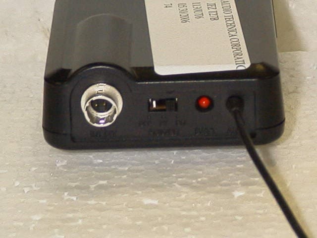
Click to zoom
Application Details
- Equipment Class
- TNT - Licensed Non-Broadcast Transmitter Worn on Body
- Date of Grant
- Oct 24, 2006
- Application Purpose
- Original Equipment
- Date of Application
- Oct 23, 2006
- Equipment Note
- Beltpack Wireless Microphone
- Frequency Range
- 169.44500000 - 171.90500000
- Company
- Audio-Technica Corporation
- Country
- Japan
Documents & Files
Document Text
Text extracted from the exhibit documents filed with the FCC. Open a document above to read the original.
Users Manual
200 Series Owners Manual v.1 7-6-06 Page 1 of 9 ATW-251 UniPak™ System ATW-251/G Guitar System ATW-251/H Headworn Microphone System ATW-251/L Lavalier Microphone System ATW-252 Handheld Microphone System This device complies with part 15 of the FCC Rules. Operation is subject to the condition that this device does not cause harmful interference. This device complies with INDUSTRY CANADA R.S.S. 210, en conformité avec IC: RSS-210/CNR210. Operation is subject to the following conditions: 1) This device may not cause harmful interference and 2) this device must accept any interference received, including interference which may cause undesired operation. CAUTION! Electrical shock can result from removal of the receiver cover. Refer servicing to qualified service personnel. No user-serviceable parts inside. Do not expose to rain or moisture. The circuits inside the receiver and transmitter have been precisely adjusted for optimum performance and compliance with federal regulations. Do not attempt to open the receiver or transmitter. To do so will void the warranty, and may cause improper operation. Notice to individuals with implanted cardiac pacemakers or AICD devices : Any source of RF (radio frequency) energy may interfere with normal functioning of the implanted device. All wireless microphones have low-power transmitters (less than 0.05 watts output) which are unlikely to cause difficulty, especially if they are at least a few inches away. However, since a “body-pack” mic transmitter typically is placed against the body, we suggest attaching it at the belt, rather than in a shirt pocket where it may be immediately adjacent to the medical device. Note also that any medical-device disruption will cease when the RF transmitting source is turned off. Please contact your physician or medical-device provider if you have any questions, or experience any problems with the use of this or any other RF equipment. 200 Series Owners Manual v.1 7-6-06 Page 2 of 9 Introduction Thank you for choosing an Audio-Technica professional wireless system. You have joined thousands of other satisfied customers who have chosen our products because of their quality, performance and reliability. This wireless microphone system is the successful result of years of design and manufacturing experience. Each 200 Series professional VHF wireless system includes a receiver and either a body-pack transmitter or a handheld microphone/transmitter on a specific crystal-controlled frequency. ATW-251 UniPak™ body-pack transmitter systems include models pre-packaged with either an AT-GCW guitar cable (/G), a PRO 8HEcW headworn microphone (/H), or a lavalier mic (/L) for particular applications. All A-T Wireless Essentials™ microphones and cables, available separately, are pre-terminated for use with any ATW-251 system. Because 200 Series packaging is designed to hold all versions of the system, some compartments in the carton are intentionally left empty. The ATW-R250 receiver includes a space-saving switching power supply that automatically adapts to changes in mains voltage. Unlike bulky linear power supplies, this switching power supply is lightweight and compact; it uses only a single outlet space. The versatile ATW-T201 UniPak body-pack transmitter has both a high- impedance input for instruments, and a low-impedance input with bias connection for use with dynamic and electret condenser microphones. The ATW- T202 handheld transmitter features a unidirectional dynamic microphone element. Both the body-pack and handheld transmitters use internal 9-volt batteries and have Off/Standby/On switches, input Trim (level) adjustments and battery-save switches. Receiver Installation Location For best operation the receiver should be at least 3' (1 m) above the ground and at least 3' (1 m) away from a wall or metal surface to minimize reflections. Keep the receiver antennas away from noise sources such as digital equipment, motors, automobiles and neon lights, as well as away from large metal objects. In multi-channel systems, position receivers at least 3' (1 m) apart and keep operating transmitters at least 6' (2 m) from the receivers to help assure maximum RF performance. Output Connection The receiver provides unbalanced, aux-level output from a 1/4" TS (“mono”) phone jack; an output cable is not included. Use a shielded audio cable with 1/4" 200 Series Owners Manual v.1 7-6-06 Page 3 of 9 phone plug to connect the receiver’s AF Out jack to the mixer/amplifier’s aux- level input. Power Connection Connect the DC plug on the included AC power adapter to the DC power input on the back of the receiver. Secure the cord over the cord hook on the back of the receiver, to keep the plug from being detached by an accidental tug on the cord. Then plug the adapter into a standard 120 Volt 60 Hz AC power outlet. (Note that the receiver has no power Off/On switch. The receiver will be energized whenever the power adapter is connected and plugged into the AC outlet. Unplug the power supply from the AC outlet when the system is not in use – both for safety, and to conserve energy.) Antennas A novel “dipole” antenna system on the receiver improves operation by providing a “ground” element in addition to the usual “signal” element. Position the two antennas at 90° in the form of a “V,” or position the left (“signal”) antenna vertically and the right (“ground”) antenna horizontally, in the shape of an “L” (Fig. B). Use the position that performs better in your operating environment. Be certain to extend both antennas to their full 15" (38 cm) length by holding them at their bases and pulling out on their caps. Both antenna elements may be swiveled to the left and right, but do not attempt to rotate them in a screwing/unscrewing motion. To do so may damage the antenna and/or receiver. For best performance, locate the receiver so its antennas are in direct line-of- sight to the transmitter’s likely operating position. Receiver Controls and Functions F…
Text truncated - open the document above for the full version.
Cover Letter(s)
Audio-Technica U.S., Inc. 1221 Commerce Drive Phone: 330-686-2600 [email protected] Stow, OH 44224-1760 Fax: 330-688-3752 September 28, 2006 Equipment Authorization Division Office of Engineering and Technology Federal Communications Commission 7435 Oakland Mills Road Columbia, MD 21046 Ref: FCC ID: JFZT201 Request for Confidentiality Dear Sirs: With regard to the referenced application, Audio-Technica, is requesting confidentiality of certain sections of the accompanying documents. The documents for which Audio Technica is requesting confidentiality are: T201 Circuit Diagram 1 of 2.pdf T201 Circuit Diagram 2 of 2.pdf T201_Block_Diagram.pdf This request is made under the provisions of Section 0.457(d) of the Commission’s Rules, and Section 552(b)(4) of the Freedom of Information Act. The material for which confidentiality is requested falls within the scope of Section 552(b)(4) as trade secrets and includes material covered by Section 0.459 of the Commission’s Rules. Sincerely, Jacquelynn Green Vice President R&D Audio-Technica U.S., Inc.
External Photos
AUDIO TECHNICA CORP. FCC ID: JFZT201 EXTERNAL PHOTOS
ID Label/Location Info
S=1/1 版下NO. 品名 FH-1741a ID SEAL P.CODE2344-07730 機種名 ATW-T201
Internal Photos
AUDIO TECHNICA CORP. FCC ID: JFZT201 INTERNAL PHOTOS
Operational Description
ATW-T201 (1) Audio PCB Audio signal from microphone capsule is input to MIC IN and AFGND. B+ is used microphone capsule which is required of power supply. Input signal from guitar cable goes into Guitar IN and AFGND. Q1 is the buffer amplifier. User arranges VR1 and VR2 input signal label. IC1 (1/2) is pre amplifier. It stays on clip if added more than 0.2V to MIC IN. Gain setting at 35dB against MIC IN (VR1 MAX) and 20dB against Guitar IN (VR2 MAX). It is available to input up to 135dB SPL on condition of audio pressure level to microphone capsule. The max level is equal to max MIC input level. It stays on clip if added more than 0.9V to Guitar IN. This level equals to MAX Guitar input level. IC1 works as a compressor combined with IC2. The D1, Q2 circuit block is a modulation limiter. C8, C21 are oscillator prevention capacitors. VR3 (10Kohm) is potentiometer which controls modulation level. When SW1 is in a position of ST, C31 and ground is shorted, and goes to mute mode. When the voltage of 9V battery lowers, D2 dims to inform the user that it is the time to change the battery. (2) RF PCB X-tal is applied for Oscillation and Modulation circuit. Q201 is sextic overtone (X6 multiplier) oscillation circuit. Oscillation by x-tal is equivalent to the oscillation circuit of series of C and L. It is set to gain the higher frequency than x-tal’s unique oscillation frequency by putting D202 that is set to reverse bias with the series of x-tal, L201, R201 and R203. Therefore, by VR201 oscillation frequency can be fine-tuned. Also by adding the sound signal to D202, D202’s capacity is changed by its voltage change and modulated. Zero temperature coefficient condenser is used in C203 and C204 in order to get the stable oscillation that is close to sigh wave against the temperature change. TL1, C205 and TL2, C208 consist of double-tuned circuit, which reduce spurious. Q202 is the transistor for frequency amplification. L203, VC1 is the circuit to tune to X2 frequency from the prior stage. L203, VC1 and L204, VC2 consist of double-tuned circuit, which reduce spurious. Q203 is the transistor for RF amplification tuned by L205 and VC3. RF output can be controlled by rotating trimmer condenser of VC1, VC2 and VC3. Supplied voltage for Q202 and Q203 is switched by SW2. It also enables to switch RF output high or low. From C217 to L208 are the filter circuit. It cuts the spurious higher than oscillation frequency and will match to antenna of T201.
Parts List/Tune Up Info
ATW-T202 (1) Audio PCB Audio signal from microphone capsule is input to AF, AFGND. B+ is used microphone capsule which is required of power supply. It connects in using of T202. User arranges VR1input signal label. IC1 (1/2) is pre amplifier. It stays on clip if added more than 0.2V, MIC in condition of gain setting at 35dB, VR1 MAX. It is available to input up to 135dB SPL on condition of audio pressure level to microphone capsule. The max level is equal to T202 max one. It works as a compressor combined with IC2 for compandor. The D1, Q2 circuit block is a modulation limiter. C6, C15 are oscillator prevention capacitors. VR2 is potentiometer and which is controlled modulation level. When SW1 is in a position of ST, BY between VR2, L4 and ground, it stays short and also mute mode. D5 is circuit protection diode in case battery connects oppositely. (2) RF PCB X-tal is applied for Oscillation and Modulation circuit. Q2 is sextic overtone (X6 multiplier) oscillation circuit. Oscillation by x-tal is equivalent to the oscillation circuit of series of C and L. It is set to gain the higher frequency than x-tal’s unique oscillation frequency by putting D4 that is set to reverse bias with the series of x-tal, L5 and R20. Therefore, by VR3 oscillation frequency can be fine-tuned. Also by adding the sound signal to D4, D4’s capacity is changed by its voltage change and modulated. Zero temperature coefficient condenser is used in C32 and C33 in order to get the stable oscillation that is close to sigh wave against the temperature change. T1, C34 and T2, C36 consist of double-tuned circuit, which reduce spurious. Q3 is the transistor for frequency amplification. L6, VC1 is the circuit to tune to X2 frequency from the prior stage. L6, VC1 and L7, VC2 consist of double-tuned circuit, which reduce spurious. Q4 is the transistor for RF amplification tuned by L8 and VC3. RF output can be controlled by rotating trimmer condenser of VC1, VC2 and VC3. Supplied voltage for Q3 and Q4 is switched by SW2. It also enables to switch RF output high or low. From C47 to L10 are the filter circuit. It cuts the spurious higher than oscillation frequency and will match to antenna of T202. When the voltage of 9V battery lowers, D2 dims to inform the user that it is the time to change the battery.
Parts List/Tune Up Info
ATW-T201(S-1) Parts List_electric A → 169.505 , B → 170.245 , C → 171.905 ABC 1236910970PCB ASY-T201US169.50 1236910971PCB ASY-T201US170.24 1236910972PCB ASY-T201US171.90 111236910960PCB)ATW-T201US 222925000230TRS)S7-T4/3960D 111235400924COL)D3-7T-0.65 1937700060XTL)HC49/U14.1151MHz 1937700070XTL)HC49/U14.1768MHz 1937700080XTL)HC49/U14.3151MHz 111915801250C/CC)1608CH-1H020C-T 111915801260C/CC)1608CH-1H030C-T 111915801270C/CC)1608CH-1H040C-T 111915801370C/CC)1608CH-1H220J-T 333920700040AL)02-1R2K-AC-T 111920700050AL)02-220K-AC-T 111920100290AL)02-3R3J-AC-T 111920100280AL)02-100J-AC-T 111900400730RD)1/6W222J-TP 333226900050JW)L5.0D0.6-TP 333226900051JW)L7.5D0.6-TP 111226900052JW)L10.0D0.6-TP 111226900053JW)L12.5D0.6-TP 111226900054JW)L15.0D0.6-TP 111226900055JW)L17.5D0.6-TP 999910703340CE)1H2R2M-TP-P2.5 111910703400CE)1HR10M-TP-P2.5 111910703350CE)1H4R7M-TP-P2.5 111910703330CE)1H1R0M-TP-P2.5 222910703410CE)1C470M-TP-P2.5 111910703320CE)NP1HR47M-TP-P2.5 111910703420CE)NP1H1R0M-TP-P2.5 222910703430CE)1HR22M-TP-P2.5 222235400833COL)D4-2R5T-0.65 111235400924COL)D3-7T-0.65 444918700010SC)TZ03T200F169B00 111908000810SR)RH0411C15J18A 333908000320SR)RH0411C 10kB 111935002660IC)UTC571N 111935001590IC)NJM2068L 111945000421SW)SSSF123-P06S-1 111945000520SW)SSSS2-12 111971001400BP)SB2P-HVQ-S 111971001810BP)SB4P-HVQ-S 111236401663WL)1571C26WH50 111934000840LED)SLP-181B-51 111235400040LEDS-LH-5-4 111930600111C/TR)2SC2712-Y-T 222930600690C/TR)2SC3123-T 111930600510C/TR)2SC3124-T 111931600170C/FET)2SK208-R-T 111932600010C/SD)1SS294-T 222932600180C/SD)DCC010-W7-T 111932600430C/VCD)1SV230-T7-T PCS. P.CODEDESCRIPTION 111932600420C/ZD)02CZ5.6-Y-T 111915801550C/CC)1608CH-1H681J-T 111915801410C/CC)1608CH-1H470J-T 222915801510C/CC)1608CH-1H331J-T 111915801700C/CK)1608B-1H472K-T 999915801720C/CK)1608B-1H103K-T 111915801330C/CC)1608CH-1H100D-T 222915805600C/CC)1608UJ-1H470J-T 111915801460C/CC)1608CH-1H121J-T 111915801450C/CC)1608CH-1H101J-T 222915801210C/CC)1608CH-1H0R5C-T 333915801310C/CC)1608CH-1H080D-T 111915801260C/CC)1608CH-1H030C-T 333915801570C/CC)1608CH-1H102J-T 111915801400C/CC)1608CH-1H390J-T 111905800744C/RK)1608-103J-T 111905800724C/RK)1608-822J-T 333905800504C/RK)1608-102J-T 111905800684C/RK)1608-562J-T 333905800664C/RK)1608-472J-T 333905800904C/RK)1608-473J-T 333905800584C/RK)1608-222J-T 111905800984C/RK)1608-104J-T 222905800864C/RK)1608-333J-T 111905800764C/RK)1608-123J-T 111905800624C/RK)1608-332J-T 111905800574C/RK)1608-202J-T 111905800484C/RK)1608-821J-T 222905801234C/RK)1608-205J-T 333905800824C/RK)1608-223J-T 111905801064C/RK)1608-224J-T 111905800304C/RK)1608-151J-T 111905800284C/RK)1608-121J-T 111905800554C/RK)1608-162J-T 111905800784C/RK)1608-153J-T 111905800404C/RK)1608-391J-T TL1,2 L206 X1 X1 X1 C214 C209 C205 C208 L1,2,3 L202 L201 L207 R15 JW1,3,10 JW7,8,9, JW6 JW2 JW5 JW4 C1,10,11,12,14,20,23,28,31 C5 C13 C15 C22,40 C7 C3 C24,26 L203,204 L208 VC1,2,3,4 VR2 VR1,3,201 IC2 IC1 SW1 SW2 CN2 CN1 D2 LED s pacer Q2 Q201,Q202 Q203 Q1 D3 D1,4 D202 NOTES ZD201 C2 C4 C9,18 C16 C17,25,27,30,32,202,206,211,221 C19 C203,204 C8 C201 C207,212 C210,215,218 C217 C216,219,220 C21 R1 R2 R4,13,16 R7 R8,23,202 R9,204,209 R10,11,206 R12 R14,19 R18 R20 R24 R3 R5,6 R201,205,17 R207 R208 R210 R22 R203 R211
Test Report
TIMCO ENGINEERING INC. 849 NW State Road 45 Newberry, Florida 32669 http://www.timcoengr.com 888.472.2424 F 352.472.2030 email: [email protected] APPLICANT: AUDIO TECHNICA CORPORATION FCC ID: JFZT201 REPORT #: V:\A\AudioTechnica_JFZ\1130UT6\1130UT6TestReport.doc COVER SHEET Test Report Product Name: BELTPACK TRANSMITTER FCC ID: JFZT201 Applicant: AUDIO TECHNICA CORPORATION 2206 NARUSE, MACHIDA TOKYO 194 JAPAN Date Receipt:5/30/2006 Report Date: 10/2/2006 TIMCO ENGINEERING INC. 849 NW State Road 45 Newberry, Florida 32669 http://www.timcoengr.com 888.472.2424 F 352.472.2030 email: [email protected] APPLICANT: AUDIO TECHNICA CORPORATION FCCID: JFZT201 REPORT #: V:\A\AudioTechnica_JFZ\1130UT6\1130UT6TestReport.doc TABLE OF CONTENTS TABLE OF CONTENTS LIST TEST REPORT CONTAINING: PAGE 1-2 GENERAL INFORMATION PAGE 3 RF POWER OUTPUT PAGE 4 MODULATION CHARAC & MOD LIMITING PLOT PAGE 5 AUDIO FREQUENCY RESPONSE PLOT PAGE 6-7 OCCUPIED BANDWIDTH PAGE 8-10 RADIATED EMISSIONS TEST DATA PAGE 11 METHOD OF MEASURING RADIATED EMISSIONS PAGE 12 FREQUENCY STABILITY TEST DATA PAGE 13-14 EQUIPMENT LIST EXHIBITS CONTAINING: CONFIDENTIALITY REQUEST LETTER FCC ID LABEL SAMPLE SKETCH OF FCC ID LABEL LOCATION BLOCK DIAGRAM SCHEMATIC TUNING PROCEDURE CIRCUIT DESCRIPTION USER'S MANUAL TEST SET UP PHOTOGRAPH EXTERNAL PHOTOGRAPHS INTERNAL PHOTOGRAPHS TIMCO ENGINEERING INC. 849 NW State Road 45 Newberry, Florida 32669 http://www.timcoengr.com 888.472.2424 F 352.472.2030 email: [email protected] APPLICANT: AUDIO TECHNICA CORPORATION FCCID: JFZT201 REPORT #:V:\A\AudioTechnica_JFZ\1130UT6\1130UT6TestReport.doc Page 1 of 14 GENERAL INFORMATION REQUIRED FOR TYPE ACCEPTANCE 2.1033 AUDIO TECHNICA CORPORATION will manufacture the 2.1034 FCC ID: JFZT201 in quantity, for use under FCC RULES PART 90.265. 2.1033 (C4) TECHNICAL DESCRIPTION (1) Type of Emission: 54KF3E Bn = 2M + 2DK M = 19000 D = 8 kHz (Peak Deviation) K = 1 Bn = 2(19k) + 2(8k)(1) = 54000 ALLOWED AUTHORIZED BANDWIDTH = 54 kHz. 90.265 (b) (2) Frequency Range: 169.445-171.905 (3) Power Range and Controls: Unit has no controls. (4) Maximum Output Power Rating: PWR: ERP 0.002 Watts (5) DC Voltages and Current into Final Amplifier: FINAL AMPLIFIER ONLY INPUT POWER – (9.0V)(0.035A) = 0.31 Watts 2.1033 (C.10)(7) Complete Circuit Diagrams: The circuit diagram and block diagram are included. (8) Instruction book. The instruction manual is included. Tune-up procedure. The tune-up procedure is included. 2.1033 (c.11) Photo or drawing of label location are included. 2.1033 (c.12) Photos of the device are included. TIMCO ENGINEERING INC. 849 NW State Road 45 Newberry, Florida 32669 http://www.timcoengr.com 888.472.2424 F 352.472.2030 email: [email protected] APPLICANT: AUDIO TECHNICA CORPORATION FCCID: JFZT201 REPORT #:V:\A\AudioTechnica_JFZ\1130UT6\1130UT6TestReport.doc Page 2 of 14 APPLICANT: AUDIO TECHNICA CORPORATION FCC ID: JFZT201 (10) Description of all circuitry and devices provided for determining and stabilizing frequency. The circuit description is included. (12) Digital modulation. This unit does not use digital modulation. 2.983(e) The data required by 2.1046 through 2.1057 is submitted below. TIMCO ENGINEERING INC. 849 NW State Road 45 Newberry, Florida 32669 http://www.timcoengr.com 888.472.2424 F 352.472.2030 email: [email protected] APPLICANT: AUDIO TECHNICA CORPORATION FCCID: JFZT201 REPORT #:V:\A\AudioTechnica_JFZ\1130UT6\1130UT6TestReport.doc Page 3 of 14 2.1046 RF Power Output. RF power is measured as effective radiated power. OUTPUT POWER: .002W ERP For a device with a fixed antenna, RF power is measured as ERP as the antenna is permanently attached. The substitution method was used. With a nominal battery voltage, and the transmitter properly adjusted the RF output measures: R.F. POWER OUTPUT TEST PROCEDURE TIMCO ENGINEERING INC. 849 NW State Road 45 Newberry, Florida 32669 http://www.timcoengr.com 888.472.2424 F 352.472.2030 email: [email protected] APPLICANT: AUDIO TECHNICA CORPORATION FCCID: JFZT201 REPORT #:V:\A\AudioTechnica_JFZ\1130UT6\1130UT6TestReport.doc Page 4 of 14 2.1047(a)(b) Modulation characteristics: AUDIO_LOW_PASS_FILTER The audio low pass filter is not required in this unit. TIMCO ENGINEERING INC. 849 NW State Road 45 Newberry, Florida 32669 http://www.timcoengr.com 888.472.2424 F 352.472.2030 email: [email protected] APPLICANT: AUDIO TECHNICA CORPORATION FCCID: JFZT201 REPORT #:V:\A\AudioTechnica_JFZ\1130UT6\1130UT6TestReport.doc Page 5 of 14 AUDIO_FREQUENCY_RESPONSE The audio frequency response was measured in accordance with TIA/EIA Specification 603. The audio frequency response curve is shown below. TIMCO ENGINEERING INC. 849 NW State Road 45 Newberry, Florida 32669 http://www.timcoengr.com 888.472.2424 F 352.472.2030 email: [email protected] APPLICANT: AUDIO TECHNICA CORPORATION FCCID: JFZT201 REPORT #:V:\A\AudioTechnica_JFZ\1130UT6\1130UT6TestReport.doc Page 6 of 14 APPLICANT: AUDIO TECHNICA CORPORATION FCC ID: JFZT201 2.1049 Occupied Bandwidth: Data in the plots show that all sidebands between 50 & 100% of the authorized bandwidth are attenuated by at least 25dB. From 100 to 250% of the authorized band- width they are attenuated by at least 35dB and beyond 250% 43 log(Po) dB. The plot shows the transmitter modulated with 15000 Hz(the highest modulation frequen- cy), adjusted for 50% modulation plus 16 dB. The spectrum analyzer was set with the un-modulated carrier at the top of the screen. The test procedure diagram and occupied bandwidth plot follows. Microphone transmitter Test procedure diagram OCCUPIED BANDWIDTH MEASUREMENT TIMCO ENGINEERING INC. 849 NW State Road 45 Newberry, Florida 32669 http://www.timcoengr.com 888.472.2424 F 352.472.2030 email: [email protected] APPLICANT: AUDIO TECHNICA CORPORATION FCCID: JFZT201 REPORT #:V:\A\AudioTechnica_JFZ\1130UT6\1130UT6TestReport.doc Page 7 of 14 TIMCO ENGINEERING INC. 849 NW State Road 45 Newberry, Florida 32669 http://www.timcoengr.com 888.472.2424 F 352.472.2030 email: sid@timc…
Text truncated - open the document above for the full version.
Contact Information
Applicant
Fumio Kamimura(General Manager, Engineering Planning Division)
Test Firm
Timco Engineering, Inc.Sid Sanders
Technical Specifications
| # | Rule Parts | Frequency Range | Power Output | Emission | Tolerance |
|---|---|---|---|---|---|
| 1 | 90.265 | 169.445 MHz - 171.905 MHz | 2.00 mW | 54KF3E | 5101.0000000000 Hz |
Other Applications from Audio-Technica Corporation
JFZDT3207DF2
Apr 06, 2026DESK STAND TRANSMITTER
Equipment Class
DWM - Part 15 Wireless MicrophoneJFZT210CS
Jul 17, 2024UniPak Transmitter
Equipment Class
TLD - Licensed LPAS DeviceJFZT220CS
Jul 17, 2024Handheld Transmitter
Equipment Class
TLD - Licensed LPAS DeviceJFZCKS50TW2R
Jun 10, 2024Wireless Headphones
Equipment Class
DTS - Digital Transmission SystemJFZCKS30TWPR
Apr 02, 2024Wireless Headphones
Equipment Class
DSS - Part 15 Spread Spectrum Transmitter