KA2DI634MA2High Speed Wireless Network Adapter
D-Link Corporation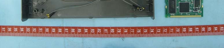
Click to zoom
Application Details
- Equipment Class
- DTS - Digital Transmission System
- Date of Grant
- Jul 18, 2005
- Application Purpose
- Original Equipment
- Date of Application
- Jul 18, 2005
- Equipment Note
- High Speed Wireless Network Adapter
- Frequency Range
- 2412.00000000 - 2462.00000000
- Company
- D-Link Corporation
- Country
- United States
Documents & Files
Document Text
Text extracted from the exhibit documents filed with the FCC. Open a document above to read the original.
Users Manual
USER’S MANUAL Model Name: Version: 1.0 Date: April/20/05 Please make sure TURN OFF your computer and remove the power cord from your PC. Open the computer case and then please insert the Wireless mini PCI Adapter. Once the Wireless mini PCI Adapter is installed , place the computer case back. Turn ON your computer. Driver Installation 1. Please select the second option and click “Next”. 2. Please click “Continue Anyway” 5. Once the installation is successful, a utility program icon will show on your desktop. To lunch the utility, just double click the icon. Federal Communication Commission Interference Statement This equipment has been tested and found to comply with the limits for a Class B digital device, pursuant to Part 15 of the FCC Rules. These limits are designed to provide reasonable protection against harmful interference in a residential installation. This equipment generates, uses and can radiate radio frequency energy and, if not installed and used in accordance with the instructions, may cause harmful interference to radio communications. However, there is no guarantee that interference will not occur in a particular installation. If this equipment does cause harmful interference to radio or television reception, which can be determined by turning the equipment off and on, the user is encouraged to try to correct the interference by one of the following measures: - Reorient or relocate the receiving antenna. - Increase the separation between the equipment and receiver. - Connect the equipment into an outlet on a circuit different from that to which the receiver is connected. - Consult the dealer or an experienced radio/TV technician for help. This device complies with Part 15 of the FCC Rules. Operation is subject to the following two conditions: (1) This device may not cause harmful interference, and (2) this device must accept any interference received, including interference that may cause undesired operation. FCC Caution: Any changes or modifications not expressly approved by the party responsible for compliance could void the user's authority to operate this equipment. IMPORTANT NOTE: FCC Radiation Exposure Statement: This equipment complies with FCC radiation exposure limits set forth for an uncontrolled environment. This equipment should be installed and operated with minimum distance 20cm between the radiator & your body. This transmitter must not be co-located or operating in conjunction with any other antenna or transmitter. To maintain compliance with FCC RF exposure compliance requirements, please avoid direct contact to the transmitting antenna during transmitting. This device is intended only for OEM integrators under the following conditions: 1) The antenna must be installed such that 20 cm is maintained between the antenna and users, and 2) The transmitter module may not be co-located with any other transmitter or antenna. 3) The module has to use the same dipole antennas, or dipole antennas with identical properties are used, AND the relative antenna spacings are maintained exactly as approved with this FCC ID. As long as 3 conditions above are met, further transmitter test will not be required. However, the OEM integrator is still responsible for testing their end-product for any additional compliance requirements required with this module installed (for example, digital device emissions, PC peripheral requirements, etc.). IMPORTANT NOTE: In the event that these conditions can not be met (for example certain laptop configurations or co-location with another transmitter), then the FCC authorization is no longer considered valid and the FCC ID can not be used on the final product. In these circumstances, the OEM integrator will be responsible for re-evaluating the end product (including the transmitter) and obtaining a separate FCC authorization. End Product Labeling This transmitter module is authorized only for use in device where the antenna may be installed such that 20 cm may be maintained between the antenna and users (for example :Access point, Wireless Router..etc.). The final end product must be labeled in a visible area with the following: “Contains TX FCC ID: KA2DI634MA2”. Manual Information That Must be Included The OEM integrator has to be aware not to provide information to the end user regarding how to install or remove this RF module in the users manual of the end product which integrate this module. The users manual for OEM integrators must include the following information in a prominent location “ IMPORTANT NOTE: To comply with FCC RF exposure compliance requirements, the antenna used for this transmitter must be installed to provide a separation distance of at least 20 cm from all persons and must not be co-located or operating in conjunction with any other antenna or transmitter. D-Link declares that the High Speed Wireless Network Adapter. (FCC ID: KA2DI634MA2) is limited in CH1~CH11 by specified firmware controlled in the USA.
External Photos
Page 1 CONSTRUCTION PHOTOS OF EUT
ID Label/Location Info
Page 1 Label location (FCC ID: KA2DI634MA2)
ID Label/Location Info
Tested To Comply With FCC Standards Made in Taiwan Rating: 3.3V FOR HOME OR OFFICE USE FCC ID: KA2DI634MA2 57mm 19mm High Speed Wireless Network Adapter Model Name: AV10 5.2mm 22.8mm
Internal Photos
Page 2 Page 3
Operational Description
D-Link Corporation FCC ID KA2DI634MA2 Theory of Operations The D-Link Corporation KA2DI634MA2 card is based on the Atheros AR2112/AR5513 chipset, which implements IEEE 802.11b, and IEEE 802.11g WLAN solutions. This all-CMOS chipset consists of the following functionality blocks: • AR2112: Radio-on-a-Chip (RoC): An all-CMOS, single-chip radio transceiver that includes a power amplifier, and integrated dual-conversion filters to convert signals from 2.4GHz to the baseband range. The AR2112 offers fully integrated transmitter, receiver, and frequency synthesizer functions; eliminating the need for external voltage controlled oscillators (VCOs) and surface acoustic wave (SAW) filters. There are two AR2112 chips on each KA2DI634MA2 card. These chips are used in two separate radio transceivers, which have outputs that are combined in the far field using phased array antennas. Refer to Theory of Operations Addendum 1 and 2 for additional details on the phased array operation. • AR5513: An all-CMOS multi-protocol MAC/Baseband processor with interfaces for Flash, SDRAM, PCI, UART, GPIO’s, and LED control. KA2DI634MA2 Block Diagram The block diagram of the KA2DI634MA2 is shown in Figure 1-1. BPF BPF 2.4GHz LNA 2.4GHz BPF AR2112 40MHz Xtal AR5513 FLASH 40MHz Clk SDRAM PCI Interface 2.4GHz OPB Front-End-Module BPF BPF 2.4GHz LNA 2.4GHz BPF 2.4GHz OPB Front-End-Module AR2112 Figure 1-1 The KA2DI634MA2 has three major sections: the digital section, the analog/RF section, and the power supplies. • The digital section consists of the Atheros AR5513 chip, SDRAM, Flash, and PCI interface. • The analog/RF section consists of two identical transceivers, each of which includes an Atheros AR2112 chip, external power booster, filters, diplexers, power detectors, external LNA, diversity switch, and antennae. • The power supplies consist of two low dropout linear regulators. AR5513 The AR5513 is the source and destination of all signals on the KA2DI634MA2 card. It contains a MAC, 180MHz MIPS R4Kc processor, SDRAM controller and Flash memory interface, PCI interface, UART interface, DACs, ADCs, General Purpose Input/Outputs, LED control outputs, and baseband circuits for transmit beamforming and multiple receive chain combining. Additional information is available on the transmit beamforming function in separate document. Flash Memory The KA2DI634MA2 card is populated with a 16M-bit serial Flash device that requires a single 3.3Vdc supply. In addition to storing operating system and application code, the Flash also stores power-on configuration for the processor and the wireless radio. Because of this, an external EEPROM is not required. PCI Interface PCI interface of the AR5513 is PCI 2.3 compatible. Power Supplies The KA2DI634MA2 card uses three voltage supply rails. 1) 3.3Vdc is supplied directly from the host device. This voltage is used to power the digital circuits of the AR2112 and AR5513 chips and to power the RF front end circuits. 2) 2.5Vdc is derived from the 3.3Vdc supply through a low drop-out linear regulator. This voltage is used to power the core of the AR2112 chips. 3) 1.8Vdc is derived from the 3.3Vdc supply through a low drop-out linear regulator. This voltage is used to power the core of the AR5513 chip. 40MHz Crystal The 40MHz crystal provides the core clock for the AR2112’s and AR5513. This crystal is attached to both AR2112’s, which internally form the reference oscillators for their respective synthesizers. The buffered 40MHz output of one of the AR2112’s then drives the 40MHz clock input of the AR5513. The maximum frequency tolerance allowed by the IEEE 802.11b/g standard is +/-20ppm. RF Front-End Overview The front-end of the KA2DI634MA2 card employs two identical 2.4GHz transceivers. Each transceiver includes an Atheros AR2112 chip, integrated front-end module, external power amplifier, external LNA, and transmit band-pass filter. The front-end module includes a diversity switch, diplexer, transmit and receive filters, and power detector. Note that the front-end module is a 2.4GHz/5GHz device; however, in this product it will only be used for 2.4GHz operation. The Atheros AR2112 does not operate in the 5GHz frequency band. The following description applies to both 2.4GHz transceivers: Tracing the transmit path, the 2.4GHz transmit signal from the AR2112 is first filtered by an LTCC bandpass filter and then boosted with an output booster (OPB). The output of the OPB is directed to an integrated front-end module. This module filters the signal, detects the transmit power level for closed loop power control, and then directs the signal to one of two diversity antennas through a diversity switch. Tracing the receive path, the 2.4GHz signal is received at the selected antenna and directed by the front-end module’s diversity switch. The signal at the output of the switch is then filtered and directed to an external low noise amplifier, which amplifies the signal, before directing it to the AR2112 for additional amplification, filtering, and down-conversion to baseband. RF Front-End Detail AR2112 The AR2112 chip is an integrated CMOS radio transceiver that supports the IEEE 802.11b, and IEEE 802.11g standards. The AR2112 supports connection to an external output booster for high performance. The transceiver core, digital logic, and VCO are powered by 2.5V. The tolerances on the 2.5V supply need to be +/-5%. The I/Os are powered by 3.3V. Matching 2.4GHz Tx output from the AR2112 is matched to external components using lumped-element matching circuits. Since there are sufficient gains in the 2.4GHz Tx front-end, a balun is not needed and a single-ended output is used. The unused output is terminated. On the receive side, a similar single-ended matching configuration is used at the 2.4GHz inputs of the AR2112. 2.4 GHz Tx Band Pass Filter (BPF) The AR2112 2.4 GHz transmit output is directed to an LTCC band-pass filter. This filter is intended to reduce spurious emissions from the AR2112 before the…
Text truncated - open the document above for the full version.
RF Exposure Info
FCC ID.: KA2DI634MA2 Report No: SA 940316L11A 1 RF EXPOSURE REPORT REPORT NO.: SA940316L11A MODEL NO.: AV10 ACCORDING: FCC Guidelines for Human Exposure IEEE C95.1 APPLICANT: D-Link Corporation ADDRESS: No.8,Li-Hsin VII Road Science Based Industrial Park Hsin-Chu,Taiwan ISSUED BY: Advance Data Technology Corporation LAB LOCATION: 47 14th Lin, Chiapau Tsun, Linko, Taipei, Taiwan, R.O.C. TEST LOCATION: No. 19, Hwa Ya 2nd Rd., Wen Hwa Tsuen, Kwei Shan Hsiang, Taoyuan Hsien 333, Taiwan, R.O.C. FCC ID.: KA2DI634MA2 Report No: SA 940316L11A 2 RF Exposure Measurement (Mobile Device) 1. Introduction In this document, we try to prove the safety of radiation harmfulness to the human body for our product. The limit for Maximum Permissible Exposure (MPE) specified in FCC 1.1310 is followed. The Gain of the antenna used in this product is measured in a Fully Anechoic Chamber (FAC) calibrated for antenna measurement in ADT, and also the maximum total power input to the antenna is measured. Through the Friis transmission formula and the maximum gain of the antenna, we can calculate the distance, away from the product, where the limit of MPE is reached. Although the Friis transmission formula is a far field assumption, the calculated result of that is an over-prediction for near field power density. We will take that as the worst case to specify the safety range. 2. RF Exposure Limit According to FCC 1.1310: The criteria listed in the following table shall be used to evaluate the environmental impact of human exposure to radio-frequency (RF) radiation as specified in 1.1307(b) LIMITS FOR MAXIMUM PERMISSIBLE EXPOSURE (MPE) Frequency Range (MHz) Electric Field Strength (V/m) Magnetic Field Strength (A/m) Power Density (mW/cm 2 ) Average Time (minutes) (A)Limits For Occupational / Control Exposures 300-1500......F/3006 1500-100,000......56 (B)Limits For General Population / Uncontrolled Exposure 300-1500......F/15006 1500-100,000......1.030 F = Frequency in MHz FCC ID.: KA2DI634MA2 Report No: SA 940316L11A 3 3. Friis Formula Friis transmission formula : Pd = (Pout*G) / (4*pi*r 2 ) where Pd = power density in mW/cm 2 Pout = output power to antenna in mW G = gain of antenna in linear scale Pi = 3.1416 R = distance between observation point and center of the radiator in cm If we know the maximum Gain of the antenna and the total power input to the antenna, through the calculation, we will know the MPE value at distance r. Ref. : David K. Cheng, Field and Wave Electromagnetics, Second Edition, Page 640, Eq. (11-133). 4 EUT Operating condition The software provided by Manufacturer enabled the EUT to transmit and receive data at lowest, middle and highest channel individually. 5. Classification This modular is specified to be installed in access point or router which is connected with host through wire. So it is easy to be re-located in the place where at least 20cm far away from the body of the user. Warning statement to the user for keeping at least 20cm or more separation distance with the antenna should be included in users manual. So, this device is classified as Mobile Device. FCC ID.: KA2DI634MA2 Report No: SA 940316L11A 4 6 Test Results 6.1 Antenna Gain The maximum Gain measured in Fully Anechoic Chamber is 2.319dBi or 1.706(numeric) 6.2 Output Power Into Antenna & RF Exposure value at distance 20cm: Signal Chain 802.11b DSSS modulation Channel Channel Frequency (MHz) Output Power to Antenna (mW) Power Density (mW/cm 2 ) Limit of Power Density (mW/cm 2 ) 1241250.6990.0171.0 6243736.5330.0221.0 11246250.3500.0171.0 802.11g OFDM modulation Channel Channel Frequency (MHz) Output Power to Antenna (mW) Power Density (mW/cm 2 ) Limit of Power Density (mW/cm 2 ) 1241244.8750.0151.0 6243763.8260.0221.0 11246245.1860.0151.0 802.11g Turbo OFDM modulation Channel Channel Frequency (MHz) Output Power to Antenna (mW) Power Density (mW/cm 2 ) Limit of Power Density (mW/cm 2 ) 6243763.6800.0221.0 Dual Chain PEAK POWER OUTPUT (mW) PEAK POWER OUTPUT (dBm) CHANNEL CHANNEL FREQUENCY (MHz) CHAIN 0 CHAIN 1 CHAIN 0 CHAIN 1 TOTAL PEAK POWER (mW) TOTAL PEAK POWER (dBm) POWER DENSITY (mW/CM2)) LIMIT OF POWER DENSITY (mW/CM2) 1241220.13720.04513.0413.0240.18216.040.0141.0 2241763.38763.82618.0218.05127.21321.050.0431.0 3242264.12163.38718.0718.02127.50821.060.0431.0 6243764.71463.53318.1118.03128.24721.080.0441.0 9245263.68063.97318.0418.06127.65321.060.0431.0 10245763.82664.41718.0518.09128.24321.080.0441.0 11246220.18420.46413.0513.1140.64816.090.0141.0 FCC ID.: KA2DI634MA2 Report No: SA 940316L11A 5 802.11g Turbo OFDM modulation PEAK POWER OUTPUT (mW) PEAK POWER OUTPUT (dBm) CHANNEL CHANNEL FREQUENCY (MHz) CHAIN 0 CHAIN 1 CHAIN 0 CHAIN 1 TOTAL PEAK POWER (mW) TOTAL PEAK POWER (dBm) POWER DENSITY (mW/CM2)) LIMIT OF POWER DENSITY (mW/CM2) 6243732.50931.84215.1215.0364.35118.090.0221.0
Test Report
FCC ID: KA2DI634MA2 Report No.: RF940316L11A1Report Format Version 2.0.1 Reference No.: 940627L05 FCC TEST REPORT REPORT NO.: RF940316L11A MODEL NO.: AV10 RECEIVED: NA TESTED: Mar. 15 ~ Mar. 22, 2005 ISSUED: Jun. 28, 2005 APPLICANT: D-Link Corporation ADDRESS: No.8,Li-Hsin VII Road Science Based Industrial Park Hsin-Chu,Taiwan ISSUED BY: Advance Data Technology Corporation LAB ADDRESS: 47 14 th Lin, Chiapau Tsun, Linko, Taipei, Taiwan, R.O.C. TEST LOCATION: No. 19, Hwa Ya 2 nd Rd., Kueishan, Taoyuan, Taiwan, R.O.C. This test report consists of 174 pages in total. It may be duplicated completely for legal use with the approval of the applicant. It should not be reproduced except in full, without the written approval of our laboratory. The client should not use it to claim product endorsement by CNLA, A2LA or any government agencies. The test results in the report only apply to the tested sample. 0528 ILAC MRA No. 2177-01 FCC ID: KA2DI634MA2 Report No.: RF940316L11A2Report Format Version 2.0.1 Reference No.: 940627L05 Table of Contents 1CERTIFICATION ..........................................................................................................6 2SUMMARY OF TEST RESULTS .................................................................................7 2.1MEASUREMENT UNCERTAINTY ...............................................................................7 3GENERAL INFORMATION ..........................................................................................8 3.1GENERAL DESCRIPTION OF EUT.............................................................................8 3.2DESCRIPTION OF TEST MODES.............................................................................10 3.2.1 CONFIGURATION OF SYSTEM UNDER TEST........................................................10 3.2.2 TEST MODE APPLICABILITY AND TESTED CHANNEL DETAIL ............................11 3.3GENERAL DESCRIPTION OF APPLIED STANDARDS............................................15 3.4DESCRIPTION OF SUPPORT UNITS .......................................................................15 4TEST TYPES AND RESULTS (FOR SINGLE CHAIN (TX)) ......................................16 4.1CONDUCTED EMISSION MEASUREMENT .............................................................16 4.1.1 LIMITS OF CONDUCTED EMISSION MEASUREMENT...........................................16 4.1.2 TEST INSTRUMENTS ...............................................................................................16 4.1.3 TEST PROCEDURES ................................................................................................17 4.1.4 DEVIATION FROM TEST STANDARD......................................................................17 4.1.5 TEST SETUP .............................................................................................................18 4.1.6 EUT OPERATING CONDITIONS...............................................................................18 4.1.7 TEST RESULTS .........................................................................................................19 4.2RADIATED EMISSION MEASUREMENT ..................................................................31 4.2.1 LIMITS OF RADIATED EMISSION MEASUREMENT ...............................................31 4.2.2 TEST INSTRUMENTS ...............................................................................................32 4.2.3 TEST PROCEDURES ................................................................................................33 4.2.4 DEVIATION FROM TEST STANDARD......................................................................33 4.2.5 TEST SETUP .............................................................................................................34 4.2.6 EUT OPERATING CONDITIONS...............................................................................34 4.2.7 TEST RESULTS .........................................................................................................35 4.36dB BANDWIDTH MEASUREMENT .........................................................................59 4.3.1 LIMITS OF 6dB BANDWIDTH MEASUREMENT .......................................................59 4.3.2 TEST INSTRUMENTS ...............................................................................................59 4.3.3 TEST PROCEDURE ..................................................................................................60 4.3.4 DEVIATION FROM TEST STANDARD......................................................................60 4.3.5 TEST SETUP .............................................................................................................60 4.3.6 EUT OPERATING CONDITIONS...............................................................................60 FCC ID: KA2DI634MA2 Report No.: RF940316L11A3Report Format Version 2.0.1 Reference No.: 940627L05 4.3.7 TEST RESULTS .........................................................................................................61 4.4MAXIMUM PEAK OUTPUT POWER .........................................................................69 4.4.1 LIMITS OF MAXIMUM PEAK OUTPUT POWER MEASUREMENT..........................69 4.4.2 TEST INSTRUMENTS ...............................................................................................69 4.4.3 TEST PROCEDURES ................................................................................................70 4.4.4 DEVIATION FROM TEST STANDARD......................................................................70 4.4.5 TEST SETUP .............................................................................................................70 4.4.6 EUT OPERATING CONDITIONS...............................................................................70 4.4.7 TEST RESULTS .........................................................................................................71 4.5POWER SPECTRAL DENSITY MEASUREMENT...........................…
Text truncated - open the document above for the full version.
Test Report
FCC ID: KA2DI634MA2 Report No.: RF940316L11A99Report Format Version 2.0.1 Reference No.: 940627L05 5 TEST TYPES AND RESULTS (For Dual Chain (TX)) 5.1 CONDUCTED EMISSION MEASUREMENT 5.1.1 LIMITS OF CONDUCTED EMISSION MEASUREMENT FREQUENCY OF EMISSION (MHz)CONDUCTED LIMIT (dBμV) Quasi-peakAverage 0.15-0.5 0.5-5 5-30 66 to 56 56 60 56 to 46 46 50 NOTE:1. The lower limit shall apply at the transition frequencies. 2. The limit decreases in line with the logarithm of the frequency in the range of 0.15 to 0.50 MHz. 3. All emanations from a class A/B digital device or system, including any network of conductors and apparatus connected thereto, shall not exceed the level of field strengths specified above. 5.1.2 TEST INSTRUMENTS DESCRIPTION & MANUFACTURERMODEL NO.SERIAL NO.CALIBRATED UNTIL Test Receiver ROHDE & SCHWARZ ESCS30100291Nov. 16, 2005 RF signal cable Woken 5D-FBCable-HYC01-01Jan. 09, 2006 LISN ROHDE & SCHWARZ ESH3-Z5100312Feb. 15, 2006 LISN ROHDE & SCHWARZ ESH2-Z5100104Feb. 15, 2006 Software ADT ADT_Cond_V3NANA NOTE: 1. The calibration interval of the above test instruments is 12 months and the calibrations are traceable to NML/ROC and NIST/USA. 2. The test was performed in HwaYa Shielded Room 1. 3. The VCCI Site Registration No. is C-2040. FCC ID: KA2DI634MA2 Report No.: RF940316L11A100Report Format Version 2.0.1 Reference No.: 940627L05 5.1.3 TEST PROCEDURES d. The EUT was placed 0.4 meters from the conducting wall of the shielded room with EUT being connected to the power mains through a line impedance stabilization network (LISN). Other support units were connected to the power mains through another LISN. The two LISNs provide 50 ohm/ 50uH of coupling impedance for the measuring instrument. e. Both lines of the power mains connected to the EUT were checked for maximum conducted interference. f. The frequency range from 150kHz to 30MHz was searched. Emission levels under Limit - 20dB was not recorded. 5.1.4 DEVIATION FROM TEST STANDARD No deviation FCC ID: KA2DI634MA2 Report No.: RF940316L11A101Report Format Version 2.0.1 Reference No.: 940627L05 5.1.5 TEST SETUP For the actual test configuration, please refer to the related item – Photographs of the Test Configuration. 5.1.6 EUT OPERATING CONDITIONS a. Connected the EUT with extended mini PCI card to a notebook system placed on a testing table. b. The notebook system ran a test program (provided by manufacturer) to enable EUT under transmission/receiving condition continuously at specific channel frequency. c. The notebook system show “H” messages on its screen. d. Repeated item c. FCC ID: KA2DI634MA2 Report No.: RF940316L11A102Report Format Version 2.0.1 Reference No.: 940627L05 5.1.7 TEST RESULTS Conducted Worst Case Data 802.11g OFDM modulation EUT High Speed Wireless Network Adapter MEASUREMENT DETAIL MODEL AV10 PHASE Line 1 CHANNEL Channel 1 6dB BANDWIDTH 9 kHz MODULATION TYPE BPSK ENVIRONMENTAL CONDITIONS 20deg. C, 74%RH, 991hPa TRANSFER RATE 6Mbps INPUT POWER (SYSTEM) 120Vac, 60 Hz TEST CONFIGURE MODE 2TEST MODE Dual chain TESTED BY Scott Yang Freq.Corr.Reading Value Emission Level LimitMargin NoFactor[dB (uV)][dB (uV)][dB (uV)](dB) [MHz](dB)Q.P.AV.Q.P.AV.Q.P.AV.Q.P.AV. 10.1700.1045.52-45.62-64.9854.98-19.36- 20.2050.1146.31-46.42-63.4253.42-17.00- 30.3100.1133.57-33.68-59.9749.97-26.28- 42.0390.2128.69-28.90-56.0046.00-27.10- 59.8590.4233.67-34.09-60.0050.00-25.91- 616.8790.7528.96-29.71-60.0050.00-30.29- *(The test data is in accordance with ADT Report No.: RF940316L11.) REMARKS: 1. Q.P. and AV. are abbreviations of quasi-peak and average individually. 2. "-": The Quasi-peak reading value also meets average limit and measurement with the average detector is unnecessary. 3. The emission levels of other frequencies were very low against the limit. 4. Margin value = Emission level - Limit value 5. Correction factor = Insertion loss + Cable loss 6. Emission Level = Correction Factor + Reading Value. FCC ID: KA2DI634MA2 Report No.: RF940316L11A103Report Format Version 2.0.1 Reference No.: 940627L05 EUT High Speed Wireless Network Adapter MEASUREMENT DETAIL MODEL AV10 PHASE Line 2 CHANNEL Channel 1 6dB BANDWIDTH 9 kHz MODULATION TYPE BPSK ENVIRONMENTAL CONDITIONS 20deg. C, 74%RH, 991hPa TRANSFER RATE 6Mbps INPUT POWER (SYSTEM) 120Vac, 60 Hz TEST CONFIGURE MODE 2TEST MODE Dual chain TESTED BY Scott Yang Freq.Corr.Reading Value Emission Level LimitMargin NoFactor[dB (uV)][dB (uV)][dB (uV)](dB) [MHz](dB)Q.P.AV.Q.P.AV.Q.P.AV.Q.P.AV. 10.1700.1046.01-46.11-64.9854.98-18.88- 20.2050.1046.41-46.51-63.4253.42-16.91- 30.6320.1330.22-30.35-56.0046.00-25.65- 42.0220.2128.04-28.25-56.0046.00-27.75- 510.0470.4032.90-33.30-60.0050.00-26.70- 614.7850.4931.01-31.50-60.0050.00-28.50- *(The test data is in accordance with ADT Report No.: RF940316L11.) REMARKS: 1. Q.P. and AV. are abbreviations of quasi-peak and average individually. 2. "-": The Quasi-peak reading value also meets average limit and measurement with the average detector is unnecessary. 3. The emission levels of other frequencies were very low against the limit. 4. Margin value = Emission level - Limit value 5. Correction factor = Insertion loss + Cable loss 6. Emission Level = Correction Factor + Reading Value. FCC ID: KA2DI634MA2 Report No.: RF940316L11A104Report Format Version 2.0.1 Reference No.: 940627L05 EUT High Speed Wireless Network Adapter MEASUREMENT DETAIL MODEL AV10 PHASE Line 1 CHANNEL Channel 6 6dB BANDWIDTH 9 kHz MODULATION TYPE BPSK ENVIRONMENTAL CONDITIONS 20deg. C, 74%RH, 991hPa TRANSFER RATE 6Mbps INPUT POWER (SYSTEM) 120Vac, 60 Hz TEST CONFIGURE MODE 2TEST MODE Dual chain TESTED BY Scott Yang Freq.Corr.Reading Value Emission Level LimitMargin NoFactor[dB (uV)][dB (uV)][dB (uV)](dB) [MHz](dB)Q.P.AV.Q.P.AV.Q.P.AV.Q.P.AV. 10.1730.1046.37-46.47-64.7954.79-18.32- 20.2090.1145.57-45.68-63.2653.26-17.58- 30.3140.1132.74-32.85-59.8649.86-27.01- 41.9530.2128.79-29.00-56.0046.00-27.00- 510.3240.4333.26-33.69-60.0050.00-26.31- 616.0510.7029.55-30.25-60.0050.00-29.75- *(The t…
Text truncated - open the document above for the full version.
Test Report
FCC ID: KA2DI634MA2 ADT No. 940316L11A Modular Approval Request Letter Advance Data Technology 07July 2004 Dear Application Examiner, D-Link Corporation, It’s High Speed Wireless Network Adapter, FCC ID: KA2DI634MA2, would like to have your authorization as a limited modular approval specific to the mobile device such as Access Point. The requirements of Public Notice DA00-1407 have been met and shown on the following statements. 1. “The modular transmitter must have its own RF shielding.”: The radio portion of this module has been shielded, please see exhibition External Photo. 2. “The modular transmitter must have buffered modulation/data inputs.” The EUT has buffered data inputs, it is integrated in chip AR5513A. 3. “The modular transmitter must have its own power supply regulation.” The chips IF converter and RF/IF converter which will influence the frequency radiation, have to be 1.80Vdc powered. The mini-pci interface provides 3.3Vdc, so there are regulators in front of these chips, the part number of this regulator is VR2. 4. “The modular transmitter must comply with the antenna requirements of section 15.203 and 15.204(C).” The EUT meets the FCC antenna requirements. The spurious emission, unique antenna connector and photo of antennas are shown in the test report. 5. “The modular transmitter must be tested in a stand-alone configuration” The EUT was tested in a stand-alone configuration via a PCMCIA to mini-PCI extender. Please see section Photographs of Test Configuration in the test report, the EUT was plugged in this extender. 6. “The modular transmitter must be labeled with its own FCC ID number.” Please see exhibition Label Sample for the FCC ID of this module. And also in the exhibition Users Manual, there are instructions give to the OEM on how to label the end product. FCC ID: KA2DI634MA2 ADT No. 940316L11A 7. “The modular transmitter must comply with any specific rule or oper…
Text truncated - open the document above for the full version.
Contact Information
Applicant
Brett Adair(General Counsel)
Technical Contact
Advance Data Technology CorporatiojnCody Chang
[email protected]883-3-3183232
No. 19, Hwa Ya 2nd Rd., Kwei Shan Hsiang · Taoyuan Hsien · Taiwan
Non-Technical Contact
Advance Data Technology CorporationStephanie Hung
[email protected]886-3-3183232
Test Firm
Bureau Veritas CPS (H.K.) Ltd. Taoyuan BranchRichard Chen
Technical Specifications
| # | Rule Parts | Frequency Range | Power Output |
|---|---|---|---|
| 1 | 15C | 2.41 GHz - 2.46 GHz | 128.00 mW |
Other Applications from D-Link Corporation
KA2CS6012A1
Jul 07, 20262K Fixed Indoor Cloud Camera, 2K Fixed Indoor Wi-Fi Camera
Equipment Class
DTS - Digital Transmission SystemKA2AE65UA1
Mar 02, 2026Wi-Fi 7 BE6500 USB 3.0 Dongle
Equipment Class
NII - Unlicensed National Information Infrastructure TXKA2APE9560A1
Nov 17, 2025BE9500 Celling mount Access Point
Equipment Class
6ID - 15E 6 GHz Low Power Indoor Access PointKA2AX9UA1
Dec 04, 2024AX900 Wi-Fi 6 USB Adapter, Wi-Fi 6 AX900 USB 2.0 Dongle
Equipment Class
DSS - Part 15 Spread Spectrum TransmitterKA2AC13UA1
Dec 04, 2024AC1300 Wi-Fi 5 USB Adapter, Wi-Fi 5 AC1300 USB 2.0 Dongle
Equipment Class
DTS - Digital Transmission System