KOBFR04P150Automotive Receiver
Lear Corporation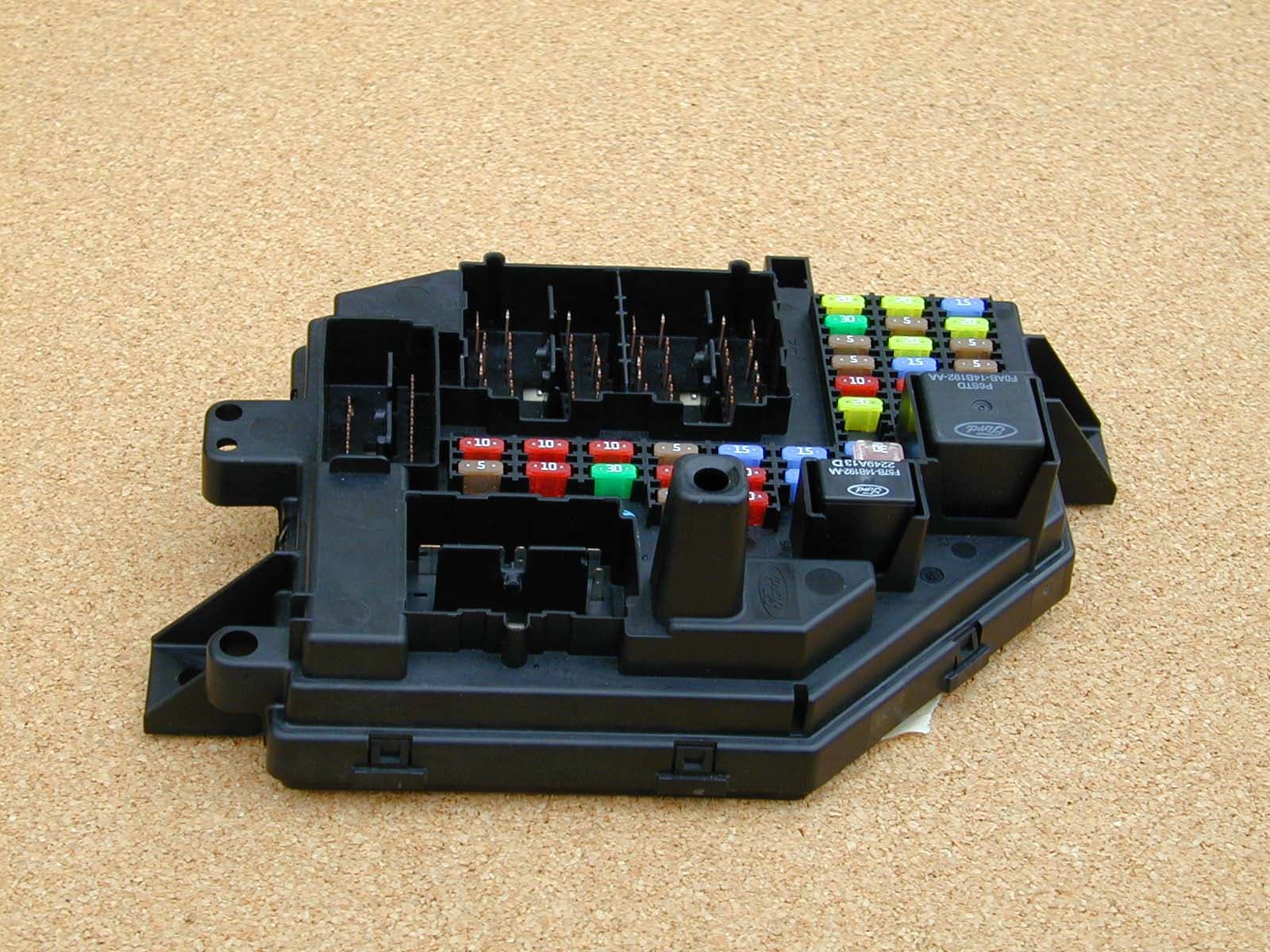
Click to zoom
Application Details
- Equipment Class
- CYY - Communications Receiver used w/Pt 15 Transmitter
- Date of Grant
- Jan 05, 2003
- Application Purpose
- Original Equipment
- Date of Application
- Jan 05, 2003
- Equipment Note
- Automotive Receiver
- Frequency Range
- 315.00000000 - 315.00000000
- Company
- Lear Corporation
- Country
- United States
Documents & Files
Document Text
Text extracted from the exhibit documents filed with the FCC. Open a document above to read the original.
Users Manual
Re: Certification for Lear MY04P150 Receiver Model: MY04P150 FCC ID: KOBFR04P150 IC: 3521A- FR04P150 USER'S MANUAL INFORMATION (PRELIMINARY) The User's Manual is in preparation. The following material will be contained in the manual: FCC ID: KOBFR04P150 IC: 3521A- FR04P150 This device complies with Part 15 of the FCC Rules and with RSS-210 of Industry Canada. Operation is subject to the following two conditions: (1) This device may not cause harmful interference, and (2) This device must accept any interference received, including interference that may cause undesired operation. WARNING: Changes or modifications not expressively approved by the party responsible for compliance could void the user's authority to operate the equipment. The term “IC:” before the radio certification number only signifies that Industry Canada technical specifications were met.
Block Diagram
ENGINEER Craig Elder Document I/O Functional Block Diagram HW130 and HW140 DATE 4/24/2002 5200 Auto Club Drive Dearborn, Michigan 48126-9982 313/593-9000 APPROVED BY Project P150 MY2004 SJB Page 1 of 1 VERSION 1.0 MC9S12D64VPV Microprocessor 105degC 112pin LQFP Internal PLL Ram: 512Bytes of 4KB EEPROM: 512Bytes of 1KB Flash: 30KB of 64KB I/O Totals DInputs: 24 (2+7+14+1) Doutputs: 11 (1+4+1+4+1) Key IRQs:3 (1+1+1) IOC: 2 (1+1) A/D: 6 (1+1+3+1) SCI Ports:1 SPI Ports: 1 5V Voltage Regulator 5V x 50mA 1 A/D Feedback for overvoltage 7 Active High Digital Inputs Isink < 0.13mA/ea. (Window_up_cmd, Window_down_cmd, Ign_run/start, Ign_run/acc, High_beam_sense, Dome_lamp_sense, Park_Lamp_sense) 14 Active Low Digital Inputs Iwett < 28mA/ea. (wiper_motorstat, BOO_sw, dd_ajar_sw, pd_ajar_sw, telematics_lock, telematics_unlock, park_brake_sw, door_lock_sw, door_unlock_sw, wiper_w/h/ c/b/a) One Touch Down High Low Current Sense coverted to Voltage 1 A/D 1 DIO 2 RF Inputs 1 Key Interupt signals incoming RF message (Not Used) 1 Input Capture used to decode the signal 1 Sensor input 1 Input Capture used to count VSS 8000PPM pulse train (Not Used) 4Mhz +/- 0.5% Ceramic Resonator PLL @ 16MHz Communication Bus (1 SCI Port) Protocol: ISO-9141 Bit Width: 96uS Tolerance: 2% Fog Interupt High Side Load (1 digital output, 1 digital input) 16 Low Current Loads using 2 Octal Low Side Drivers (1 SPI Port, 4 Digital Outputs for CSB', SFPD') 12 Relay Coils (wiper_speed_relay, wiper_runpark_relay, wiper_wash_relay, spare , battery_saver_relay, 1touchdown_relay, horn_relay, park_lamp_relay, all_lock_relay, driver_unlock_relay, pass_unlock_relay, Interior_Lamp_Relay) 4 Lamp Indicators (TPMS_lamp1 -4) Daytime Running Lamps (1 DIO/PWM output, 1Key Interupt, 1A/D feedback) PWM Duty Cyle: 72-90% PWM Frequency: 100Hz Sleep Timers Keywakeup IRQ every 33-39mS (1 DIO required to charge/enable/ disable, 1 Key Interupt required to wake MCU from stop mode, 1 DIO for RKE strobe) Notes: Active High Sink Current = (18.83V - 5.6V)/100K = 0.13mA assuming internal clamp diodes. Active Low Wetting Current = (18.83V)/680 = 28mA current provides by a switched battery supply. 4 Switched Supplys Vccsw: 15mA Vbatsw1: 150mA Vbatsw2: 225mA Vbatsw3: 50mA 4Digital Outputs, 3 A/D feedbacks on vbatsw1&2&3 LCB is using 49 of 51 available Long Pin Connections Refer to the P150 HITS specification for MCU pinout - LNA Low Noise Amplifier Mixer 10.7MHz IF Filter Multi-Stage IF Amp PLL Synthesiser Crystal Oscillator Matching Networks Carrier Freq. Pre- Selector Antenna Data Slicer Envelope Detector Super-Heterodyne Receiver Block Diagram Demodulated Data BlockPurposeExample AntennaCapture radiated RF energy and couple energy into receiver front end. PCB trace, Rigid wire, External wire Frequency Pre-SelectorSuppress image frequency and out of band jamming sources. SAW (Surface Acoustic Wave) Filter. Matching NetworksTransfer maximum energy between the different stages LC network, Integrated filter components. Low Noise AmplifierProvide RF signal amplification with minimum noise. Cascode Amplifier. MixerConvert the input frequency (RF) to an intermediate frequency (IF). Double Balanced Mixer IF FilterSet System BandwidthCeramic, LC networks. IF Cascaded AmplifiersProvide IF signal amplification Cascode Amplifiers Envelope DetectorConvert IF frequency to DC voltage levels. Diode detector with low pass filter. Data SlicerCondition demodulated data to logic levels for microprocessor decoding. Operational Amplifiers using RC timing components
Cover Letter(s)
Re: Certification for Lear MY04P150 Receiver Model: MY04P150 FCC ID: KOBFR04P150 IC: 3521A- FR04P150 REQUEST FOR CONFIDENTIALITY Pursuant to 47 CRF 0.459, Lear requests that a part of the subject application be held confidential. This comprises Exhibits (5) Schematics (10) Parts List (Part of Exhibit only) Lear has spent substantial effort in developing this product and it is one of the first of its kind in industry. Having the subject information easily available to "competition" would negate the advantage they have achieved by developing this product. Not protecting the details of the design will result in financial hardship. If there are any questions regarding this request, please contact me at the above address or call 734-483-4211, fax 734-647-2106 or e-mail [email protected]. Sincerely, Valdis V. Liepa Research Scientist University of Michigan January 4, 2003 Re: Certification for Lear MY04P150 Receiver Model: MY04P150 FCC ID: KOBFR04P150 IC: 3521A- FR04P150 STATEMENT OF MODIFICATIONS There were no modifications made to the DUT by this test laboratory. (Also see Section 3.1 of the attached Test Report). _____________________ Valdis V. Liepa Research Scientist Re: Certification for Lear MY04P150 Receiver Model: MY04P150 FCC ID: KOBFR04P150 IC: 3521A- FR04P150 GENERAL PRODUCT INFORMATION The device, for which certification is pursued, has been designed by: Lear Corporation 3521A- FR04P150 5200 Auto Club Drive Dearborn, MI 48126 Gerard Grabowski Tel: 313-593-9604 Fax: 313-240-3832 It will be manufactured by: Lear Corporation 5200 Auto Club Drive Dearborn, MI 48126 Gerard Grabowski Tel: 313-593-9604 Fax: 313-240-3832 Canadian Contact: Ford Motor Company of Canada Limited The Canadian Road P.O. Box 2000 Oakville, Ontario, Canada L6J 5E4 HR Personell 800-565-3673 905-845-4642 Re: Certification for Lear MY04P150 Receiver Model: MY04P150 FCC ID: KOBFR04P150 IC: 3521A- FR04P150 POWER OF ATTORNEY A letter granting Valdis V. Liepa the Power of Attorney is on file and can be provided when so requested.
Cover Letter(s)
RE: Lear Corporation FCC ID: KOBFR04P150 This is in response to the comments made on the above application. 1) The 731 form shows that this application is for a receiver. However, from the operational and internal photographs this is not easily determined. Please provide a photograph that shows/labels the portion of the device that is the RX and also the antenna for the RX. Additional internal photographs have been uploaded demonstrating the RX circuitry and the antenna. 2) The block diagram should show the frequencies of the oscillator within the RX (CFR 2.1033(a)(5)). Please provide an updated version that includes this information. A revised Block Diagram has been uploaded. 3) The label appears to show the FCC ID as KOBFR04P150, while the label appears as KOBFRO4P150. Please confirm which FCC ID Number is correct using a ‘0’ or ‘O’. This is a simple typo, the FCC ID is KOBFR04P15 and an revised ID label has been uploaded. 4) Please provide a photograph or drawing that shows the placement of the label on the device. See revised ID Label & Location Exhibit. 5) The FCC ID given in the test report in section 3 does not match the FCC given in this application. The FCC ID should now match that of the ID label, and all other references. 6) The frequency of the signal injected in section 5.1 is not given or appears to be left out. Section 5.1 shows 315 MHz. In either case, injection is required only for superregenerative and not superheterodyne receivers.
Cover Letter(s)
American Telecommunications Certification Body Inc. 6731 Whittier Ave, McLean, VA 22101 January 5, 2003 RE: Lear Corporation FCC ID: KOBFR04P150 After a review of the submitted information, I have a few comments on the above referenced Application. 1) The 731 form shows that this application is for a receiver. However, from the operational and internal photographs this is not easily determined. Please provide a photograph that shows/labels the portion of the device that is the RX and also the antenna for the RX. 2) The block diagram should show the frequencies of the oscillator within the RX (CFR 2.1033(a)(5)). Please provide an updated version that includes this information. 3) The label appears to show the FCC ID as KOBFR04P150, while the label appears as KOBFRO4P150. Please confirm which FCC ID Number is correct using a ‘0’ or ‘O’. 4) Please provide a photograph or drawing that shows the placement of the label on the device. 5) The FCC ID given in the test report in section 3 does not match the FCC given in this application. 6) The frequency of the signal injected in section 5.1 is not given or appears to be left out. Timothy R. Johnson Examining Engineer mailto: [email protected] The items indicated above must be submitted before processing can continue on the above referenced application. Failure to provide the requested information may result in application termination. Correspondence should be considered part of the permanent submission and may be viewed from the Internet after a Grant of Equipment Authorization is issued. Please do not respond to this correspondence using the email reply button. In order for your response to be processed expeditiously, you must submit your documents through the AmericanTCB.com website. Also, please note that partial responses increase processing time and should not be submitted. Any questions about the content of this correspondence should be directed to the sender.
ID Label/Location Info
FCC ID: KOBFR04P150 IC: 3521A-FR04P150 THIS DEVICE COMPLIES WITH PART 15 OF THE FCC RULES AND WITH RSS-210 OF INDUSTRY CANADA. OPERATION IS SUBJECT TO THE FOLLOWING TWO CONDITIONS: (1) THIS DEVICE MAY NOT CAUSE HARMFUL INTERFERENCE. AND (2) THIS DEVICE MUST ACCEPT ANY INTERFERENCE RECEIVED, INCLUDING UNDESIRED OPERATION
Operational Description
1.1Product Family Description The SJB described herein forms the foundation of the Body Electrical/Electronic Subsystem. The SJB combines the Generic Electronic s Module (GEM) and Junction Box (JB) into a single entity for the 2004 Ranger. The SJB is an electronic assembly consisting of two separate PCBs – one for high current loads (HCB) and the other for the low current electronics (LCB). The HCB is single sided with components populated on one side while the LCB is doubled sided with components populated on both sides. The SJB monitors and controls vehicle functions as described in Table 1-2. All relays are located on the HCB or external to the SJB in the Power Distribution Center (PDC).
Test Report
10 DUT on OATS Close-up on the DUT on OATS
Test Setup Photos
10 DUT on OATS Close-up on the DUT on OATS
Contact Information
Applicant
Kristof von Czarnowski(RF Engineer)
Technical Contact
University of Michigan/EECSValdis V Liepa
[email protected]734-483-4211
1301 Beal Ave. · Ann Arbor, Michigan · United States
Non-Technical Contact
University of Michigan/EECSValdis V Liepa
[email protected]734-483-4211
Test Firm
University of MichiganValdis Liepa
Technical Specifications
| # | Rule Parts | Frequency Range | Power Output |
|---|---|---|---|
| 1 | 15B | 315 MHz - 315 MHz | - |
Other Applications from Lear Corporation
KOBJXF23B
Jul 20, 2026RKE Transmitter with UWB
Equipment Class
DSC - Part 15 Security/Remote Control Transmitter
KOBJXF23A
Sep 26, 2023RKE Transmitter with UWB
Equipment Class
DSC - Part 15 Security/Remote Control Transmitter
KOBHT13BTPM
Oct 15, 2012Security/Remote Control Transmitter
Equipment Class
DSC - Part 15 Security/Remote Control TransmitterKOBATA12A
Jun 20, 2012Remote keyless entry / Remote start
Equipment Class
DSC - Part 15 Security/Remote Control Transmitter
KOBGTE12A
Apr 20, 2012Car2U System TX
Equipment Class
DSC - Part 15 Security/Remote Control Transmitter