L9N-7880UHF TRANSCEIVER
AES Corporation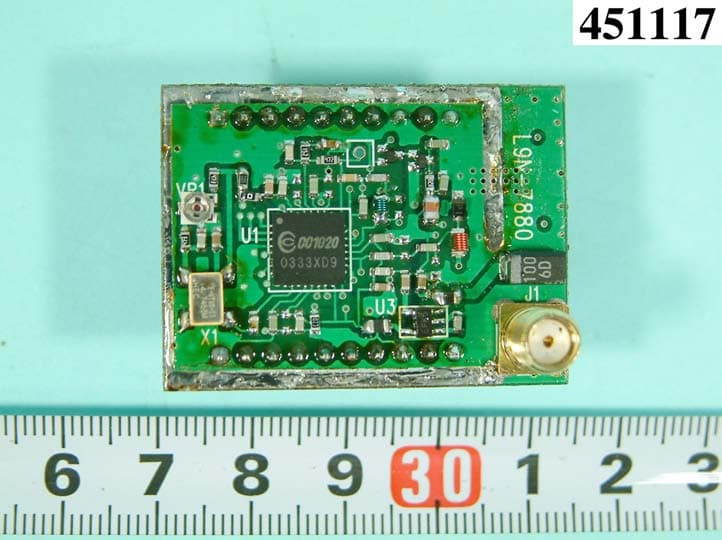
Click to zoom
Application Details
- Equipment Class
- LMS - Part 90 Location & Monitoring Transmitter
- Date of Grant
- Jul 19, 2004
- Application Purpose
- Original Equipment
- Date of Application
- Jul 19, 2004
- Equipment Note
- UHF TRANSCEIVER
- Frequency Range
- 450.00000000 - 470.00000000
- Company
- AES Corporation
- Country
- United States
Documents & Files
Document Text
Text extracted from the exhibit documents filed with the FCC. Open a document above to read the original.
Users Manual
L9N-7880 UHF DATA TRANSCEIVERS . PLL SYNTHESIZED 1. SPECIFICATION GENERAL SPECIFICATIONS POWER SOURCE .............................................+5VD.C. TEMPERATURE RANGE STORAGE ..............................................80 maximum -40 min. 25 nominal OPERATING ...........................................60 maximum -20 min. ANTENNA IMPEDANCE .......................................50 FREQUENCY CONTROL ..........................................PLL SYNTHESISER FREQUENCIES OF OPERATION .............................402MHZ-470MHZ FREQUENCY TOLERANCE AND STABILITY ............±2.5PPM HIGH HUMIDITY .................................................90 CHANNEL CAPABILITY ........................................1 NOMINAL DIMENSIONS ........................................40(L)X30(W)X20(H) WEIGHT ................................................................16g RADIO DATA TRANSCEIVER NOMINAL PERFORMANCE PERFORMANCE SPECIFICATIONS ..............................FCC part 90 RF OUTPUT POWER ............................................0.7w MODULATION TYPE ..............................................FM INTERMEDIATE FREQUENICES ...............................307.2 khz CHANNEL SPACING ...............................................25KHZ TRANSMIT ATTACK TIME ..............................25 mS CURRENT CONSUMPTION TRANSMIT [email protected] RECEIVE ......................................2.5mA PAGE2 14.7456 MHz VCTCXO An external clock signal from VCTCXO X1 is connect to CC1020 XOSC_Q1 , This VCTCXO is only 5x3.2x1.4(H) mm, and is manufactured with a ceramic base and metal lid to assure very good aging characteristics and reliability. This device offers an in ±2.5PPM over -30 to +75 Celsius. The VR1 is used to adjust the frequency is as close as possible to the exact required transmit frequency. Ideally it should be within 100 Hz at room temperature. PA module The U2 is a power amplifier IC as the final RF amplifier in the 400MHz to 480MHz band. Low pass filter The amplifier RF signal is through the harmonic low pass filter, comprising L63 to L65 and C62-C66 and then to the antenna connector J1. Antenna switch When transmitting, the diode D61 and D60 are forward biased, allowing the RF to pass to the antenna. D60 is shorted to ground which makes L61 look open circuit (1/4 wave tuned stub ). This prevents the TX signal from passing to the receiver stage. Microcontroller interface Used in a typical system, CC1020 will interface to a microcontroller. This microcontroller must be able to: . Program CC1020 into different modes via the 4-wire serial configuration interface (PDI, PDO, PCLK, and PSEL) . Interface to the bi-directional synchronous data signal interface (DIO and DCLK) . Optionally, the microcontroller can do data encoding / decoding . Optionally, the microcontroller can monitor the LOCK pin for frequency lock status, carrier sense status, or other status information . Optionally, the microcontroller can read back digital RSSI value and other status information via 4-wire serial interface PAGE6 Configuration interface The microcontroller interface is shown in figure 5. The microcontroller uses 3 or 4 I/O pins for the configuration interface(PDI, PDO, PCLK and PSEL). PDO should be connected to an input at the microcontroller. PDI, PCLK and PSEL muse be microcontroller outputs. One I/O pin can be saved if PDI and PDO are connected together and a bi-directional pin is used at the microcontroller. The microcontroller pins connected to PDI, PDO and PCLK can be used for other purposes when the configuration interface is not used. PDI, PDO and PCLK are high impedance inputs as long as PSEL is not activated (active low). PSEL has an internal pull-up resistor and should be left open (tri-stated by the microcontroller) or set to a high level during power down mode in order to prevent a trickle current flowing in the pull-up. Signal interface A bi-directional pin is used for data (DIO) to be transmitted and data received. DCLK providing the data timing should be connected to a microcontroller input. As an optional, the data output in receive mode can be made available on a separate pin. PLL lock signal Optionally, one microcontroller pin can be used to monitor the lock signal. This signal is at low logic level when the PLL is in lock. It can also be used for carrier sense and to monitor other internal test signals. PAGE7 4-wire serial configuration interface CC1020 is configured via a simple 4-wire SPI-compatible (PDI, PDO, PCLK and PSEL). There are 8-bit configuration register, each addressed by a 7-bit address. A Read/Write bit initiates a read or write operation. A full configuration of CC1020 requires sending 33 data frames of 16 bits each (7 address bits, R?W bit and 8 data bits). The time needed for a full configuration depends on the PCLK frequency. When a PCLK frequency of 10MHz the full configuration is done in less than 53 us. Setting the device in power down mode requires sending one frame only and will in this case less than 2 us. All registers are also readable. In each write-cycle, 16 bits are sent on the PDI-line. The seven most significant bits of each data time (A6:0) are the address-bits. A6 is the MSB (Most Significant Bit) of the address and is sent as the first bit. The next bit is the R/W bit (high for write, low for read). The 8 data-bits are then transferred (D7:0). During address and data transfer the PSEL (Program SELect) must be kept low. See Figure 6. The timing for the programming is also shown in Figure 6 with reference to Table 4. The clocking of the data on PDI is done on the positive edge of PCLK. When the last bit, D0, of the 8 data-bits has been loaded, the data word is loaded in the internal configuration register. The configuration data will be retained during a programmed power-down mode, but not when the power-supply is turned off. The register can be programmed in any order. The configuration registers can also be read by the microcontroll…
Text truncated - open the document above for the full version.
External Photos
REPORT NO. : F451117 SPORTON International Inc. PAGE NUMBER : A1 OF A6 TEL : 886-2-2696-2468 ISSUED DATE : Jun. 24, 2004 FAX : 886-2-2696-2255 APPENDIX A. Photographs of EUT REPORT NO. : F451117 SPORTON International Inc. PAGE NUMBER : A2 OF A6 TEL : 886-2-2696-2468 ISSUED DATE : Jun. 24, 2004 FAX : 886-2-2696-2255 REPORT NO. : F451117 SPORTON International Inc. PAGE NUMBER : A3 OF A6 TEL : 886-2-2696-2468 ISSUED DATE : Jun. 24, 2004 FAX : 886-2-2696-2255 REPORT NO. : F451117 SPORTON International Inc. PAGE NUMBER : A4 OF A6 TEL : 886-2-2696-2468 ISSUED DATE : Jun. 24, 2004 FAX : 886-2-2696-2255 REPORT NO. : F451117 SPORTON International Inc. PAGE NUMBER : A5 OF A6 TEL : 886-2-2696-2468 ISSUED DATE : Jun. 24, 2004 FAX : 886-2-2696-2255 REPORT NO. : F451117 SPORTON International Inc. PAGE NUMBER : A6 OF A6 TEL : 886-2-2696-2468 ISSUED DATE : Jun. 24, 2004 FAX : 886-2-2696-2255
ID Label/Location Info
FCC ID: L9N-7880 Label Location
ID Label/Location Info
Model 7880 Transceiver www.aes-corp.com 7880-Label2.ai 7 july 2004 Print at 22% FCC ID: L9N-7880
Internal Photos
REPORT NO. : F451117 SPORTON International Inc. PAGE NUMBER : A1 OF A6 TEL : 886-2-2696-2468 ISSUED DATE : Jun. 24, 2004 FAX : 886-2-2696-2255 APPENDIX A. Photographs of EUT REPORT NO. : F451117 SPORTON International Inc. PAGE NUMBER : A2 OF A6 TEL : 886-2-2696-2468 ISSUED DATE : Jun. 24, 2004 FAX : 886-2-2696-2255 REPORT NO. : F451117 SPORTON International Inc. PAGE NUMBER : A3 OF A6 TEL : 886-2-2696-2468 ISSUED DATE : Jun. 24, 2004 FAX : 886-2-2696-2255 REPORT NO. : F451117 SPORTON International Inc. PAGE NUMBER : A4 OF A6 TEL : 886-2-2696-2468 ISSUED DATE : Jun. 24, 2004 FAX : 886-2-2696-2255 REPORT NO. : F451117 SPORTON International Inc. PAGE NUMBER : A5 OF A6 TEL : 886-2-2696-2468 ISSUED DATE : Jun. 24, 2004 FAX : 886-2-2696-2255 REPORT NO. : F451117 SPORTON International Inc. PAGE NUMBER : A6 OF A6 TEL : 886-2-2696-2468 ISSUED DATE : Jun. 24, 2004 FAX : 886-2-2696-2255
Parts List/Tune Up Info
5. PARTS LIST . PAGE15 PAGE16 PAGE17 55 1 SHIELD TOP 56 1 SHIELD BOTTOM 56 1 PRINT CIRCUIT BOARD 40*30*1.6 mm FR4 PAGE18
Parts List/Tune Up Info
Tune-up procedure FCC ID: L9N-7880 The power range: Max. 0.7 Watt, Min. 0.5 Watt At specific operating power level can’t be controlled by the End-User. The manufacturer will set the specified fixed power level (0.7Watt~0.5Watt) to the customer on the specified application. The module include the CC1020 transceiver chip and power amp IC with the necessary external components for operation. The PA2460 (U2) is a power amplifier IC (Gain 30dB) as the final RF amplifier in the 400MHz to 480MHz band. The power level is controlled by the software and adjusted CC1020 transceiver output power.
Test Report
FCC ID: L9N-7880 Issued on Jun. 14, 2004 Report No.: F451117 SPORTON International Inc. TEL : 886-2-2696-2468 FAX : 886-2-2696-2255 FCC TEST REPORT CATEGORY : Mobile Module PRODUCT NAME : UHF TRANSCEIVER FCC ID. : L9N-7880 FILING TYPE : Certification BRAND (MODEL) NAME : AES (7880) APPLICANT : AES CORPORATION 285 NEWBURY STREET PEABODY, MA 01960 USA MANUFACTURER : AES CORPORATION 285 NEWBURY STREET PEABODY, MA 01960 USA ISSUED BY : SPORTON INTERNATIONAL INC. 6F, No. 106, Sec. 1, Hsin Tai Wu Rd., His Chih, Taipei Hsien, Taiwan, R.O.C. Statements: The test result in this report refers exclusively to the presented test model / sample. Without written approval of SPORTON International Inc., the test report shall not be reproduced except in full. Certificate or Test Report could not be used by the applicant to claim the product endorsement by CNLA, NVLAP or any agency of U.S. government. The test equipment used to perform the test are calibrated and traceable to NML/ROC or NIST/USA. Dr. Alan Lane Vice General Manager Lab Code: 200079-0 FCC ID: L9N-7880 Issued on Jun. 14, 2004 Report No.: F451117 SPORTON International Inc. TEL : 886-2-2696-2468 Page No. : i FAX : 886-2-2696-2255 Issued Date : Mar. 13, 2004 Table of Contents History of this test report..............................................................................................ii 1. General Description of Equipment under Test ...............................................................1 1.1. Applicant..........................................................................................................................................................................................1 1.2. Manufacturer ...................................................................................................................................................................................1 1.3. Basic Description of Equipment under Test ....................................................................................................................................1 1.4. Features of Equipment under Test..................................................................................................................................................1 2. Test Configuration of the Equipment under Test ...........................................................2 2.1. Description of the Test ....................................................................................................................................................................2 2.2. Frequency Range Investigated .......................................................................................................................................................2 2.3. Description of Test Supporting Units...............................................................................................................................................3 2.4. Connection Diagram of Test System ..............................................................................................................................................4 2.5. Test Software ..................................................................................................................................................................................4 3. Test Location and Standards ...........................................................................................5 3.1. Test Location...................................................................................................................................................................................5 3.2. Test Conditions ...............................................................................................................................................................................5 3.3. Standards for Methods of Measurement .........................................................................................................................................5 3.4. DoC Statement................................................................................................................................................................................5 4. List of Measurements .......................................................................................................6 4.1. Summary of the Test Results ..........................................................................................................................................................6 5. Test Result .........................................................................................................................7 5.1. Test of Carrier Frequency Stability..................................................................................................................................................7 5.2. Test of Carrier Power ......................................................................................................................................................................9 5.3. Test of Sideband Spectrum...........................................................................................................................................................11 5.4. Test of Spurious Radiated Emission .............................................................................................................................................15 5.5. Test of Spurious Conducted Emission ..........................................................................................................................................20 5.6. Test of Transient Frequency Behavior of Transmitter ...................................................................................................................24 6. List of Measuring Equipments Used.............................................................................28 Appendix A. Photographs of EUT ...........................................................................A1 ~ A6 FC…
Text truncated - open the document above for the full version.
Contact Information
Applicant
Michael J Sherman(President)
Test Firm
Sporton International, Inc.W. Huang
Technical Specifications
| # | Rule Parts | Frequency Range | Power Output | Emission | Tolerance |
|---|---|---|---|---|---|
| 1 | 90.355 | 450 MHz - 470 MHz | 700.00 mW | 4K9F1D | 5.0000000000 ppm |
Other Applications from AES Corporation

L9N-7085PUE5
Jun 09, 2020RF DATA RADIO
Equipment Class
TNB - Licensed Non-Broadcast Station Transmitter
L9N-7880LC2B
Nov 22, 2012RF DATA RADIO
Equipment Class
TNB - Licensed Non-Broadcast Station Transmitter
L9N-7880LC2
Apr 11, 2011RF DATARADIO
Equipment Class
TNB - Licensed Non-Broadcast Station Transmitter
L9N-7350UE5
Feb 04, 2010Data Transceiver
Equipment Class
TNB - Licensed Non-Broadcast Station Transmitter
L9N-7880-A
Dec 13, 2004UHF Data Transceiver Module
Equipment Class
TNB - Licensed Non-Broadcast Station Transmitter