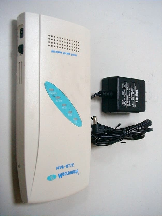
LZU-MAP-811
Macromate Corp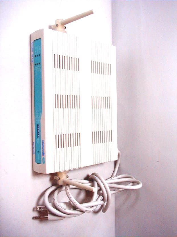
Click to zoom
Application Details
- Equipment Class
- DSS - Part 15 Spread Spectrum Transmitter
- Date of Grant
- Aug 27, 2001
- Application Purpose
- Original Equipment
- Date of Application
- May 15, 2001
- Frequency Range
- 2412.00000000 - 2462.00000000
- Company
- Macromate Corp
- Country
- Taiwan
Documents & Files
Document Text
Text extracted from the exhibit documents filed with the FCC. Open a document above to read the original.
Users Manual
ea101007-q10 (832x1128x24b jpeg)
Attestation Statements
NOTE: 1. The internal PCMCIA wireless lan card move out microstrip Antenna and connect to extension cable . 2. The extension cable connect to mono dipole antenna by SMA connector . 3. The SMA connectors(both male and female) are molding by plastic and permanently fixed on plastic enclosure with two screw on each antenna.
Attestation Statements
The screws are not on the SMA connect. They are on the plastic enclosure as picture. Inject the glue to inside the plastic enclosure, after one or two hours these glue will permanent fixed SMA connector and plastic enclosure.
Block Diagram
Detachable Antenna MMCXConnector MMCXConnector TOKO TDFM1B-2450T-10B 2.45GHz HFA3983 RFPA/DET SOSHIN MDR642E 2.45GHz KDS44MHz MCLK PLL RFVCO 2037.75~ 2109.75 MHz SOSHIN MDR642E SOSHIN MDR642E REFINREFIN REFIN REF_OUT HFA3683A RF/IFCONV SAWTEK 374MHz PLL I/QLO HFA3783QUADIF IFVCO 748.5MHz HFA3841MAC HFA3861BBP RF DAC RF ADC IF DAC I ADC I DAC MOD AND FILTER RAKE AND DEMOD RADIO DATA INTERFACE HOST INTERFACE LOGIC GP SERIAL PORTS MEMORY ACCESS ARBITER EXTERNAL MEMORY RADIO CONTROL PARTS 16-BIT PIPELINED CONTROL PARTS Q DAC TX DAC TX ADC TXALC Q ADC I/O 1 1 7 7 6 6 6 6 6 AGCCTL WEP ENGINE CPU
ID Label/Location Info
LABEL Format: This device complies with Part 15 of the FCC Rules Operation is subject to the following two conditions: (1) This device may not cause harmful interference, and (2) This device must accept any interference received, including interference that may cause undesired operation Model No.:MAP-811 FCC ID:LZU-MAP-811 LABEL Size: 35 x 50 mm LABEL Position: LABEL
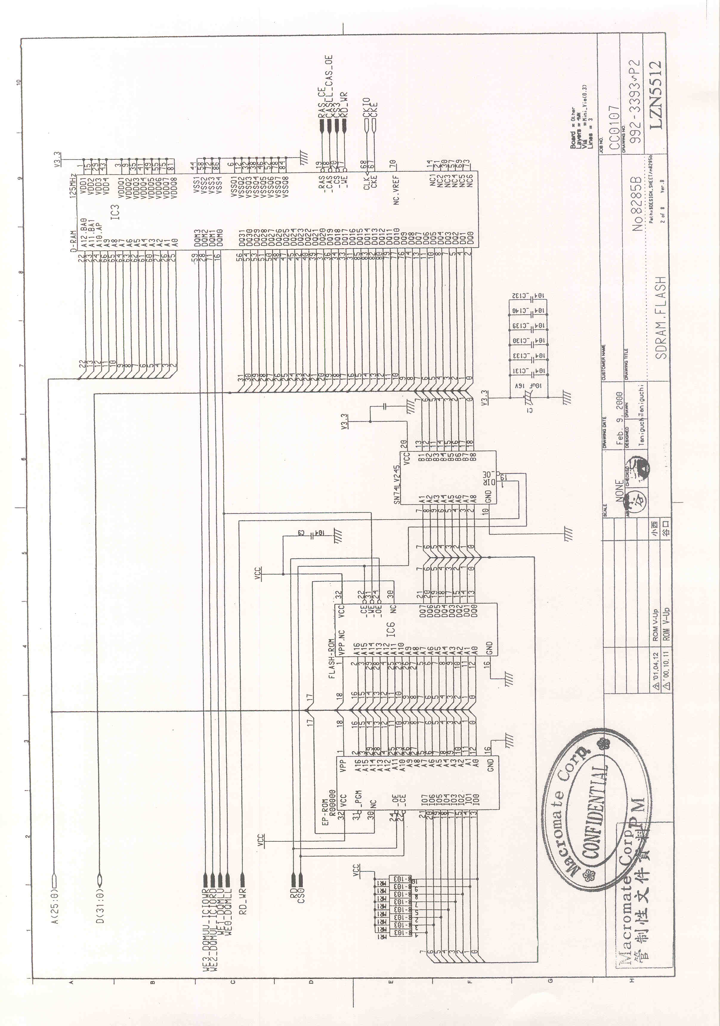
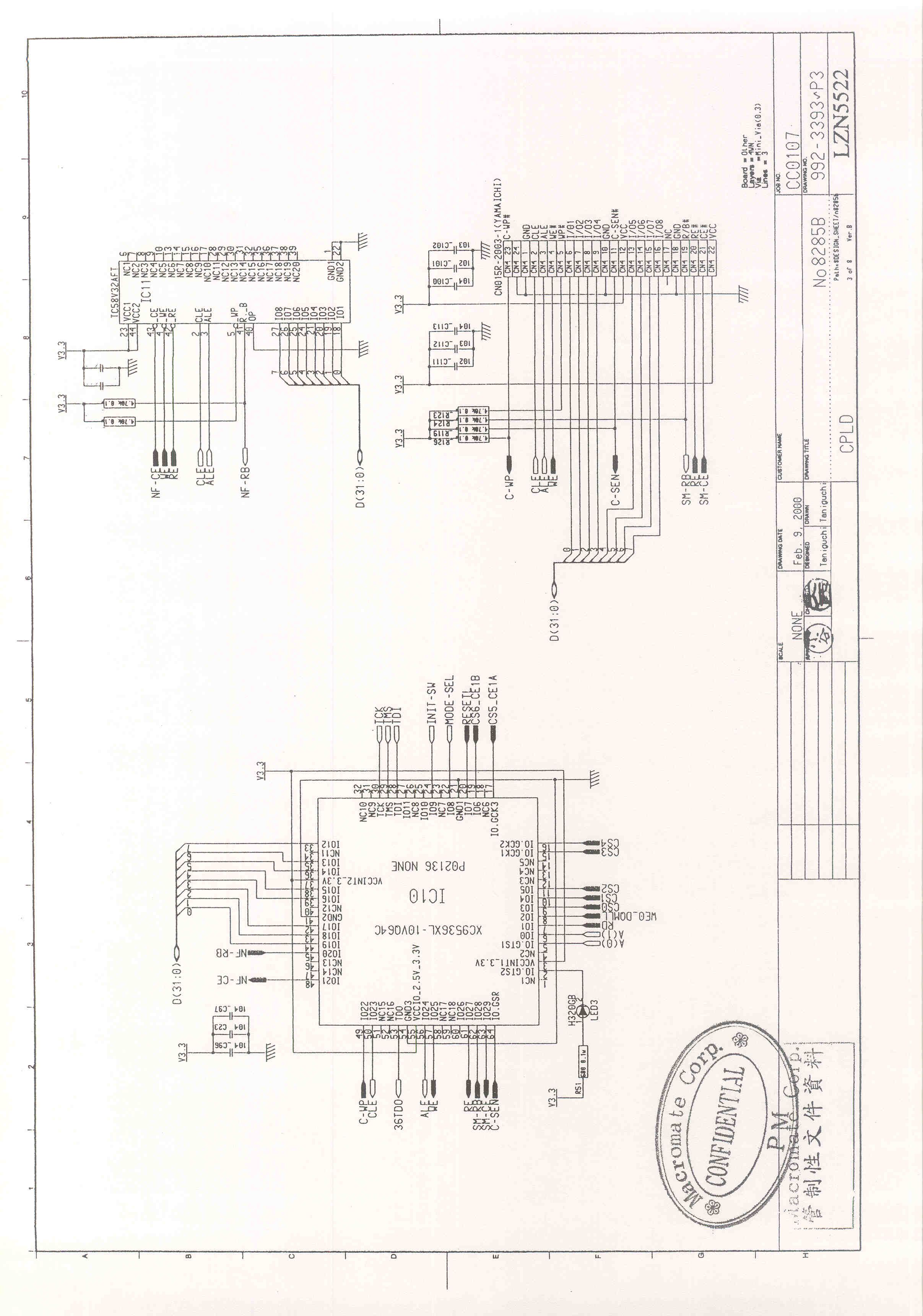
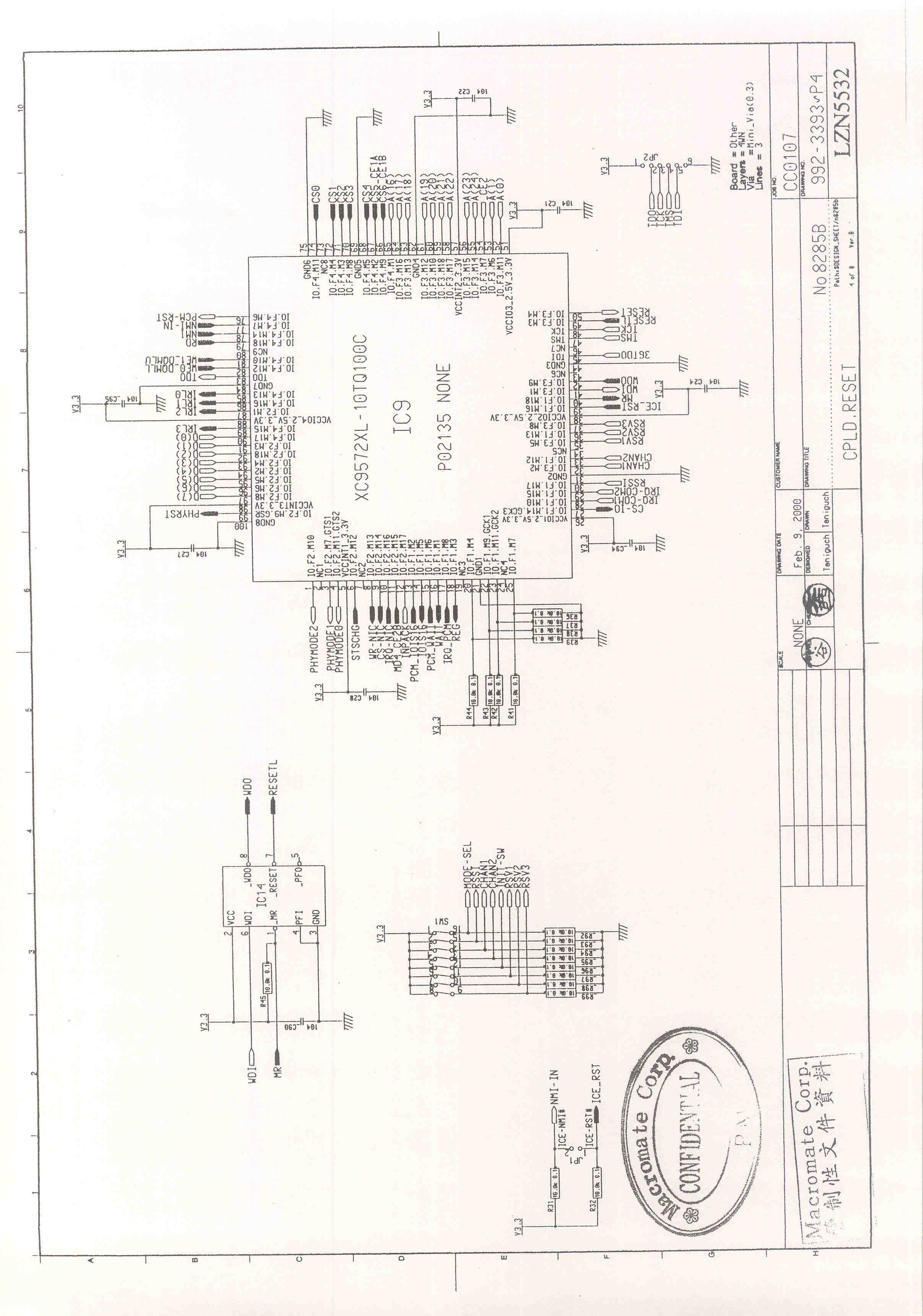
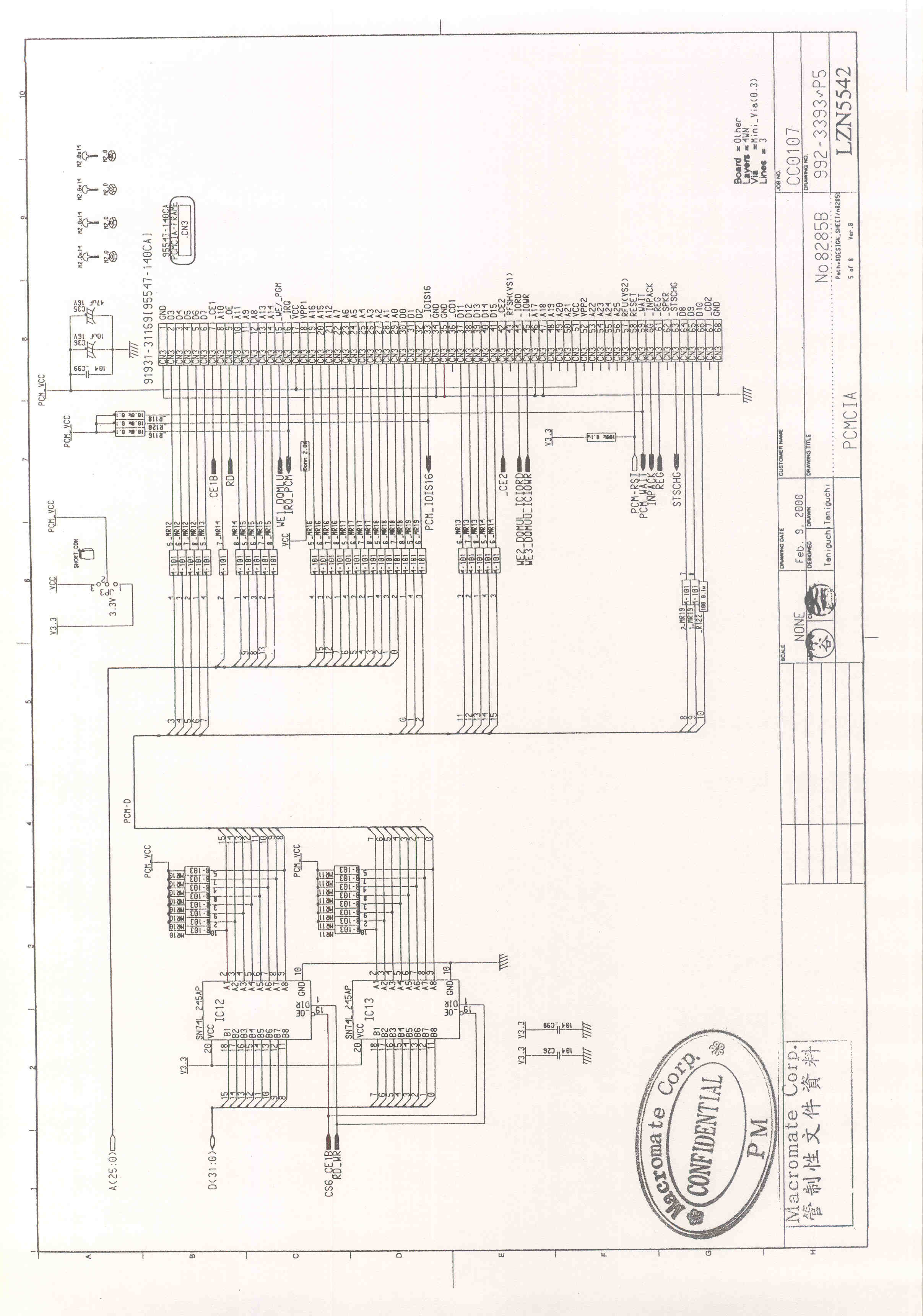
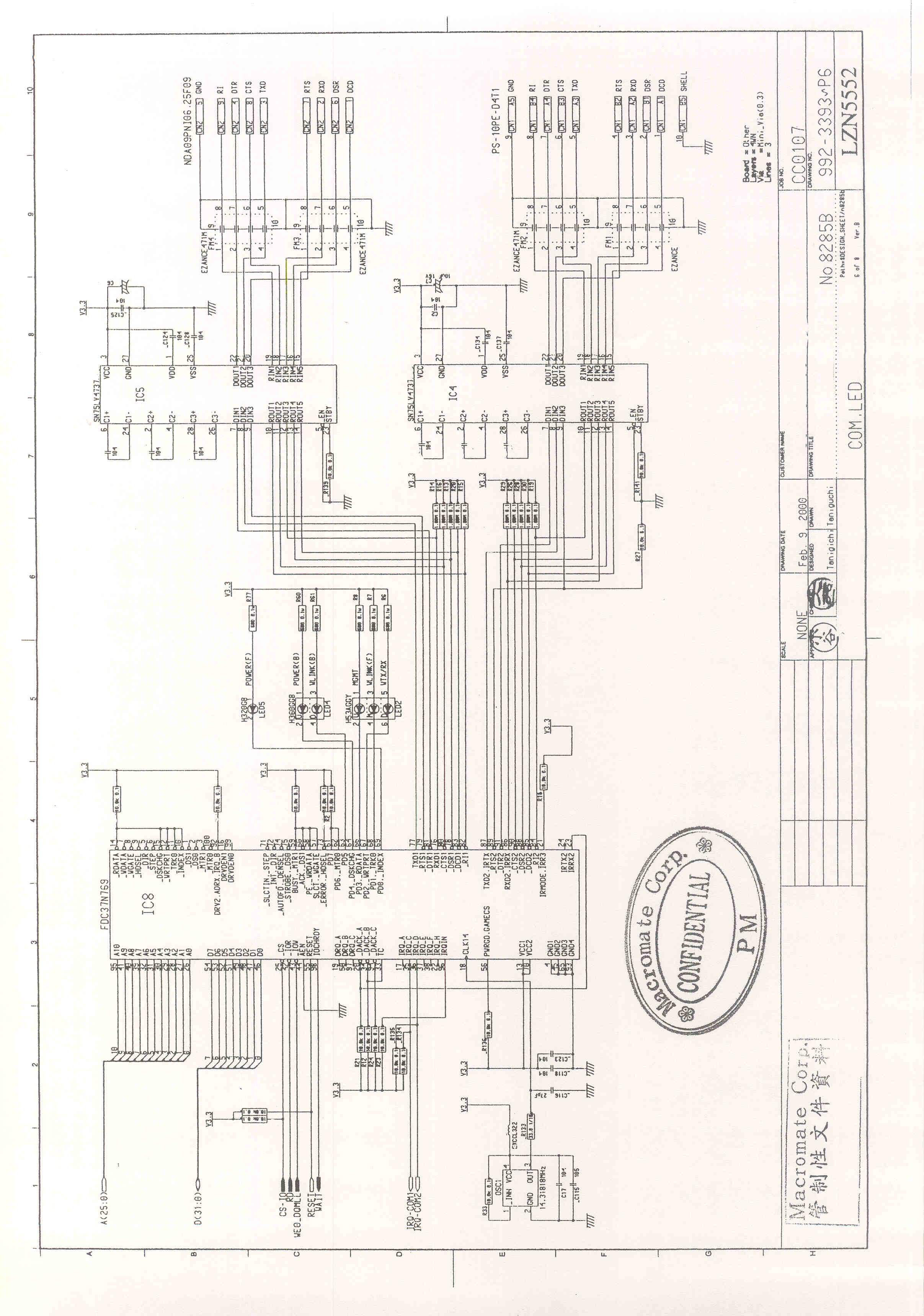
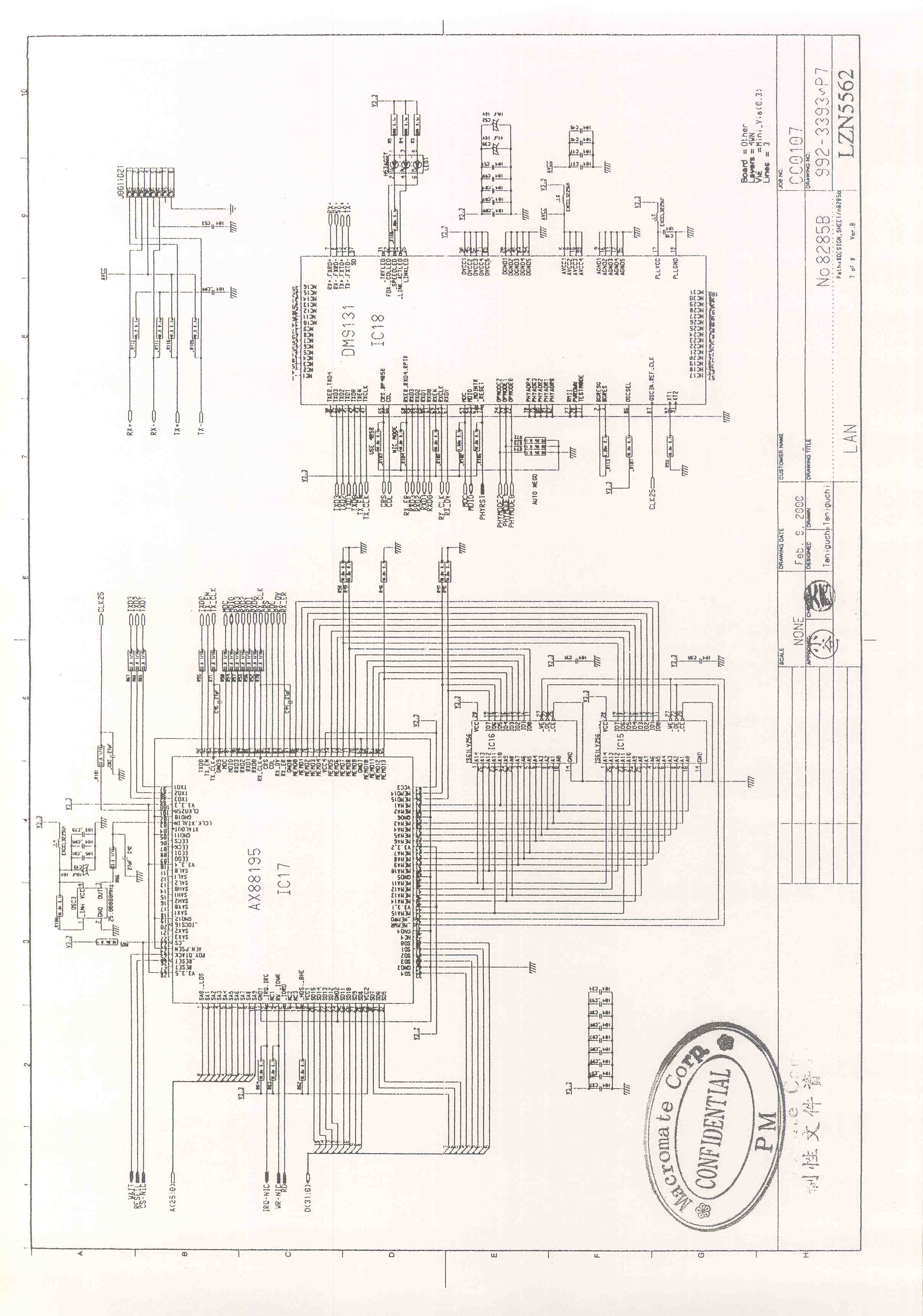
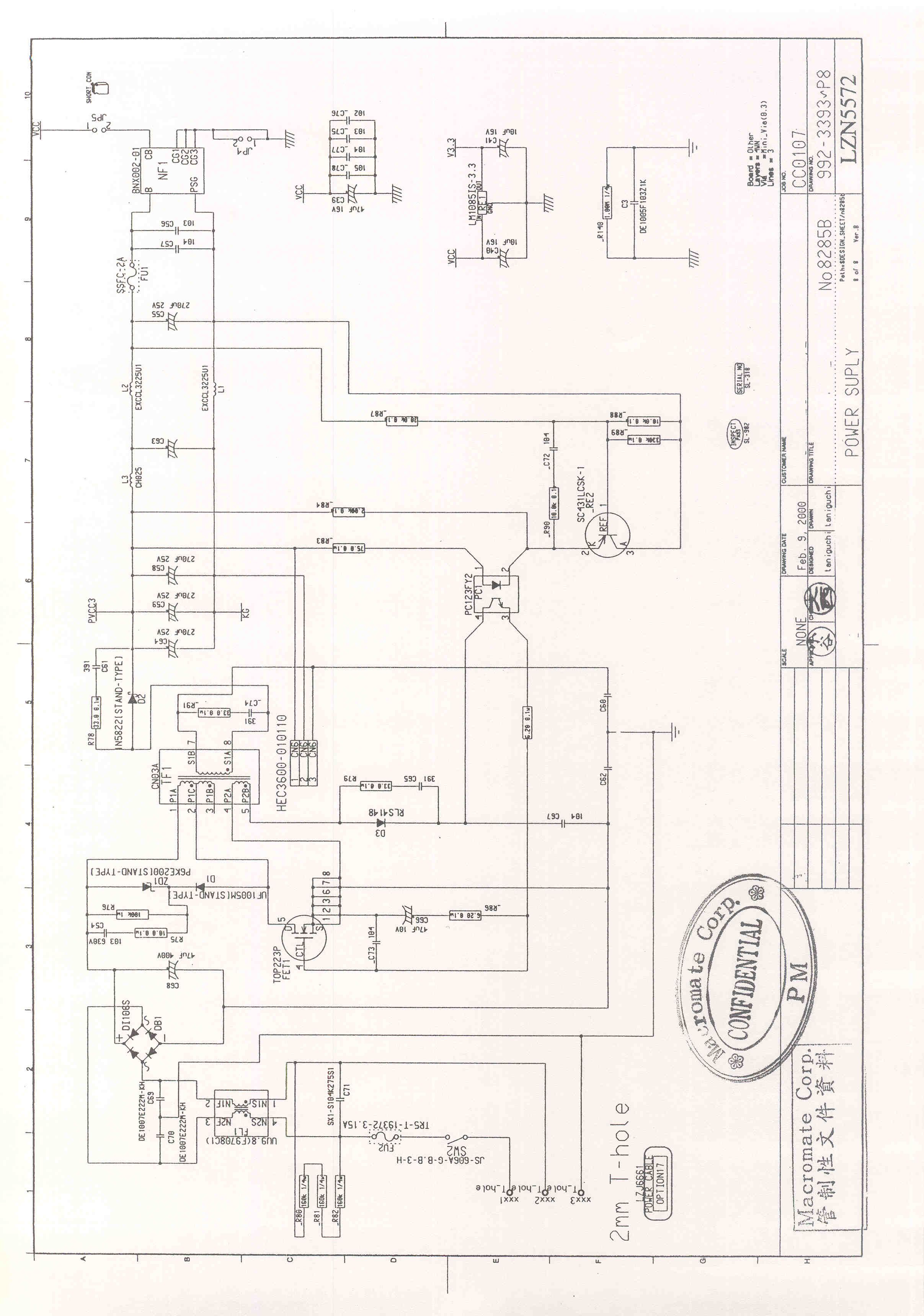
Schematics
123456 A B C D 654321 D C B A Title NumberRevisionSize Orcad C Date:24-May-2001Sheet of File:D:\Zcom Product\0_SCH _PCB\xi300 vb3b\XI300V03B.DDBDrawn By: RESET_BB* TX_CLK S_DATA TX_DATA CSB RX_CLK RX_DATA RX_CLK S_CLK T/R_SW TX_PE LED1 S_CLK MD_RDY XTALI RX_PE MD_RDY RX_PE LE_IF RAMCS* S_DATA RESET_BB* LE_IF RX_DATA LED1 CCA T/R_SW* T/R_SW* XTALI TX_DATA TX_CLK RAMCS* RADIO_PD T/R_SW RADIO_PD CCA TX_PE RAMCS* NVCS* 44MHZ_REF CAL_EN CSBNVCS* CAL_EN MA1 MA11MA9 MA2 MA13 MA14 MA16 MA7 MA14 MA12MA10 MA10 MA8 MA15 MA1 MA10 MA2 MA8 MA15 MA17 MA14 MA6 MA13 MA0 MA6 MA5 MA17 MA1 MA4 MA3 MA11 MA9 MA14 MA12 MA4 MA5 MA12 MA2 MA3 MA8 MA7 MA1 MA6 MA7 MA4 MA17 MA4 MA0 MA8 MA3 MA11 MA0 MA6 MA10 MA15 MA16 MA5 MA9 MA3 MA9 MA0 MA7 MA16 MA11 MA15 MA16 MA12 MA13 MA13 MA5 MA2 MOE* MOE* MWEL* MWEL* MWEL* MOE*MOE* LE_RF SCLK_RF_IF SD_RF_IFSCLK_RF_IF SD_RF_IF LE_RF PA_PE PE2 PE1 PE1PE2 PA_PE MD1 MD7 MD12 MD8 MD14 MD6 MD4 MD6 MD2 MD8 MD3 MD7 MD3MD11 MD15 MD2 MD13 MD5 MD2MD10MD3 MD10 MD6 MD4 MD0 MD5 MD9 MD1MD12MD11 MD0 MD15MD7 MD[0..15] MD14 MD1 MD4 MD0 MD13 MD5 MD9 HCE1* HD12 HRESET HIREQ* HD0 GEN_MODE HA6 HD13 HWE* HREG* HD15 HD3 HD9 HIOWR* HA5 HINPACK* HD10 HD5 HD4 HCE2* HINPACK* HD13 HA4 HD1 HD1 HA1 HA1 HD6 HD14 HSTSCHG* HD6 HWE* HREG* HA3 HD7 HA2 HD0 HA6 HIOWR* HD12 HRESET HA0 HA5 HD2 HA8 HCE2* HIORD* HA0 HD9 HD7 HCE1* HOE* HWAIT* HA9 HA4HA7 HWAIT* HD11 HD3 HIREQ* HA7 HA2 HA8 HA9HA3 HD11 HSTSCHG* HD8 HD2 HD8 HD14 HD15 HD4 HD10 HOE* HD5 HIORD* NC 6 A16 10 A15 11 A12 12 A7 13 A6 14 A5 15 A4 16 A3 17 A2 18 A1 19 A0 20 D0 21 D1 22 D2 23 VSS 24 D3 25 D4 26 D5 27 D6 28 D7 29 /CE 30 A10 31 /OE 32 A11 1 A9 2 A8 3 A13 4 A14 5 VCC 8 /WE 7 NC 9 U2 C7C6 C1 C9C14 C20 C4 C21 C10C5 C2 HCE1_ 1 HD7 2 HD6 3 HD5 4 HD4 5 HD3 6 PJ6 7 PJ5 8 PJ7 9 TCLKIN 10 PL6 11 PL5 12 VSS_CORE3 13 VCC_CORE4 14 PL0 15 RESET 16 TXD 17 TXC 18 RXD 19 RXC 20 PK5 21 PK6 22 PK7 23 VSS_CORE3 24 VCC_CORE3 25 PL2 26 PL1 27 PL3 28 PJ3 29 PJ1 30 PJ0 31 PJ2 32 PK2 33 PK1 34 HSTSCHG_ 36 PK0 35 VSS_CORE3 37 CLKOUT 38 VCC_CORE3 39 XTALI 40 XTALO 41 VSS_IO3 42 PL4 43 MD15 44 MD14 45 MD13 46 MD12 47 MD11 48 MD10 49 MD9 50 MD8 51 VSS_IO3 52 VCC_CORE3 53 MD7 54 MD6 55 MD5 56 MD4 57 MD3 58 MD2 59 MD1 60 MD0 61 TRST_ 62 PK3 63 PK4 64 PJ4 65 VCC_IO3 66 VSS_IO3 67 NVCS_ 68 RAMCS 69 MOE_ 70 MWEL_ 71 MA0 72 MA1 73 MA2 74 MA3 75 MA4 76 MA5 77 MA6 78 MA7 79 MA8 80 MA9 81 VSS_IO3 82 VCC_IO3 83 MA10 84 MA11 85 MA12 86 MA13 87 MA14 88 MA15 89 MA16 90 MA17 91 MA18 92 PL7 93 HD10 94 HD9 95 HD8 96 VSS_IO3 97 VCC_IO3 98 HD2 99 HD1 100 HD0 101 HREG_ 102 HINPACK_ 103 HWAIT_ 104 VCC_IO5 105 HA0 106 HA1 107 HA2 108 HA3 109 HA4 110 HA5 111 HA6 112 HA7 113 HIREG_ 114 VSS_IO3 115 HWE_ 116 HA8 117 HA9 118 HIOWR_ 119 HIOR_ 120 HOE_ 121 HCE2_ 122 HD15 123 VCC_IO3 124 HD14 125 HD13 126 HD12 127 HD11 128 U3 1 2 D4 R42 R12 R6 R4 R7 R8 R79 R16 R3 R1 R2 R14 R18 R10 R5R11R26R17 R21R9 R78 R201 TP 1 T9 21 D1 R72 GND 1 SD3 2 SD4 3 SD5 4 SD6 5 SD7 6 CE1 7 SA10 8 OE 9 SA11 10 SA9 11 SA8 12 SA13 13 SA14 14 WE/PGM 15 IREQ/RDY 16 VCC 17 VPP1 18 SA16 19 SA15 20 SA12 21 SA7 22 SA6 23 SA5 24 SA4 25 SA3 26 SA2 27 SA1 28 SA0 29 SD0 30 SD1 31 SD2 32 IOIS16/WP 33 GND 34 GND 68 CD2 67 SD11 37 SD12 38 SD13 39 SD14 40 SD15 41 CE2 42 RFSH/VS1 43 NC/IOR 44 NC/IOW 45 SA17 46 SA18 47 SA19 48 SA20 49 SA21 50 VCC 51 VPP2 52 SA22 53 SA23 54 SA24 55 SA25 56 NC/VS2 57 RESET 58 WAIT 59 NC/INPACK 60 REG 61 BVD2/SPKR 62 BVD1/STSCHG 63 SD8 64 SD9 65 SD10 66 CD1 36 GND 35 P1 /OE 32 A11 1 A9 2 A8 3 A13 4 /WE 5 CS2 6 A14 11 A12 12 A7 13 A6 14 A5 15 A4 16 A3 17 A2 18 A1 19 A0 20 D0 21 D1 22 D2 23 D3 25 D4 26 D5 27 D6 28 D7 29 /CS1 30 A10 31 GND 24 A15 7 VCC 8 NC 9 (A16) 10 U4 /OE 32 A11 1 A9 2 A8 3 A13 4 /WE 5 CS2 6 A14 11 A12 12 A7 13 A6 14 A5 15 A4 16 A3 17 A2 18 A1 19 A0 20 D0 21 D1 22 D2 23 D3 25 D4 26 D5 27 D6 28 D7 29 /CS1 30 A10 31 GND 24 A15 7 VCC 8 NC 9 (A16) 10 U1 C3 L17 GND 1 VDD 2 VOUT 3 NC 4 CE 5 U202 C19 R213C102 C8 C81 TP 1 L3 C34 GND 1 VDD 2 VOUT 3 NC 4 CE 5 U203 R214C31 R215R216 1 2 D5 R224 R226 44MHZ_REF TX_CLK SCLK_RF_IF TX_PE CCA CSB T/R_SW* CAL_EN TX_DATA RX_DATA LE_RF PE2 RESET_BB* SD_RF_IF LE_IF S_DATA RADIO_PD RX_CLK T/R_SW PA_PE RX_PE MD_RDY PE1 S_CLK A3.3V DVCCS DVCCSDVCCS DVCCS DVCCS DVCCS DVCCS DVCCS DVCCS DVCCS DVCCS DVCCS DVCCS DVCCS DVCCS DVCCS DVCCS DVCCS A3.3V DVCCS 68PIN_VCC DVCCS68PIN_VCC DVCCS 68PIN_VCCA 128K X 8 SRAM128K X 8 SRAM 128K X 8 FLASH DIGITAL POWER PLANE LOCATED CLOSE TO MAC AND SRAM ANALOG/RF POWER PLANE DIGITAL GROUND TIE ANALOG AND DIGITAL GROUND CLOSE TO CONNECTOR JP1 NOTE:HRESET IS ACTIVE HIGH AND TIED HIGH INTERNALLY IN THE HFA3841 (PG 3) (PG 3) (PG 4) (PG 4) (PG 4) (PG 4) (PG 2) (PG 2) (PG 3) (PG 2) (PG 2) (PG 2) (PG 3,4) (PG 3,4) (PG 3,4) (PG 3,4) (PG 2) (PG 2) (PG 2) (PG 1,3) (PG 2) (PG 2) (PG 2) (PG 2) 3.3VOLT LOW VOLTAGE KEYED VS1# CONNECT AGND TO DGND HERE IOIS16 ASSERTED VS2* NOT CONNECTED PULL HIGH (SPKR) WHEN DOWNLOAD FIRMWARE 123456 A B C D 6 54321 D C B A Title NumberRevisionSize Orcad B Date:24-May-2001Sheet of File:D:\Zcom Product\0_SCH _PCB\xi300 vb3b\XI300V03B.DDBDrawn By: TST7TST6TST5 TST4 TST3 TST2 TST1 TST0 TST[0..7] TST7 TST6 TST5 TST4 TST3 TST2 TST1 TST0 VREF RXI+ RXI- RXQ- RXQ+ CSB S_CLK S_DATA TX_CLK REST_BB* TX_PE RX_PE CCA TX_DATA MD_RDY RX_DATA RX_CLK C25 C30 C32 C26 C17 C35 C139 C140 C29 C18 C11C12C15C13 GNDd 1 VDDd 2 SD 3 SCLK 4 R/W 5 CS 6 GNDd 7 VDDd 8 GNDa 9 RX_I+ 10 RX_I- 11 VDDa 12 RX_Q+ 13 RX_Q- 14 GNDa 15 VREF 16 VDDa 17 TX_AGC_IN 18 RX_IF_DET 19 GNDa 20 IREF 21 VDDa 22 TX_I+ 23 TX_I- 24 GNDa 25 COMPCAP2 26 COMPRES2 27 GNDa 28 TX_Q+ 29 TX_Q- 30 VDDa 31 COMPRES1 32 COMPCAP1 33 RX_IF_AGC 34 TX_IF_AGC 35 GNDd 36 VDDd 37 RX_RF_AGC 38 ANT-SEL 39 ANT-SEL 40 BYP 41 MCLK 42 GNDd 43 TEST0 44 TEST1 45 TEST2 46 TEST3 47 TEST4 48 TEST5 49 TEST6 50 TEST7 51 RXCLK 52 RXD 53 MD_RDY 54 TXCLK 55 GNDd 56 VDDd 57 TXD 58 TX_RDY 59 CCA 60 RX_PE 61 TX_PE 62 RESET 63 SDI 64 U5 C36 TP 1 T7 TP 1 T6 TP 1 T5 TP 1 T4 TP 1 T3 TP 1 T2 TP 1 T1 TP 1 T8 R34R33R32 R30R28 R20 R27 R29 R23 R19 R22 R13 TP 1 T11 TP 1 T10 TP 1 TP209 TP 1 TP208 TP 1 TP207 TP 1 TP206 ANTSEL TX_DET IF_DE…
Text truncated - open the document above for the full version.
Test Report
Test Repot ----------------------------------------------------------------------------------- 1/89 Report No.: MA115118 Training Research Co., Ltd., TEL:886-2-26935155, Fax:886-2-26934440 MEASUREMENT REPORT of WIRELESS LAN Applicant: Macromate Corp. Model No.:MAP-811 EUT:Wireless Bridge Router FCC ID:LZU-MAP-811 Report No.:MA115118 Test by : Training Research Co., Ltd. TEL : 886-2-26935155 FAX : 886-2-26934440 2, Lane 194, Huan-Ho Street, Hsichih, Taipei Hsien 221, Taiwan, R.O.C. Test Repot ----------------------------------------------------------------------------------- 3/89 Report No.: MA115118 Training Research Co., Ltd., TEL:886-2-26935155, Fax:886-2-26934440 Tables of Contents I. GENERAL ............................................................................................................................. 5 1.1 Introduction ........................................................................................................................ 5 1.2 Description of EUT ............................................................................................................ 5 1.3 Description of Support Equipment ...................................................................................... 5 1.4 Configuration of System Under Test .................................................................................... 7 1.5 Verify the Frequency and Channel ...................................................................................... 8 1.5.1 Verify the Frequency Pairs ............................................................................................... 8 1.6 Test Procedure ................................................................................................................... 9 1.7 Location of the Test Site ..................................................................................................... 9 1.8 General Test Condition ....................................................................................................... 9 II. Section 15.207: Power line conducted emissions for AC powered units ........................... 10 2.1 Test Condition & Setup .................................................................................................... 10 2.2 List of Test Instruments ..................................................................................................... 10 2.3 Test Configuration ............................................................................................................ 11 2.4 Test Result of Conducted Emissions .................................................................................. 13 2.4.1 EUT Station Transmit Only ............................................................................................ 13 III. Section 15.247(a)(2): Bandwidth for direct sequence system ............................................ 19 3.1 Test Condition & Setup .................................................................................................... 19 3.2 Test Instruments Configuration .......................................................................................... 19 3.3 List of Test Instruments ..................................................................................................... 19 3.4 Test Result of Bandwidth .................................................................................................. 20 IV. Section 15.247(a) (2) : Power Output .................................................................................. 27 4.1 Test Condition & Setup .................................................................................................... 27 4.2 List of Test Instruments ..................................................................................................... 28 4.3 Test Result of Fundamental Emission ................................................................................. 29 Test Repot ----------------------------------------------------------------------------------- 4/89 Report No.: MA115118 Training Research Co., Ltd., TEL:886-2-26935155, Fax:886-2-26934440 V. Section 15.247(c) (2) : Spurious Emissions (Radiated) .................................................... 30 5.1 Test Condition & Setup .................................................................................................. 30 5.2 List of Test Instruments ................................................................................................... 31 5.2.1 Duty Cycle Factor Measurement ................................................................................. 31 5.3 Test Instruments Configuration ........................................................................................ 33 5.4 Test Result of Second Harmonic ..................................................................................... 35 5.5 Test Result of Spurious Radiated Emissions ..................................................................... 36 5.5.1 Base and Handset Station Transmit Only ...................................................................... 36 VI. Section 15.247(d) : Power Spectral Density ..................................................................... 60 6.1 Test Condition & Setup .................................................................................................. 60 6.2 Test Instruments Configuration ........................................................................................ 61 6.3 List of Test Instruments.................................................................................................... 61 6.4 Required of Carrier Frequency ....................................................................................... 62 6.5 Test Result of Power Spectral Density ............................................................................ 64 VII. Section 15.247(e): Processing Gain .................................................................................. 71 7.1 Test Method…
Text truncated - open the document above for the full version.
Test Report
Test Setup for Conducting Peak Power List of Test Instruments Instrument Name Model No. Brand Serial No. Last time Next time Power Meter E4418B HP GB39291240 Sep.11.2000 Sep.10.2001 Power Sensor E4413A HP US37181867 Sep.11.2000 Sep.10.2001 Splitters & Combiner ZAPD-4 Mini-Circuits NA NA NA Test Data Channel Average Power (dBm) Peak Power (dBm) CH1 5.3dBm 16.38dBm CH6 7.2dBm 18.28dBm CH11 7.8dBm 18.08dBm Note: 1. Duty Cycle factor as original test report page 31. 2. Maximum Peak power = Average Power + Duty Cycle factor = 7.8 + 11.08 = 18.08 dBm notebook EUT Power Meter Splitters & Combiner
Test Report
Power Spectral Density HP8594A Spectrum Analyzer Fig 12. Test Configuration of power spectral density P.S.COM port to COM port from notebook computer to control the EUT at maximal power output and channel Number. 6.3 List of Test Instruments Instrument Name Model No. Brand Serial No. Last time Next time Spectrum Analyzer 8594A H P 3710A00279 10/18/00 10/18/01 Combiner ZAPD-4 Mini Circuits N/A N/A N/A Test Result of Power spectral density Channel Frequency (GHz) Ppr (dBm) AC/DC Adaptor 01 2.410 -11.10 AC/DC Adaptor 06 2.435 -12.62 AC/DC Adaptor 11 2.460 -9.44 AC Power Source 01 2.412 -11.88 AC Power Source 06 2.437 -12.03 AC Power Source 11 2.460 -10.35 Note: 1. Ppr: spectrum read power density (using peak search mode), Ppq: actual peak power density in the spread spectrum band. AC Source Adaptor EUT NOTEBOOK AC/DC Adaptor CH01 AC/DC Adaptor CH06 AC/DC Adaptor CH11 AC Adaptor CH1 AC Adaptor CH6 AC Adaptor CH11
Test Report
Section 15.247(e): Processing Gain Test Instruments Configuration Figure 1 Shielding Room 51dB Power Meter Reading Attenuator Test Configuration of processing gain List of Test Instruments Instrument Name Model No Brand Serial No. Last time Next time Signal Generator 83711A HP 3429A00434 05/19/00 05/19/01 Power Meter E4418B HP GB39291240 09/11/00 09/11/01 Combiner 15542 ZAPD-4 Mini Circuits N/A N/A N/A Attenuator (6dB to 18 GHz) MCL BW-S6W2 Mini Circuits Reference HD 83711A Signal Generator Splitter& Combiner EUT HP E4418B. Power 18dB Attenuator Splitter& Combiner Bit Error Rate (BER) (1) Test Background and procedure According to FCC regulation, a direct sequence spread spectrum system must have processing gain , P G of the least 10 dB. Compliance to this requirement can be shown by demonstrating a relative bit-error-ratio (BER) performance improvement (and corresponding signal to noise ratio per symbol improvement of at least 10dB )between the case where spread spectrum processes (coding, modulation) are engaged relative to the processes being bypassed. In some practical system, the spread spectrum processing cannot simply bypassed. In accordance with the new NPRM 99-231, if the vendor has a system with less than 10 chips per symbol, the CW jamming results must be supported by a theoretical explanation of the system processing gain. (2) Theoretical calculations The processing gain is related to the jamming margin as follows: system output p L S J N S + + =G Where REFERENCE BER is the reference bit error ratio with its corresponding, theoretical output signal to noise ratio per symbol, () output N S , () S J is the jamming margin (jamming signal power relative to desired signal power),and system L are the system implementation losses. The maximum allowed total system implementation loss is 2 dB. The HFA3861A direct sequence spread spectrum base band processor uses CCK modulation, which is a form of M-ray Orthogonal Keying. The BER performance curve is given by: The probability of error for generalized M-ary Orthogonal signaling using coherent demodulation is given by: dz Z E zQP N S M b ce − +−−=−= ∫ ∞ − − 2 exp212 2 1 11P 2 1 2 1 0 01 η π This integral cannot be solved in closed form, and numerical integration must be used. This is done in a MATHCAD environment and is displayed in graphical format The reference PER is specified as 8% . When operating DQPSKCCK at 11Mbps, the corresponding Es/No (signal to noise ratio per symbol) is 16.4 dB. The Es/No required to achieve the desired BER with maximum system implementation losses is 18.4dB. The minimum processing gain is again, 10dB, therefore: dB S J dBdBL S J N E system output o s p 100.24.16G≥ ++=+ + = dB S J dBG p 104.18≥ += The minimum jammer to signal ratio is as follow: dB4.8 S J −≥ =16.4dB =18.4 2 10 − 0 10 − Es/No (dB) Thermal Noise 1000 byte Packet Error Rate 1000 byte PER vs. Es/No 15.5 16 16.5 17 7.4 Test Procedure The test block diagram in the figure (1) and the procedure as below. (1) Install two lan card into PC. (2) Install DOS Test into computers for E.U.T. and Reference. (3) Set the two LAN card of computer as “Port1 ping Port2”. (4) Generated the Log File in the Reference Port1 of computer and send the test file. (5) The port 1of pc (Reference) send 1000 packet to EUT. Then EUT response to Port 2 of PC. Also, PC can calculated packet data bit error rate. (6) Ensure that CW Jammer generator RF out put is disabled and measure the power at the power meter port using the power meter 1. This is the relative signal power, r S. (7) Set CW Jammer generator RF output frequency equal to the carrier frequency and enable generator output Set reference CW Jammer power level at power meter port 8.4 dB below r S (minimum J/S, or 10 dB processing gain reference level).Note the power level setting on the generator, this is the reference CW Jammer power setting, r J(Power Meter 2) . (8) Enable CW Jammer at the reference power level and verify that the PER test indicates a per of less than 8%. (9) Alternatively, adjust the CW Jammer level to that which causes 8% PER and verify that the S/J is less than 8.4dB. (10) Repeat step 7 for uniform steps in frequency increments of 50kHz across the receiver passband with the CW Jammer. In this case the receiver passband is 5.0MHz. The number of points where the PER fail to achieve 8% (is higher than 8%) is determined and if this is above 20% of the total, the test is failed otherwise it is passed. The margin by which the radio passes the test (for information purposes) can be determined from the average of the remaining points’ PERs scaled on the PER curve above. Test Result summary Date rate Channel number Process gain(dB) 2M 6 12.3(dB) 11M 6 11.3(dB) NOTE: 1.S = Power Meter Reading + Duty Cycle factor 2.N = Power Meter Reading when S turn off. ........ DQPSK Gp = (S/N 0) + Mj +Lsys Gp = 12.6 + Mj + 2 Gp = 14.6 + Mj DQPSK CCK Gp = (S/N 0) + Mj +Lsys Gp = 16.4 + Mj + 2 Gp = 18.4 + Mj 7.5 Test Result of Processing Gain 2440.0 0.0 2440.0 24Table 1 Processing Gain [Channel 6, CCK 11Mbps, 2.43205GHz to 2.44205GHz] Jammer Frequency (MHz) Signal Level S (dBm) Signal Generator RF Output J (dBm) Mj (J/S) Process Gain (dB) 2440.0 2432.05 -12.2 -16.05 -3.85 14.55 2432.10 -12.2 -16.53 -4.33 14.07 2432.15 -12.2 -16.75 -4.55 13.85 2432.20 -12.2 -16.55 -4.35 14.05 2432.25 -12.2 -16.42 -4.22 14.18 2432.30 -12.2 -16.88 -4.68 13.72 2432.35 -12.2 -16.62 -4.42 13.98 2432.40 -12.2 -16.02 -3.82 14.58 2432.45 -12.2 -16.88 -4.68 13.72 2432.50 -12.2 -16.62 -4.42 13.98 2432.55 -12.2 -16.49 -4.29 14.11 2432.60 -12.2 -16.9 -4.7 13.7 2432.65 -12.2 -16.88 -4.68 13.72 2432.70 -12.2 -17.03 -4.83 13.57 2432.75 -12.2 -17.05 -4.85 13.55 2432.80 -12.2 -17.44 -5.24 13.16 2432.85 -12.2 -17.16 -4.96 13.44 2432.90 -12.2 -17.44 -5.24 13.16 2432.95 -12.2 -18 -5.8 12.6 2433.00 -12.2 -17.49 -5.29…
Text truncated - open the document above for the full version.
Test Report
About Certification or DOC for MAP-811. The subjective device is not Class B digital device, The RS-232 connector on the subjective device is for subjective device installation initial setting, please reference as user manual page 34 section 5.1 setting for telnet/ console management. In the normal use condition, The RS-232 connector will not connect to any cable, only RJ45( Ethernet cable ) and power cord are connected to the subjective device.
Test Report
Test Setup for Conducting Peak Power Test Procedure: 1. 2. 3. 1. The output of the transmitter thought 30dB attenuator and terminated by Schottkey Detector Diode (Hewlett- Packard HSMS-2850) 2. The output of the Shocttkey Diode Detector connected to the vertical channel of an oscilloscope. The observed trace of the oscilloscope shall be recorded as "A". 3. The combination of the diode detector and the oscilloscope capable of faithfully reproducing the envelop peaks and the duty cycle of the transmitter output signal. 4.The transmitter replaced by a signal generator . The output frequency of the signal made equal to the center of the frequency range occupied by the transmitter and unmodulated. 5.The output of the signal generator raised to reach the peak of trace "A" and then replace the 30 db attenuator and Schottkey Detector Diode by power meter, measure the signal generator output level record as x mW. 6. The signal generator output level XmW is the transmitter output peak power. Recording the following. Test Data Channel Output peak power (mw) CH1 6.35 CH6 6.59 CH11 6.01 30dB ATT EUT HSMS-2850 Oscilloscope 30dB ATT HSMS-2850 Oscilloscope Signal Generator Signal Generator Power Meter
Test Report
Section 15.247(e): Test Setup for Conducting Processing Gain Test Instruments Configuration Shielding Room 42dB Attenuator Test Configuration of processing gain Figure 1 Note: 1. Corrected the Schottkey Detector Diode (Hewlett-Packard HSMS-2850) and Oscilloscope as Peak Power Meter. The corrected procedure same as Conducting Peak power measurement. Reference HD 83711A Signal Generator Splitter& Combiner EUT Peak power meter 9dB Attenuator Splitter& Combiner Bit Error Rate (BER) (1) Test Background and procedure According to FCC regulation, a direct sequence spread spectrum system must have processing gain , P G of the least 10 dB. Compliance to this requirement can be shown by demonstrating a relative bit-error-ratio (BER) performance improvement (and corresponding signal to noise ratio per symbol improvement of at least 10dB) between the cases where spread spectrum processes (coding, modulation) are engaged relative to the processes being bypassed. In some practical system, the spread spectrum processing cannot simply bypassed. In accordance with the new NPRM 99-231, if the vendor has a system with less than 10 chips per symbol, the CW jamming results must be supported by a theoretical explanation of the system processing gain. (2) Theoretical calculations The processing gain is related to the jamming margin as follows: system output p L S J N S + + =G Where REFERENCE BER is the reference bit error ratio with its corresponding, theoretical output signal to noise ratio per symbol, () output N S , () S J is the jamming margin (jamming signal power relative to desired signal power),and system L are the system implementation losses. The maximum allowed total system implementation loss is 2 dB. The HFA3861A direct sequence spread spectrum base band processor uses CCK modulation, which is a form of M-ray Orthogonal Keying. The BER performance curve is given by: The probability of error for generalized M-ary Orthogonal signaling using coherent demodulation is given by: dz Z E zQP N S M b ce − +−−=−= ∫ ∞ − − 2 exp212 2 1 11P 2 1 2 1 0 01 η π This integral cannot be solved in closed form, and numerical integration must be used. This is done in a MATHCAD environment and is displayed in graphical format The reference PER is specified as 8% . When operating CCK at 11Mbps, the corresponding Es/No (signal to noise ratio per symbol) is 16.4 dB. The Es/No required to achieve the desired BER with maximum system implementation losses is 18.4dB. The minimum processing gain is again, 10dB, therefore: dB S J dBdBL S J N E system output o s p 100.24.16G≥ ++=+ + = dB S J dBG p 104.18≥ += The minimum jammer to signal ratio is as follow: dB4.8 S J −≥ =16.4dB =18.4 2 10 − 0 10 − Es/No (dB) Thermal Noise 1000 byte Packet Error Rate 1000 byte PER vs. Es/No 15.5 16 16.5 17 7.4 Test Procedure The test block diagram in the figure (1) and the procedure as below. (1) Install two Lan card into PC. (2) Install DOS Test software into computers for E.U.T. and Reference. (3) Set the two LAN card of computer as “Port1 ping Port2”. (4) Generated the Log File in the Reference Port1 of computer and send the test file. (5) The port 1of pc (Reference) send 1000 packet to EUT. Then EUT response to Port 2 of PC. Also, PC can calculated packet data bit error rate. (6) Ensure that CW Jammer generator RF out put is disabled and measure the power at the power meter port using the peak power meter. This is the relative signal power, r S. (7) Set CW Jammer generator RF output frequency equal to the carrier frequency and enable generator output Set reference CW Jammer power level at power meter port 8.4 dB below r S (minimum J/S, or 10 dB processing gain reference level).Note the power level setting on the generator, this is the reference CW Jammer power setting, r J (8) Enable CW Jammer at the reference power level and verify that the PER test indicates a per of less than 8%. (9) Alternatively, adjust the CW Jammer level to that which causes 8% PER and verify that the S/J is less than 8.4dB. (10) Repeat step 7 for uniform steps in frequency increments of 50kHz across the receiver passband with the CW Jammer. In this case the receiver passband is 5.0MHz. The number of points where the PER fail to achieve 8% (is higher than 8%) is determined and if this is above 20% of the total, the test is failed otherwise it is passed. The margin by which the radio passes the test (for information purposes) can be determined from the average of the remaining points’ PERs scaled on the PER curve above. Test Result summary Date rate Channel number Process gain(dB) 2M 6 11.55(dB) 11M 6 11.39(dB) . ........ DQPSK Gp = (S/N 0) + Mj +Lsys Gp = 12.6 + Mj + 2 Gp = 14.6 + Mj CCK Gp = (S/N 0) + Mj +Lsys Gp = 16.4 + Mj + 2 Gp = 18.4 + Mj Test Result of Processing Gain 2440.0 0.0 2440.0 24Table 1 Processing Gain [Channel 6, CCK 11Mbps, 2.43205GHz to 2.44205GHz] Jammer Frequency (MHz) Signal Level S (dBm) Signal Generator RF Output J (dBm) Mj (J/S) Process Gain (dB) 2440.0 2432.05 -8.27-12.91-4.6413.76 2432.10 -8.27-12.52-4.2514.15 2432.15 -8.27-13.14-4.8713.53 2432.20 -8.27-12.98-4.7113.69 2432.25 -8.27-12.78-4.5113.89 2432.30 -8.27-13.57-5.313.1 2432.35 -8.27-13.49-5.2213.18 2432.40 -8.27-12.61-4.3414.06 2432.45 -8.27-13.65-5.3813.02 2432.50 -8.27-13.2-4.9313.47 2432.55 -8.27-12.83-4.5613.84 2432.60 -8.27-13.57-5.313.1 2432.65 -8.27-12.85-4.5813.82 2432.70 -8.27-13.75-5.4812.92 2432.75 -8.27-13.39-5.1213.28 2432.80 -8.27-13.9-5.6312.77 2432.85 -8.27-13.87-5.612.8 2432.90 -8.27-14.31-6.0412.36 2432.95 -8.27-14.41-6.1412.26 2433.00 -8.27-14.35-6.0812.32 2433.05 -8.27-13.75-5.4812.92 2433.10 -8.27-13.65-5.3813.02 2433.15 -8.27-13.54-5.2713.13 2433.20 -8.27-14.05-5.7812.62 2433.25 -8.27-14.73-6.4611.94 2433.30 -8.27-14.05-5.7812.62 2433.35 -8.27-14.21-5.9412.46 2433.40 -8.27-14.41-6.1412.26 2433.45 -8.27-14.8-6.5311.87 243…
Text truncated - open the document above for the full version.
Test Report
As your e-mail dated june,21, we have tested the EUT antenna gain as following (this page ). The antenna dimension and the photo as next pages. The plot indicate the dBm axial value right side. We used the substitution method compare to the other reference Horn Antenna, the reference level for 0dBi is –5dBm. Antenna Specification : Model NO. W250-0101B Antenna Type. Mono Dipole Antenna Antenna Gain 1.82dBi
Test Report
RF SAFETY MPE calculation for this wall mounted Mobile device (greater than 20 cm ) According to OET BULLETIN 56 Fourth Edition / August 1999, Equation for Prediction RF Fields: P G 6.59 x 1.584 2 S = S = = 0.00207 mW / cm 2 2 4 4
Test Report
12mW output peak power in original report was measured by Spectrum Analyzer radiated test method.64mW was measured by average power meter plus duty cycle correction factor. (11.08dB).6.59mw was measured by Schottkey Diode Detector and 30dB attenuator was too large , caused scope plot loss the dynamic range. As your command we have reduced the attenuator to 12dB and improved our Diode Detector with Matching Network and 100K resistive load the schematic drawing as figure 1, the real body as figure 2, the EUT output power waveform as figure 3, and Signal Generator calibration as figure 4. Test setup for conducting peak power as page 3. Curre…
Text truncated - open the document above for the full version.
Contact Information
Applicant
Jerry Siy
Technical Contact
TRAINING RESEARCH CO., LTD.JACK TSAI
[email protected]886-2-26935155
NO. 2, LANE 194, HUAN-HO STREET. · TAIPEI HSIEN, · Taiwan
Non-Technical Contact
TRAINING RESEARCH CO., LTD.JACK TSAI
[email protected]886-2-26935155
Test Firm
Training Research Co., Ltd.Jack Tsai
Technical Specifications
| # | Rule Parts | Frequency Range | Power Output |
|---|---|---|---|
| 1 | 15C | 2.41 GHz - 2.46 GHz | 48.00 mW |
Other Applications from Macromate Corp
LZU-MAP-811E-
Sep 11, 2001Wireless Access Point
Equipment Class
DTS - Digital Transmission SystemLZUMH812
Feb 28, 1996Ethernet Hub
Equipment Class
JBP - Part 15 Class B Computing Device PeripheralLZUMN200CT
Jan 16, 1995Ethernet LAN Card
Equipment Class
JBP - Part 15 Class B Computing Device Peripheral