ML9FM250EBroadcast FM Exciters
Ptek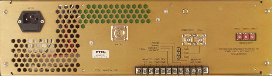
Click to zoom
Application Details
- Equipment Class
- TBC - Licensed Broadcast Station Transmitter
- Date of Grant
- Feb 08, 2005
- Application Purpose
- Original Equipment
- Date of Application
- Feb 08, 2005
- Equipment Note
- Broadcast FM Exciters
- Frequency Range
- 88.00000000 - 108.00000000
- Company
- Ptek
- Country
- United States
Documents & Files
Document Text
Text extracted from the exhibit documents filed with the FCC. Open a document above to read the original.
Users Manual
HANDBOOK BROADCAST FM EXCITERS FM25E FM50E FM150E FM250E FM SERIES PTEK Limited Warranty PTEK (SELLER) warrants that products are free from defects in material and workmanship and meet performance specifications provided, however, that: (A) SELLER’ liability under this Warranty is limited to repairing or replacing, at its option, any product delivered here under not conforming to this Warranty; (B) This Warranty is limited to a period of two years; (C) Minor deviations from specifications which do not affect performance are excluded from this Warranty; and (D) SELLER shall be liable under this Warranty only if: (1) It is promptly notified in writing by the Buyer upon discovery of the failure of any product to conform to this Warranty, (2) The product is returned to SELLER, transportation charges prepaid by the Buyer, (3) The product is received by SELLER not later than ten days after the last day of the two-year period of this Warranty, and (4) SELLER’ examination of the Product discloses to SELLER’S reasonable satisfaction that such defects or failures as may exist have not been caused by misuse, neglect, improper installation, repair, alteration, accident or shipping. The Buyer will prepay freight to and from SELLER on products serviced here under at SELLER’ plant; but SELLER may, at its option, elect to perform any repairs here under at the Buyer’s place of business. The foregoing constitutes SELLER’S entire Warranty expressed, implied and/or statutory, except as to title, and states the full extent of SELLER’S liability to the Buyer or to any other party for any breach of such Warranty and for damages, whether direct, special, incidental or consequential; and, other than as expressly provided in this document. No Warranties, expressed or implied, including any Warranty or merchant ability or of fitness for a particular purpose, are made. No employee, representative or agent of SELLER has any authority, expressed or implied, to alter or to supplement the terms of this Warranty. Warranty Service The Limited Warranty covers parts and labor to the original purchaser for two year. Damage caused by misuse or shipping is excluded from the warranty. Before returning units or material, contact the factory for a Returned Material Authorization (RMA) number. Ship all material prepaid. Defective material should be addressed to: PTEK Customer Service Manager 1814 Schooldale Drive San Jose, CA. 95124 (408) 448-3342 Page 3 Contents Safety Notice .................................................................................................................4 Rear FCC, Accessory Connections & efficiency V O/P Pwr.................................................12 Parts list Chassis...........................................................................................................22 Parts list Synth Board ..................................................................................................25 Parts list LED Board ....................................................................................................25 Specifications ................................................................................................................5 Front &Panel Layout .............................................................................................6 Installation .....................................................................................................................8 Schematic Synthesizer ...........................................................................................12-13 PROVISIONAL......................11/25/96 REV A.....................................1/16/97 REV B.....................................10/7/97 REV C.....................................4/13/99 REV D.....................................5/24/99 REV E....................................12/14/99 REV G........................................7/7/03 Rev record Safety BEFORE APPLYING POWER GROUND THE EXCITOR. Fuses . DO NOT OPERATE IN AN EXPLOSIVE ATMOSPHERE DO NOT REMOVE THE EXCITOR COVER Output connector Verify that the line voltage is 115V To minimize shock hazard, the excitor chassis must be connected to an electrical ground. the excitor must be connected to the ac power mains through a three-conductor power cable, with the third wire firmly connected to an electrical ground (safety ground) at the power outlet. Any interruption of the protective (grounding) conductor or disconnection of the protective earth terminal will cause a potential shock hazard that could result in personal injury. If the excitor is to be energized by any other source be certain the that chassis is connected to a separate safety ground. Only fuses with the same required current, voltage rating, and specified type (normal blow, time delay, etc.) should be used. Do not use repaired fuses or short-circuited fuseholders. To do so could cause a shock or fire hazard Do not operate the power amplifier in the presence of flammable gases or fumes. Operating personnel must not remove the exciter cover. Component replacement and internal adjustments must be made only by qualified service personnel. The type N output connector carries dangerously high RF voltages which present a shock and burn hazard. operate this excitor with out the out put connector properly terminated in either an adequately rated load or antenna. NEVER Page 4 Specifications MONAURAL Audio Input Impedance: Audio Input Level: Audio Frequency Response: Total Harmonic Distortion: FM S/N Ratio (FM Noise): Asynchronous AM S/N Ratio (AM Noise): Synchronous AM SIN Ratio (Incidental AM Noise): 600 ohms, balanced +10 dBm (6.93 volts peak-to-peak) at 600 ohms for 75 kHz deviation +/-0.5 dB; flat or 75 microsecond pre-emphasis, 20 Hz to 15kHz (other time const. available) 0.15% max.; 20 Hz to 15 kHz 70 dB min. below 75 kHz deviation at 400 Hz, measured within a 20 Hz to 15 kHz bandwidth with 75 microsecond de-emphasis 60 dB RMS. below carrier; reference: 100% AM modulat…
Text truncated - open the document above for the full version.
ID Label/Location Info
FCC ID LABLE
ID Label/Location Info
FCC ID ML9FM250E 0.5" 1.0"
Operational Description
Circuit Description General The FM250E is housed in a 3U (5.25”), 19” rack-mounting case. Internally there are 4 PCB assemblies and 2 cased power supplies. Functional Two 24V power supplies are connected in series to provide 48V for the power amplifier and 24V of the exciter and fan. Audio inputs (SCA Composite and Mono) are connected directly to the exciter board, premphasis is applied to the mono channel only. These input are then summed together and feed to a veractor diode used to tune the VCO (voltage controlled oscillator). A sample of the VCO’s output frequency is used by a synthesizer to compare again a reference oscillator. This generates an error voltage which is used to tune additional veractor diodes in the VCO to maintain a constant frequency. The main output from the VCO is amplified up to 25W. The output from the exciter board is used to drive the power amplifier to 300W. Integral to the power amplifier is a harmonic filter used to reduce harmonics generated in the power amplifier to acceptable levels. This output is then feed back to the exciter board and on to the output connecter via a forward and reverse power detector. The exciter board also contains control circuitry, which levels the output power to a level set by a reference voltage. The detected forward power and reverse power are summed and compared to the reference voltage. The gain of the reverse power path is 10 times that of the forward power. This ensures that should the load be remove the forward power will be reduced to a safe level. The reference voltage used by the control circuit is generated by a microprocessor. This value can be changed by using the up/down control on the front panel or by remote contact closure from the rear panel accessory connectors. The microprocessor also feeds the frequency information to the synthesizer. Metering on the from panel is a multimeter, each function is selected by a rotary switch. The voltages for Current and voltage are provided by the PSU metering board, forward and revere voltages by the synthesizer board. All these voltages are also connected to the rear panel for remote metering. Mounted on the exciter board is a magnetically latched relay used for remote on/off functions. This requires only a momentary contact closure for either on or off. Cycling the AC power will not change the state of this relay.
Parts List/Tune Up Info
PTEK 110715 BILL of MATERIALS PART NUMBER: 10/25W EXCITER PCB ASSY PART_NUM QTYREFVALUEDESCRIPTIONMANMAN_PART 11071510/25W EXCITER PCB ASSY JREV J 14F20611TERM STRIP 10W PCB 89F53121 AC INLET, WITH FUSEHLDR Scew onSCHURTER6200.2300 1032P3 P4CONN,BNC F/MALE PNL MNTRF INDUS TRFB-1115 BNC 1105301REAR PANEL SHT MET EXCITER 1106611RL APC LATCHIN RELAY 255-1009-ND 110707110/25W EXCITER PCB SCH 1107143S2 S3 S7BCD ROTARY SWITCHC&KCD1-RK1SK 132-1151L5130nINDUCTOR 11T 130nH 2%Coilcraft132-115MG 16C561U8BASIC STAMP CHIPPARALLA Xpbasic1/so 1N4148S20D1 D10 D11 D12 D13 D14 D15 D16 D17 D22 D23 D24 D25 D18 19 D2 D20 D21 D7 D9 DIODE SMALL SIG LL34 SMTROLMRLS4148 21093D3 D5 D833p VERACTOR DIODEMOTMMBV2109LT1 2N3904S4Q1 Q2TRANSISTOR NPN SMTMOT2N3904S 2N3906S1Q10TRANSISTOR PNP SMTMOT2N3906S 78L05SMT2U2 U135V VOLTAGE REG SMTEXL SEMIC78L05F 93LC56SN1U693LC56/SN-ND, EEPROM SMT BFR963Q6 Q7 Q9TRANSISTOR RF BFR96MOTBFR96 C08051003C32 C36 C5310pCAP CER 0805 X7R 10% 10pKCKCE100K2NR C08051018C33 C54 C60 C61 C65 C71 C76 C77 100pCAP CER 0805 X7R 10% 100pKCKCE101K2NR C08051025C13A C13B C26 A C26B C26C 1000p CAP CER 0805 X7R 10%KCKCE102K2NR C080510327C10 C11 C14 C15 C17 C2 C23 C3 C35 C38 C4 C40 C42 C44 C45A C45B C46 C47 C48 C5 C55 C58 C6 C66 C69 C78 C9 0.01uCAP CER 0805 X7R 10% 0.01uKCKCE103K2NR C08051044C49 C57 C67 C750.1uCAP CER 0805 X7R 10% 0.1uKCKCE104K2NR C08051202C51 C2412pCAP CER 0805 NPO 5%KCKCE120J2NO C08052201C5622pCAP CER 0805 NPO 5%KCKCE220J2NO C080515011C27A C27B C28 A C28B C28C C29A C29B C30A C30B C30C C27C 15pCAP CER 0805 NPO 5%KCKCE150K2NR C08051801C4118pCAP CER 0805 NPO 5%KCKCE180J2NO C08053302C34 C29C33pCAP CER 0805 NPO 5%KCKCE330J2NO C08053903C25A C25B C25C39pCAP CER 0805 NPO 5%KCKCE390J2NO C08054702C19 C3747pCAP CER 0805 X7R 10% 47pKCKCE470J2NO C08056801C3968pCAP CER 0805 NPO 5%KCKCE680J2NO C08058P23C31A C31B C31C8.2pCAP CER 0805 NPO +- .5pFKCKCE8p2D2NO CE226161C73220uCAP AL ELEC 20% 16V SMTELNAECE-V1CA221P CE4755010C1 C21 C50 C62 C63 C64 C68 C70 C72 C8 4.7uCAP AL ELEC 20% 50V SMTELNA555-50V4.7 Monday, March 08, 2004 PART_NUM QTYREFVALUEDESCRIPTIONMANMAN_PART CE476166C12 C16 C20 C22 C43 C7 47uCAP AL ELEC 20% 16V SMTELNA555-16V47 DN121021L141uHINDUCTOR CHIP FMMD9142D4 D6DIODE SOT 23 LM324SM4U10 U11 U5 U7OP AMP QUAD SO14MOTLM324AD LM78121U312VVOLTAGE REG 1 APANASONIAN7812-ND MC1451701U9SYNTH CHIP SO14MOTMC145170D1 MCL5031T1RF Transformer SM TMINI CIRCUT4-1-KK81 S2012-361P1CONN HEADER .100 DUAL STR 72 MRF1711Q5TRANSISTOR RF POWER (MOT)MOTMRF171 MRF2371Q4TRANSISTOR RF POWERMOTMRF237 P11861C594.7uP1186-ND 4.7 U 35V BI POLARECE-A1VN4R7U PCE32021C7447uF47UF 63V ELECT SMD R12061003R21 R76 R8210RES CHIP 1206 1/8W 5%ROLMMCR18JJ-100 R12061019R24 R25 R26 R36 R4 R60 R73 R77 R8 100RES CHIP 1206 1/8W 5%ROLMMCR18JJ-101 R120610210R100 R102 R107 R35 R41 R52 R59 1KRES CHIP 1206 1/8W 5%ROLMMCR18JJ-102 R120610325R10 R105 R106 R108 R11 R17 R28 R29 R30 R40 R49 R50 R57 R6 R63 R70 R71 R74 R84 R85 R86 R87 R91 R92 R94 10 KRES CHIP 1206 1/8W 5%ROLMMCR18J-103 R120610416R101 R103 R104 R32 R33 R39 R43 R5 R53 R56 R66 R67 R68 R69 R72 R97 100KRES CHIP 1206 1/8W 5%ROLMMCR18J-104 R12061053R61 R65 R751MRES CHIP 1206 1/8W 5%ROLMMCR18J-105 R12061212R14 R27120RES CHIP 1206 1/8W 5%ROLMMCR18JJ-121 R12061R010R1A R1B R1C R1D R1E R1F R1G R1H R1I R1J 1RES CHIP 1206 1/8W 5%ROLMMCR18JJ-1R0 R12062207R15 R18 R22 R34 R38 R45 R46 22RES CHIP 1206 1/8W 5%ROLMMCR18JJ-220 R12062221R642.2 KRES CHIP 1206 1/8W 5%ROLMMCR18JJ-222 R12062711R44270RES CHIP 1206 1/8W 5%ROLMMCR18JJ-271 R12063921R2 3.9 KRES CHIP 1206 1/8W 5%ROLMMCR18J-392 R12064712R62 R83470RES CHIP 1206 1/8W 5%ROLMMCR18J-471 R12064726R90 R96 R31 R48 R51 R54 4.7 KRES CHIP 1206 1/8W 5%ROLMMCR18J-472 R12065131R1351KRES CHIP 1206 1/8W 5%ROLMMCR18JJ-513 R12065612R16 R99560RES CHIP 1206 1/8W 5%ROLMMCR18JJ-561 R12065621R125.6KRES CHIP 1206 1/8W 5%ROLMMCR18JJ-562 R12067521R957.5 KRES CHIP 1206 1/8W 5%ROLMMCR18JJ-752 R12068221R558.2KRES CHIP 1206 1/8W 5%ROLMMCR18JJ-822 R12068231R382 KRES CHIP 1206 1/8W 5%ROLMMCR18JJ-823 R32211R19220RES 220 OHM 3W METAL OXIDEPANASON IP220-W3 R34701R2347RES 47 OHM 3W METAL OXIDEPANASON IP47-W3 R34712R20 R37470RES 470 OHM 3W METAL OXIDEPANASON IP470-W3 SMP1037R47 R58 R78 R80 R88 R9 R93 10 KCERMET SINGLE TURN SMTPHILIPSST-4TB 103 Monday, March 08, 2004 PART_NUM QTYREFVALUEDESCRIPTIONMANMAN_PART SMP2011R89200CERMET SINGLE TURN SMTPHILIPSST-4TB 201 SMP5011R98500CERMET SINGLE TURN SMTPHILIPSST-4TB 501 SST3102Q3 Q8FET RF SMT TC76602U12 U4SOIC -8 V CONVERTERHARRISICL7660CBA VC1511C5215pTRIMMER CAP SMTPHILIPS2807S0R815-NHC4TAA X405-ND1 X14.0MHz crystal XFMRCTI1T2TRANSFORMER 600 OHMS CTMOUSER Monday, March 08, 2004 PTE K 110134A BILL of MATERIALS PART NUMBER: EXCITER 250W FM250E 38lbs 24x18x12 PART_NUM QTY REF VALUE DESCRIPTION MAN MAN_PART 110134A EXCITER 250W FM250E 38lbs 24x18 x A REV A 110751 1 POWER SUPPLY 24V EXCITER 25W 110715 1 10/25W EXCITER PCB ASSY 110849 1 PCB ASSY FRONT PAN METERING 110851 1 A SSY PA 300W 88-108MHz PCB 110850 1 PCB ASSY PSU FM150E 110530 1 REAR PANEL SHT MET EXCITER 110567 1 COVER FM EXCITER 110742 2 SIDE PLATE EXCITER 110762 1 BOTTOM PLATE FM150E 110057-1 1 FRONT PANEL SHT MET FM E X 100164 1 24V FAN 108 CFM BALL B ETRI 225DH-2LP11-000 110854 2 POWER SUPPLY MEANWELL S-350 - 110509 1 FILT GU ASSB W/45 PPI FILTER 09450-F/30 110505 1 SPST AC SWITCH A LCO X RL-110A-0-4 26F155 1 KNOB BLK 0.75 ELECTRO N 1F2B 110510 1 METER MODUTEC 541-MS-DMA-010 100156 2 HANDLE BUD H-9174-B 89F5312 1 A C INLET, WITH FUSEHLDR Scew o n SCHURTE R 6200.2300 RG316 3 RG316 CABLE(FEET) C2065R C2065R-100-ND WIRE 16G RED E2219349 22G WHITE TEFLON STRANDED WI R C2065B C2065B-1000-ND WIRE 16G BLAC K 100574 16N1123 QD F/MALE BLUE 0.25 SPC/MULT CFS-DF-1425 31N2554 BLUE FORK SPC TECH CLS-TV-1406 A C14G A C14G-100-ND 14W RIBBON CABLE E127492 4 14W IDC SKT Tuesday, March 09, 2004 PTE K 110849 BILL of MATERIALS PART NUMBER: PCB ASSY FRONT PAN METERING PART_NUM QTY REF VALUE DESCRIPTION MAN MAN_PART 110849 PCB ASSY FRONT PAN METERING A REV A 110771 1 PCB METERING P374-ND 3 D9 D10 D11 RED LED CK…
Text truncated - open the document above for the full version.
Parts List/Tune Up Info
C52 The transmitter frequency should be checked at lease once every 5 years. If the frequency offset is greater than +/- 1.5kHz, adjustments can be made by tuning C52; see diagram for location. FrequencyAdjustment A qualified service technician should make adjustments. Alternatively the unit can be returned to the factory for service.
Test Report
APPLICANT: Ptek FCCID: ML9FM250E REPORT #: P\Ptek\358UT4\358UT4TestReport.doc Page #: 1 of 10 APPLICANT: Ptek FCC ID: ML9FM250E TABLE OF CONTENTS LIST TEST REPORT CONTAINING: PAGE 1..........GENERAL INFORMATION PAGE 2..........DESCRIPTIONS PAGE 3-4........RF POWER TEST PROCEDURE & AUDIO FREQUENCY RESPONSE GRAPH PAGE 5-7........AUDIO INPUT VERSUS MODULATION GRAPH PAGE 8-11.......OCCUPIED BANDWIDTH PAGE 12.........RADIATED EMISSIONS TEST DATA & TEST PROCEDURE PAGE 13.........FREQUENCY STABILITY TEST DATA PAGE 14.........EQUIPMENT LIST EXHIBITS CONTAINING: EXHIBIT 1.......FCC ID LABEL SAMPLE & ID LABEL LOCATION EXHIBIT 2.......BLOCK DIAGRAM EXHIBIT 3A-3C...SCHEMATICS EXHIBIT 4A-4B...TUNING PROCEDURE EXHIBIT 5.......CIRCUIT DESCRIPTION EXHIBIT 6A-6H...USER'S MANUAL EXHIBIT 7.......TEST SET UP PHOTOGRAPH EXHIBIT 8A......EXTERNAL FRONT VIEW PHOTOGRAPH EXHIBIT 8B......EXTERNAL REAR VIEW PHOTOGRAPH EXHIBIT 8C......EXTERNAL CONNECTOR SIDE PHOTOGRAPH EXHIBIT 9A-9B...INTERNAL COMPONENT SIDE PHOTOGRAPH EXHIBIT 10A-10B.INTERNAL COPPER SIDE PHOTOGRAPH APPLICANT: Ptek FCCID: ML9FM250E REPORT #: P\Ptek\358UT4\358UT4TestReport.doc Page #: 2 of 10 GENERAL INFORMATION REQUIRED FOR TYPE ACCEPTANCE 2.1033(c)(1) Ptek will manufacture the FM250E in 2.1033(c)(2) quantity, for use under FCC RULES PART 74.801, LOW POWER AUXILIARY STATIONS. Ptek 1814 Schooldale Drive San Jose, Ca. 95124 USA 2.1033 TECHNICAL DESCRIPTION (c)(3) Instruction book. The instruction manual is in- cluded as Exhibit 6A-6H. (c)(4) Type of Emission: 130K0F3E Bn = 2M + 2DK M = 20000 D = 45kHz(Peak Deviation) K = 1 Bn = 2(20k) + 2(45k)(1) = 130k ALLOWED AUTHORIZED BANDWIDTH = 200kHz. 74.861(e)(5) (c)(5) Frequency Range: Part 74: 723-735 MHz TEST FREQ = 729.00 MHz. (c)(6) Power Range and Controls:UNIT has no controls. (c)(7) Maximum Output Power Rating: .020 Watts into 50 ohms resistive load. (c)(8) DC Voltages and Current into Final Amplifier: FINAL AMPLIFIER ONLY 9.0V BATTERY Vce = 9.0 Volts Ice = 28 mA. (c)(9) Tune-up procedure. The tune-up procedure is given in page 4A-4B. (c)(10) Complete Circuit Diagrams: The circuit diagram is included as EXHIBIT # 3A-3C. The block diagram is included as EXHIBIT #2. APPLICANT: Ptek FCCID: ML9FM250E REPORT #: P\Ptek\358UT4\358UT4TestReport.doc Page #: 3 of 10 2.1033(c)11) Photo or Drawing of Label and sketch of location: See EXHIBIT # 1. 2.1033(c)12) Photos of Equipment: See EXHIBIT #'S 8A-10B. (c)(13) Description of all circuitry and devices provided for determining and stabilizing frequency. Description of any circuits or devices employed for suppression of spurious radiation, for limit- ing modulation, and for limiting power. This circuitry is described on page 5. Limiting Modulation: The transmitter audio circuitry is contained in IC101, IC102 and IC103. Limiting Power: There is no provision for limiting power. (13) Digital modulation. This unit does not use digital modulation. 2.1033(c)(14) The data required by 2.1046 through 2.1057 is sub- mitted below. 2.1046 RF power output. RF power measured is: OUTPUT POWER: .020 WATTS R.F. POWER OUTPUT TEST PROCEDURE Transmitter 50 ohm under test Watt Meter Audio Oscillator 2.1047(a)(b) Modulation characteristics: AUDIO FREQUENCY RESPONSE The audio frequency response was measured in accordance with TIA/EIA Specification 603. The audio frequency response curve is shown on the next page. AUDIO LOW PASS FILTER The audio low pass filter is not required in this unit. APPLICANT: Ptek FCCID: ML9FM250E REPORT #: P\Ptek\358UT4\358UT4TestReport.doc Page #: 4 of 10 2.1049(c) Occupied Bandwidth: Data in the plots show that all sidebands between 50 & 100% for the authorized bandwidth are attenuated by at least 25dB. From 100 to 250% of the authorize3d band- width they are attenuated by at least 35dB and beyond 250% 43 log(Po) dB. The plot shows the transmitter modulated with 15000 Hz(the highest modulation frequen- cy), adjusted for 50% modulation plus 16 dB. The spectrum analyzer was set with the unmodulated carrier at the top of the screen. The test procedure diagram and occupied bandwidth plots follow. Wireless Microphone transmitter: Test procedure diagram OCCUPIED BANDWIDTH MEASUREMENT Transmitter Coupler 50 ohm under test Resistive Load Audio Spectrum Oscillator Analyzer REQUIREMENT: PART 74: 200kHz EMISSION BANDWIDTH. APPLICANT: Ptek FCCID: ML9FM250E REPORT #: P\Ptek\358UT4\358UT4TestReport.doc Page #: 5 of 10 APPLICANT: Ptek FCCID: ML9FM250E REPORT #: P\Ptek\358UT4\358UT4TestReport.doc Page #: 6 of 10 2.1051 Spurious emissions at antenna terminals (conducted): Not Applicable no antenna connector. 2.1053(a)(b) Field strength of spurious emissions: NAME OF TEST: RADIATED SPURIOUS EMISSIONS REQUIREMENTS: Emissions must be 43 +10log(Po) dB below the mean power output of the transmitter. 43 + 10 log(0.020) = 26.00 dB TEST DATA: [#$%FieldStrength_Table] METHOD OF MEASUREMENT: The procedure used was TIA/EIA STANDARD 603. The spectrum was scanned from 30 to at least the tenth harmonic of the fundamental using a HP model 8566B spectrum analyzer and an appro- priate antenna. Measurements were made at the open field test site of TIMCO ENGINEERING INC. located at 849 NW SR 45 Newberry, Florida 32669. Method of Measuring Radiated Spurious Emissions HP SPECTRUM ANALYZER TRANSMITTER 50 OHM RESISTIVE UNDER TEST LOAD <- 3.0 meters---> Tuned Calibrated antenna POWER that maybe raised from 1 meter SUPPLY to 4 meters above ground. The antenna was placed in both the Equipment placed on horizontal and vertical planes. rotating platform, 80 cm above ground. APPLICANT: Ptek FCCID: ML9FM250E REPORT #: P\Ptek\358UT4\358UT4TestReport.doc Page #: 7 of 10 APPLICANT: Ptek FCCID: ML9FM250E REPORT #: P\Ptek\358UT4\358UT4TestReport.doc Page #: 8 of 10 2.1055 Frequency stability: S74.861(e)(4) ------------------------------------------------------------ Temperature and voltage tests were performed to verify that the frequency remains within the .0050%,(50 ppm)(74.861 e.4) specification limit. The te…
Text truncated - open the document above for the full version.
Contact Information
Applicant
Peter Forth
Test Firm
Timco Engineering, Inc.S Sanders
Technical Specifications
| # | Rule Parts | Frequency Range | Power Output | Emission | Tolerance |
|---|---|---|---|---|---|
| 2 | 73 | 88 MHz - 108 MHz | 20 W | 75K0F3E | 1.5 ppm |
Other Applications from Ptek
ML9FM25E
Apr 12, 1998Exciter
Equipment Class
TBC - Licensed Broadcast Station TransmitterML9FM150E
Mar 25, 1998TBC - Licensed Broadcast Station Transmitter
Equipment Class
TBC - Licensed Broadcast Station TransmitterML9FM10E
May 21, 1997TBC - Licensed Broadcast Station Transmitter
Equipment Class
TBC - Licensed Broadcast Station TransmitterML9FM500
Mar 25, 1996TBC - Licensed Broadcast Station Transmitter
Equipment Class
TBC - Licensed Broadcast Station Transmitter