NKRDCMA82High Powered 802.11a/g WLAN Mini-PCI 3A
Wistron NeWeb Corporation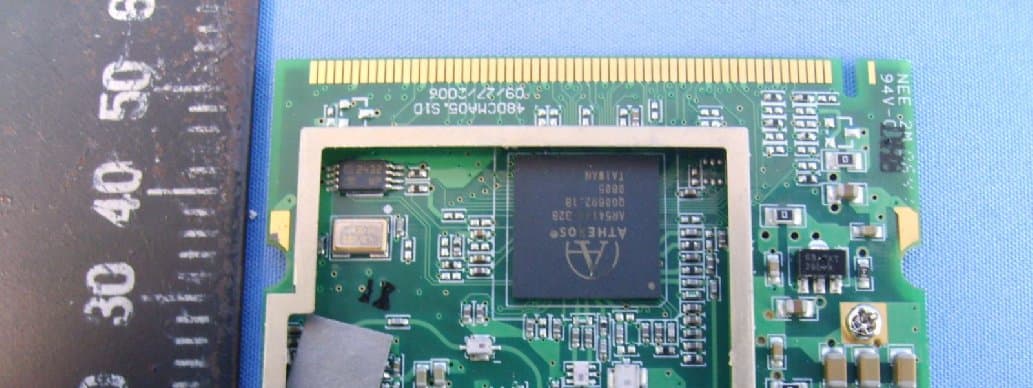
Click to zoom
Application Details
- Equipment Class
- DTS - Digital Transmission System
- Date of Grant
- Feb 26, 2007
- Application Purpose
- Original Equipment
- Date of Application
- Feb 26, 2007
- Equipment Note
- High Powered 802.11a/g WLAN Mini-PCI 3A
- Frequency Range
- 5745.00000000 - 5825.00000000
- Company
- Wistron NeWeb Corporation
- Country
- Taiwan
Documents & Files
Document Text
Text extracted from the exhibit documents filed with the FCC. Open a document above to read the original.
Users Manual
WLAN 802.11a/b/g mini-PCI Module User Manual (DCMA-82) Version: 1.0 Nov. 2006 1 Copyright Statement No part of this publication may be reproduced, stored in a retrieval system, or transmitted in any form or by any means, whether electronic, mechanical, photocopying, recording or otherwise without the prior writing of the publisher. Windows ™ 98SE/2000/ME/XP are trademarks of Microsoft ® Corp. Pentium is trademark of Intel. All copyright reserved. 2 DCMA-82 Compliances Federal Communication Commission Interference Statement This equipment has been tested and found to comply with the limits for a Class B digital device, pursuant to Part 15 of the FCC Rules. These limits are designed to provide reasonable protection against harmful interference in a residential installation. This equipment generates, uses and can radiate radio frequency energy and, if not installed and used in accordance with the instructions, may cause harmful interference to radio communications. However, there is no guarantee that interference will not occur in a particular installation. If this equipment does cause harmful interference to radio or television reception, which can be determined by turning the equipment off and on, the user is encouraged to try to correct the interference by one of the following measures: Reorient or relocate the receiving antenna Increase the separation between the equipment and receiver Connect the equipment into an outlet on a circuit different from that to which the receiver is connected Consult the dealer or an experienced radio/TV technician for help FCC Caution: Any changes or modifications not expressly approved by the party responsible for compliance could void the users authority to operate this equipment. This device complies with Part15 of the FCC Rules. Operation is subject to the following two conditions: (1) This device may not cause harmful interference, and (2) This device must accept any interference received, including interference that may cause undesired operation. IEEE 802.11 b or 802.11 g operation of this product in the U.S.A. is firmware‐limited to channels 1 through 11. IMPORTANT NOTE: FCC Radiation Exposure Statement: This equipment complies with FCC radiation exposure limits set forth for an uncontrolled environment. This equipment should be installed and operated with minimum distance 20cm between the radiator & your body. This transmitter must not be co‐located or operating in conjunction with any other antenna or transmitter. The availability of some specific channels and/or operational frequency bands is country dependent and is firmware programmed at the factory to match the intended destination. The firmware setting is not accessible by the end user. Wireless 5 GHz Band Statements: As the Access Point can operate in the 5150‐5250 MHz frequency band it is limited by the FCC to indoor use only so as to reduce the potential for harmful interference to co‐channel Mobile Satellite systems. High power radars are allocated as primary users (meaning they have priority) of the 5250‐5350 MHz 3 and 5650‐5850 MHz bands. These radars could cause interference and /or damage to the access point when used in Canada. Wireless 4.9 GHz Band Statements: (please refer to Appendix B for detailed limitation) Installation and operation requires an approved license from the FCC. This device is intended only for OEM integrators under the following conditions: 1) The antenna must be installed such that 20 cm is maintained between the antenna and users, and 2) The transmitter module may not be co‐located with any other transmitter or antenna, 3) For all products market in US, OEM has to limit the operation channels in CH1 to CH11 for 2.4G bands by supplied firmware programming tool. OEM shall not supply any tool or info to the end‐user regarding to Regulatory Domain change. 4) Due to the involvement of FCC part 90(Y) 4.9G safety band operation, the end product must be professional installed and can not be marketed to the general public. As long as 4 conditions above are met, further transmitter test will not be required. However, the OEM integrator is still responsible for testing their end‐product for any additional compliance requirements required with this module installed (for example, digital device emissions, PC peripheral requirements, etc.). IMPORTANT NOTE: In the event that these conditions can not be met (for example certain laptop configurations or co‐location with another transmitter), then the FCC authorization is no longer considered valid and the FCC ID can not be used on the final product. In these circumstances, the OEM integrator will be responsible for re‐evaluating the end product (including the transmitter) and obtaining a separate FCC authorization. End Product Labeling This transmitter module is authorized only for use in device where the antenna may be installed such that 20 cm may be maintained between the antenna and users. The final end product must be labeled in a visible area with the following: “Contains FCC ID: NKRDCMA82”. Manual Information To the End User The OEM integrator has to be aware not to provide information to the end user regarding how to install or remove this RF module in the user’s manual of the end product that integrates this module. The end user manual shall include all required regulatory information/warning as show in this manual. 4 5 Table of Contents 1. INTRODUCTION 6 1.1 SYSTEM REQUIREMENTS.........................................................................................6 1.2 FEATURES.................................................................................................................6 2. DRIVER/UTILITY INSTALLATION / UNINSTALLATION 7 2.1 INSTALLATION..........................................................................................................7 2.2 ADDITIONAL SETUP PROCESSES............................................................................10 2.3 UNINSTALLATION................................…
Text truncated - open the document above for the full version.
Cover Letter(s)
FCC ID: NKRDCMA82 Report No. RF951124L01 Modular Approval Request Letter Advance Data Technology Feb. 08, 2007 Dear Application Examiner, Wistron NeWeb Corp.’s High Powered 802.11a/g WLAN Mini-PCI 3A, FCC ID: NKRDCMA82, would like to have your authorization as a modular approval. The requirements of Public Notice DA00-1407 have been met and shown on the following statements. 1. “The modular transmitter must have its own RF shielding.” The radio portion of this module has been shielded, please see exhibition External Photo. 2. “The modular transmitter must have buffered modulation/data inputs.” The EUT has buffered data inputs, it is integrated in chip AR5414A. 3. “The modular transmitter must have its own power supply regulation.” The chips RF converter which will influence the frequency radiation, have to be 1.8VDC powered. The PCMCIA interface provides 3.3VDC, so there are regulators in front of these chips, the part number of this regulator is RT9266PE. 4. “The modular transmitter must comply with the antenna requirements of section 15.203 and 15.204(C).” The EUT meets the FCC antenna requirements. The spurious emission, unique antenna connector and photo of antennas are shown in the test report. 5. “The modular transmitter must be tested in a stand-alone configuration” The EUT was placed on an extended card which connected to Notebook Computer as a stand-alone configuration. The EUT was tested via the outside a Notebook Computer. Please see section Photographs of Test Configuration in the test report. 6. “The modular transmitter must be labeled with its own FCC ID number.” Please see exhibition Label Sample for the FCC ID of this module. And also in the exhibition Users Manual, there are instructions give to the OEM on how to label the end product. FCC ID: NKRDCMA82 Report No. RF951124L01 7. “The modular transmitter must comply with any specific rule or operating requirements applicable to the transmitter and the manufacturer must provide adequate instructions along with the module to explain any such requirements.” The EUT is compliant with all applicable FCC rules. Detail instructions for maintaining compliance are given in the Users Manual. 8. “The modular transmitter must comply with any applicable RF exposure requirements.” The EUT is compliant with all applicable RF exposure requirements. RF Exposure is addressed in the RF exposure exhibition. Please contact me if you have any further questions. Thanks for your attention. Best Regards, Eric Lin Manager of Hsinchu Certification Service Div. Advance Data Technology
External Photos
Page 1 CONSTRUCTION PHOTOS OF EUT EUT Sample for MMCX connector Page 2 EUT Sample for U.FL connector
ID Label/Location Info
FCC ID: NKRDCMA82 FCC LABEL LOCATION The label will be permanently affixed at a conspicuous location on the device. Label
ID Label/Location Info
Product Code: DCMA-82DCMA-82 High Powered 802.11a/g WLAN Mini-PCI 3A, U. FL Ordering P/N: Input: DC 3.3V, 880 mA FCC ID: NKRDCMA82 Made in Taiwan MAC: 000B8B1D75643S/N: 000B8B1D75643
Internal Photos
Page 1 CONSTRUCTION PHOTOS OF EUT EUT Sample for MMCX connector Page 2 Page 3 EUT Sample for U.FL connector Page 4 Page 5 Antenna Model No.: DBA-SSMA-01 Page 6 Antenna Model No.: SRSM2400MRA Page 7
Internal Photos
Page 8 Page 9 Page 10 Antenna Model No.: SRSM5150MRA Page 11 Page 12 Antenna Model No.: SPA 5500/40/14/O/V_C Page 13 Page 14
Operational Description
FCC ID: NKRDCMA82 Report No. 9511124L01 Technical Description This device is a High Powered 802.11a/g WLAN Mini-PCI 3A operates in 4.9GHz and both the 5GHz and 2.4GHz Bands with DSSS and OFDM technique. The transmitter rate could be 1/2/5.5/6/9/11/12/18/24/ 36/48/54Mbps (Turbo mode: up to 108Mbps). The transmitter of the EUT is powered from host equipment. The antennas are as following: For 2.4GHz No. Brand Name Model No. Gain (dBi) Cable Loss (dB) Net Gain (dB) Antenna Type Connector 1 * Wistron Neweb Corp. DBA-SSMA-01 1.29 0.5 0.79 dipole RSMA 2 CUSHCRUFT SRSM2400MRA 2 0.5 1.5 dipole RSMA Note: For 2.4GHz antennas, antenna 2 was selected as representative antenna for the test. For 5GHz No. Brand Name Model No. Gain (dBi) Cable Loss (dB) Net Gain (dB) Antenna Type Connector A * Wistron Neweb Corp. DBA-SSMA-01 2.06 0.9 1.16 dipole RSMA B CUSHCRUFT SRSM5150MRA 2 0.9 1.1 dipole RSMA C ** HUBER+ SUHNER SPA 5500/40/14/O/V_C 13.5 0.9 12.6 panel SMA Note: 1. For 5GHz antennas, antenna A and C were selected as representative antennas for the test. 1. “*’” is a Dual Band antenna can be used in both 2.4GHz and 5GHz. 2. “**’” is an Outdoor Antenna it can only be used in point-to-point applications. Under normal use condition, the user has to keep at least 20 cm separation distance between radiator and the body of the user. 11abg could not simultaneously transmit with 90Y. For more detailed instruction, please refer to the user’s manual. FCC ID: NKRDCMA82 Report No. 9511124L01 FCC 15.407(c) states : The device shall automatically discontinue transmission in case of either absence of information to transmit or operational failure. These provisions are not intended to preclude the transmission of control or signaling information or the use of repetitive codes used by certain digital technologies to complete frame or burst intervals. Applicants shall include in their application for equipment authorization a description of hoe this requirement is met. Data transmission is always initiated by software, which is then pass down through the MAC, through the digital and analog baseband, and finally to the RF chip. Several special packets (ACKs, CTS, PSPoll, etc...) are initiated by the MAC. There are the only ways the digital baseband portion will turn on the RF transmitter, which it then turns off at the end of the packet. Therefore, the transmitter will be on only while one of the aforementioned packets are being transmitted.
Parts List/Tune Up Info
WNC's DCMA-82 MMCX BOM Item Description Quantity Reference Designator Vendor Vendor Part Number 1 CAP,0402,NPO,0.3pF,+/- 0.1pF, 50V 1 C48(C2) Tayi yuden EVK105CH0R3BW 2 CAP,0402,NPO,0.4pF,+/- 0.1pF, 50V 1 C41(C2) Darfon C1005NP0408BGT 3 CAP,0402,NPO,0.5pF,+/- 0.1pF, 50V 4 C11(B2),C15(B2),C16(B2),C39(B1) Murata GRM1555C1HR50BZ01E 4 CAP,0402,NPO,1pF,+/- 0.25pF,50V 6 C17(A3),C21(B2),C51(C1),C59(C1),C42(C1),C43(C1) Murata GRM1555C1H1R0CZ01E 5 !CAP 1.5P GRM1555C1H1R5BZ01D 1 Ca6(C1) Murata GRM1555C1H1R5BZ01E 6 CAP,0402,NPO,1.8pF,+/- 0.25pF,50V 3 C2(B2),L8(B3),C12(B2) PHYCOMP 2238-869-15188 7 CAP,0402,NPO,2.0pF,+/- 0.25pF, 50V 1 C38(B1) Murata GRM1555C1H2R0CZ01D 8 CAP,0402,NPO,2.2pF,+/- 0.25pF, 50V 3 C9(B2),C46(C2),C3(A3) PHYCOMP 2238-869-15228 9 !CHIP CAP 8.2P GRM1555C1H8R2D 4 C52(B1),C53(C1),C60(C1),C47(C1) MURATA GRM1555C1H8R2CZ01D 10 CAP,0402,NPO,10pF, +/- 5%, 50V 12 C4(A3),C18(B2),C19(B2),C23(B2),C67(B2),C84(B2),C103(B2),C105(B2),C118(B2),C119(B2),C27(C2),C80(A1), Murata GRM1555C1H100JZ01E 11 CAP,0402,NPO,15pF, +/- 2%, 50V 2 C25(C2),Ca7(C1) Darfon C1005NPO150GGT 12 CAP,0402,NPO,18pF,+/- 2%, 50V 1 C117(C3), Darfon C1005NP0180GGT 13 !*CHIP CAP 33pF 50V J 0402 1 C34(C1),Ca4(B1) Darfon C1005NPO330JGT 14 !CHIP CAP 47pF 50V J 0402 1 C30(C2), Murata GRM1555C1H470JZ01D 15 CAP,0402,NPO,120pF,+/- 5%, 50V 1 C22(B2), PHYCOMP 2238-869-15121 16 CAP,0402,NPO,100pF,+/- 5%, 50V 2 C32(C2),C26(C2), Murata GRM1555C1H101JD01D 17 *!CHIP CAP C 1000P 50V K0402 5 C55(B1), C63(B1),Ca2(B2),C28(C2),C10(B1) Darfon C1005X7R102KGT 18 CAP,0603,X7R,22nF,50V 3 C82(A2),C95(A3),C96(A2) Murata GRM188R71H223KA01D 19 CAP,0402,X5R,0.1uF,+/- 10%, 10V 10 C72(B2),C73(B3),C54(B1),C50(B1),C75(B3),C93(B3), C98(B2),C37(B2),C56(B1),C14(A1) Murata GRP155R61A104KA01E 20 !CHIP CAP 1uF 16V K 0603 X5R 1 C78(A1) Murata GRM188R61C105KA12D 21 !CHIP CAP 1UF 6.3V K0402 X5R 6 C5(A1),C79(A1).C36(C2),C29(C2), Ca3(C1),Ca5(B1) Murata GRM155R60J105KE19D 22 CAP,0805,X5R,2.2uF, +/- 10%, 10V 2 C89(A2),C71(A3) TAIYO_YUDEN CELMK212BJ225KG-T WNC's DCMA-82 MMCX BOM Item Description Quantity Reference Designator Vendor Vendor Part Number 23 !CHIP CAP 4.7UF 6.3V 0603 X5R 1 C24(B1) Murata GRM188R60J475KE19D 24 !CHIP CAP 10UF 6.3V +- 20% 0603 X5R 3 C99(C2),C100(B1),C31(C2) Murata GRM188R60J106M 25 CHIP CAP 47UF M1206 6.3V X5R 5 C69(A2),C70(A1),C77(A2),C81(A1),C35(A2),C33(A1) 1. Murata 2.Taiyo yuden 1. GRM31CR60J476M 2.JMK316BJ476ML-T 26 ! Schottky Diode M1FH3 1 D2(A1) Shindengen M1FH3 27 LFB2H2G45SG7B734,BAND PASS FILTER,2GHz 1 Fa2(B2) Murata LFB2H2G45SG7B734 28 RF_SPEC,BALUN,5GHz 1 F1(B2) Murata LDB215G5110C-001 29 DIPLEXER,SMD,6PIN 1 F4(C1), ACX DP2012-E2455DAT/LF 30 DIPLEXER,SMD,6PIN 1 Fa3(B1) NTK LDTOUQD-3060E 31 RF_SPEC,BAND PASS FILTER,5GHz 1 F7(B2) Murata LFB215G37SG8A185 32 SMT MMCX CONN 2 J2(C1),J3(B1) Inputoutput M109-700A 33 !IND,0402,1.5nH,+/- 0.1nH 1 L7(B2) CYNTEC CML0510-1N5-BN 34 IND,0402,2.7nH,+/- 0.1nH 2 C13(B2),L3(C1) CYNTEC CML0510-2N7-BN 35 CHIP IND 2.7NH S 0402 2 La2(C1),La3(B1) Darfon HI10052N7ST 36 *CHIP IND 3.3NH S 0402 DARFON 3 L1(C2),L4(C2),L10(B1) Darfon HI10053N3ST 37 !IND,0402,4.3nH,+/- 0.1nH 1 L5(B1) Viking AL02BT4N3M 38 !Power CHOKE 8.2uH GSSR53P-8R2M 1 L2(A1) Gotrend GSSR53P-8R2M 39 ! CHIP RES 0 J 1/8W 0805 3 L13(A3),R24(A3),R59(A2), YAGEO RC0805JR-070R 40 TRA, SOT-89, PNP General Purpose Amplifier 1 Q3(A2) CENTRAL SEMI CXT2907ATR 41 !N-MOS 4A AP2306GN 1 Q5(A1) Advanced Power AP2306GN 42 CHIP RES 0 J 1/16W 0402 2 R4(A3),R11(A3), 大毅 (TA-I) RM04JT0R0 43 ! CHIP RES 0 J 1/4W 1206 1 R25(A1) YAGEO RC1206JR-070RL 44 RES,0603,1 OHM, 5%, 1/10W 1 R40(A2) YAGEO RC0402 45 !CHIP RES 10 J 1/16W 0402 2 R67(C2),R68(C2) TA-I RM04JTN100 46 !CHIP RES 1M F 1/16W 0402 1 R61(A1) Yageo RC0402FR-071M 47 !CHIP RES 110 J 1/16W 0402 1 R46(C2) Yageo RC0402JR-07110R 48 !!CHIP RES 10K F1/16W 0402(TA- 4 R1(A3),R15(C3),R17(C3),R69(C2) TA-I RM04FTN1002 WNC's DCMA-82 MMCX BOM Item Description Quantity Reference Designator Vendor Vendor Part Number 49 RES,0402,1.1K OHMS, +/- 1%, 1/16W 2 R18(C2),R63(C2), 1. YAGEO 2.TA-I 1. RC0402FR-071K1L 2.RM04FTN1101 50 RES,0402,1.2K OHMS, +/- 5%, 1/16W 1 Rb2(B2) Yageo RC0402JR-071K2 51 !CHIP RES 187 F 1/16W 0402 2 R2(A3),R6(A3) TA-I RM04FTN1870 52 !CHIP RES 16.9 F 1/16W 0402 2 R70(B2),R49(B2) Yageo RC0402FR-0716R9L 53 !CHIP RES 2.2K J 1/16W 0402 1 Rb5(B2) TA-I RM04JTN222 54 !CHIP RES 2.7K F 1/16W 0402 1 Rb7(B2) TA-I RM04FTN2701 55 !CHIP RES 24K J 1/16W 0402 Rb6(C2) TA-I RM04JTN243 56 !CHIP RES 300 OHMS 1/16W F0402 5 Rb4(B2),R71(B2),R72(B1),Rb3(B2), Rb1(B2) Yageo RC0402FR-07300RL 57 !CHIP RES 3K OHMS 1/16W J0402 1 R52(B1) TA-I RM04JTN302 58 !CHIP RES 3M F 1/16W 0402 1 R62(A1) Yageo RC0402FR-073ML 59 !CHIP RES 43K 1/16W J0402 (YAG 1 R41(B2) YAGEO RC0402JR-0743KL 60 ! CHIP RES 47 J 1/16W 0402 3 R31(B2),R35(B2),R36(B2) TA-I 1.RM04JTN470 61 !CHIP RES 499 F 1/16W 0402 1 R48(C2) YAGEO RC0402FR-07499R 62 ! CHIP RES 4.7K J 1/16W 0402 1 Ra1(B1) TA-I RM04JTN472 63 !CHIP RES 47K J 1/16W 0402 1 R60(A1) TA-I RM04JTN473 64 *!CHIP RES 56K J 1/16W 0402 1 R45(B2), TA-I RM04JTN563 65 !CHIP RES 60.4 F 1/16W 0402 1 R47(C2) YAGEO RC0402FR-0760R4 66 CHIP RES 6.19K F 1/16W 0402 1 R42(B2) YAGEO RC0402FR-076K19L 67 RF_SPEC,SWI,DPDT Diversity 1 S1(C1) Hexawave HWS415 68 AR5414A-B2B, BGA, A/B/G, ANALOG AND DIGITAL 1 U1(B2) ATHEROS AR5414A-B2B 69 ! Setp up DC/DC convertor RT9266PE 1 U2(A1) Richtek RT9266PE 70 IC,TSSOP8,Serial 32Kbit EEPROM 1 U3(C3) ST MICROELECTRONICS M24C32WDW 71 802.11 MMIC LNA XM2458LA-BL1301 1 U4(B1) Murata XM2458LA-BL1301 72 5GHz MMIC PA LX5530 1 U6(C2) Microsemi LX5530-LQTR 73 2.4Ghz PA RFIC AP1046 1 U7(B1) RFIC AP1046 WNC's DCMA-82 MMCX BOM Item Description Quantity Reference Designator Vendor Vendor Part Number 74 40MHZ XTAL FY4000015 -40~85 DEGREES C 1 Y1(C2) eCERA FY4000015 75 Shileding Cover 1 location : C1 76 3.2mm shiedling frame 1 location : C1 77 screw 2 7879 heat sink 1 5IC 1 U5(A3)
Parts List/Tune Up Info
WNC's DCMA-82 U.FL BOM Item Description Quantity Reference Designator Vendor Vendor Part Number 1 CAP,0402,NPO,0.3pF,+/- 0.1pF, 50V 1 C48(C2) Tayi yuden EVK105CH0R3BW 2 CAP,0402,NPO,0.4pF,+/- 0.1pF, 50V 1 C41(C2) Darfon C1005NP0408BGT 3 CAP,0402,NPO,0.5pF,+/- 0.1pF, 50V 4 C11(B2),C15(B2),C16(B2),C39(B1) Murata GRM1555C1HR50BZ01E 4 CAP,0402,NPO,1pF,+/- 0.25pF,50V 6 C17(A3),C21(B2),C51(C1),C59(C1),C42(C1),C43(C1) Murata GRM1555C1H1R0CZ01E 5 !CAP 1.5P GRM1555C1H1R5BZ01D 1 Ca6(C1) Murata GRM1555C1H1R5BZ01E 6 CAP,0402,NPO,1.8pF,+/- 0.25pF,50V 3 C2(B2),L8(B3),C12(B2) PHYCOMP 2238-869-15188 7 CAP,0402,NPO,2.0pF,+/- 0.25pF, 50V 1 C38(B1) Murata GRM1555C1H2R0CZ01D 8 CAP,0402,NPO,2.2pF,+/- 0.25pF, 50V 3 C9(B2),C46(C2),C3(A3) PHYCOMP 2238-869-15228 9 !CHIP CAP 8.2P GRM1555C1H8R2D 4 C52(B1),C53(C1),C60(C1),C47(C1) MURATA GRM1555C1H8R2CZ01D 10 CAP,0402,NPO,10pF, +/- 5%, 50V 12 C4(A3),C18(B2),C19(B2),C23(B2),C67(B2),C84(B2),C103(B2),C105(B2),C118(B2),C119(B2),C27(C2),C80(A1), Murata GRM1555C1H100JZ01E 11 CAP,0402,NPO,15pF, +/- 2%, 50V 2 C25(C2),Ca7(C1) Darfon C1005NPO150GGT 12 CAP,0402,NPO,18pF,+/- 2%, 50V 1 C117(C3), Darfon C1005NP0180GGT 13 !*CHIP CAP 33pF 50V J 0402 1 C34(C1),Ca4(B1) Darfon C1005NPO330JGT 14 !CHIP CAP 47pF 50V J 0402 1 C30(C2), Murata GRM1555C1H470JZ01D 15 CAP,0402,NPO,120pF,+/- 5%, 50V 1 C22(B2), PHYCOMP 2238-869-15121 16 CAP,0402,NPO,100pF,+/- 5%, 50V 2 C32(C2),C26(C2), Murata GRM1555C1H101JD01D 17 *!CHIP CAP C 1000P 50V K0402 5 C55(B1), C63(B1),Ca2(B2),C28(C2),C10(B1) Darfon C1005X7R102KGT 18 CAP,0603,X7R,22nF,50V 3 C82(A2),C95(A3),C96(A2) Murata GRM188R71H223KA01D 19 CAP,0402,X5R,0.1uF,+/- 10%, 10V 10 C72(B2),C73(B3),C54(B1),C50(B1),C75(B3),C93(B3), C98(B2),C37(B2),C56(B1),C14(A1) Murata GRP155R61A104KA01E 20 !CHIP CAP 1uF 16V K 0603 X5R 1 C78(A1) Murata GRM188R61C105KA12D 21 !CHIP CAP 1UF 6.3V K0402 X5R 6 C5(A1),C79(A1).C36(C2),C29(C2), Ca3(C1),Ca5(B1) Murata GRM155R60J105KE19D 22 CAP,0805,X5R,2.2uF, +/- 10%, 10V 2 C89(A2),C71(A3) TAIYO_YUDEN CELMK212BJ225KG-T WNC's DCMA-82 U.FL BOM WNC's DCMA-82 U.FL BOM Item Description Quantity Reference Designator Vendor Vendor Part Number 23 !CHIP CAP 4.7UF 6.3V 0603 X5R 1 C24(B1) Murata GRM188R60J475KE19D 24 !CHIP CAP 10UF 6.3V +- 20% 0603 X5R 3 C99(C2),C100(B1),C31(C2) Murata GRM188R60J106M 25 CHIP CAP 47UF M1206 6.3V X5R 5 C69(A2),C70(A1),C77(A2),C81(A1),C35(A2),C33(A1) 1. Murata 2.Taiyo yuden 1. GRM31CR60J476M 2.JMK316BJ476ML-T 26 ! Schottky Diode M1FH3 1 D2(A1) Shindengen M1FH3 27 LFB2H2G45SG7B734,BAND PASS FILTER,2GHz 1 Fa2(B2) Murata LFB2H2G45SG7B734 28 RF_SPEC,BALUN,5GHz 1 F1(B2) Murata LDB215G5110C-001 29 DIPLEXER,SMD,6PIN 1 F4(C1), ACX DP2012-E2455DAT/LF 30 DIPLEXER,SMD,6PIN 1 Fa3(B1) NTK LDTOUQD-3060E 31 RF_SPEC,BAND PASS FILTER,5GHz 1 F7(B2) Murata LFB215G37SG8A185 32 CON,Ultra-Miniature Coax 2 J2(C1),J3(B1) HRS U.FL-SMT(10)RSB-I 33 !IND,0402,1.5nH,+/- 0.1nH 1 L7(B2) CYNTEC CML0510-1N5-BN 34 IND,0402,2.7nH,+/- 0.1nH 2 C13(B2),L3(C1) CYNTEC CML0510-2N7-BN 35 CHIP IND 2.7NH S 0402 2 La2(C1),La3(B1) Darfon HI10052N7ST 36 *CHIP IND 3.3NH S 0402 DARFON 3 L1(C2),L4(C2),L10(B1) Darfon HI10053N3ST 37 !IND,0402,4.3nH,+/- 0.1nH 1 L5(B1) Viking AL02BT4N3M 38 !Power CHOKE 8.2uH GSSR53P-8R2M 1 L2(A1) Gotrend GSSR53P-8R2M 39 ! CHIP RES 0 J 1/8W 0805 3 L13(A3),R24(A3),R59(A2), YAGEO RC0805JR-070R 40 TRA, SOT-89, PNP General Purpose Amplifier 1 Q3(A2) CENTRAL SEMI CXT2907ATR 41 !N-MOS 4A AP2306GN 1 Q5(A1) Advanced Power AP2306GN 42 CHIP RES 0 J 1/16W 0402 2 R4(A3),R11(A3), 大毅 (TA-I) RM04JT0R0 43 ! CHIP RES 0 J 1/4W 1206 1 R25(A1) YAGEO RC1206JR-070RL 44 RES,0603,1 OHM, 5%, 1/10W 1 R40(A2) YAGEO RC0402 45 !CHIP RES 10 J 1/16W 0402 2 R67(C2),R68(C2) TA-I RM04JTN100 46 !CHIP RES 1M F 1/16W 0402 1 R61(A1) Yageo RC0402FR-071M 47 !CHIP RES 110 J 1/16W 0402 1 R46(C2) Yageo RC0402JR-07110R 48 !!CHIP RES 10K F1/16W 0402(TA- 4 R1(A3),R15(C3),R17(C3),R69(C2) TA-I RM04FTN1002 WNC's DCMA-82 U.FL BOM WNC's DCMA-82 U.FL BOM Item Description Quantity Reference Designator Vendor Vendor Part Number 49 RES,0402,1.1K OHMS, +/- 1%, 1/16W 2 R18(C2),R63(C2), 1. YAGEO 2.TA-I 1. RC0402FR-071K1L 2.RM04FTN1101 50 RES,0402,1.2K OHMS, +/- 5%, 1/16W 1 Rb2(B2) Yageo RC0402JR-071K2 51 !CHIP RES 187 F 1/16W 0402 2 R2(A3),R6(A3) TA-I RM04FTN1870 52 !CHIP RES 16.9 F 1/16W 0402 2 R70(B2),R49(B2) Yageo RC0402FR-0716R9L 53 !CHIP RES 2.2K J 1/16W 0402 1 Rb5(B2) TA-I RM04JTN222 54 !CHIP RES 2.7K F 1/16W 0402 1 Rb7(B2) TA-I RM04FTN2701 55 !CHIP RES 24K J 1/16W 0402 Rb6(C2) TA-I RM04JTN243 56 !CHIP RES 300 OHMS 1/16W F0402 5 Rb4(B2),R71(B2),R72(B1),Rb3(B2), Rb1(B2) Yageo RC0402FR-07300RL 57 !CHIP RES 3K OHMS 1/16W J0402 1 R52(B1) TA-I RM04JTN302 58 !CHIP RES 3M F 1/16W 0402 1 R62(A1) Yageo RC0402FR-073ML 59 !CHIP RES 43K 1/16W J0402 (YAG 1 R41(B2) YAGEO RC0402JR-0743KL 60 ! CHIP RES 47 J 1/16W 0402 3 R31(B2),R35(B2),R36(B2) TA-I 1.RM04JTN470 61 !CHIP RES 499 F 1/16W 0402 1 R48(C2) YAGEO RC0402FR-07499R 62 ! CHIP RES 4.7K J 1/16W 0402 1 Ra1(B1) TA-I RM04JTN472 63 !CHIP RES 47K J 1/16W 0402 1 R60(A1) TA-I RM04JTN473 64 *!CHIP RES 56K J 1/16W 0402 1 R45(B2), TA-I RM04JTN563 65 !CHIP RES 60.4 F 1/16W 0402 1 R47(C2) YAGEO RC0402FR-0760R4 66 CHIP RES 6.19K F 1/16W 0402 1 R42(B2) YAGEO RC0402FR-076K19L 67 RF_SPEC,SWI,DPDT Diversity 1 S1(C1) Hexawave HWS415 68 AR5414A-B2B, BGA, A/B/G, ANALOG AND DIGITAL 1 U1(B2) ATHEROS AR5414A-B2B 69 ! Setp up DC/DC convertor RT9266PE 1 U2(A1) Richtek RT9266PE 70 IC,TSSOP8,Serial 32Kbit EEPROM 1 U3(C3) ST MICROELECTRONICS M24C32WDW 71 802.11 MMIC LNA XM2458LA-BL1301 1 U4(B1) Murata XM2458LA-BL1301 72 5GHz MMIC PA LX5530 1 U6(C2) Microsemi LX5530-LQTR 73 2.4Ghz PA RFIC AP1046 1 U7(B1) RFIC AP1046 WNC's DCMA-82 U.FL BOM WNC's DCMA-82 U.FL BOM Item Description Quantity Reference Designator Vendor Vendor Part Number 74 40MHZ XTAL FY4000015 -40~85 DEGREES C 1 Y1(C2) eCERA FY4000015 75 Shileding Cover 1 location : C1 76 3.2mm shiedling frame 1 location : C1 77 screw 2 #REF! ! Absorber BN-006-050.008.008 1 location : C2 錩潤科技 BN-006-050.008.008 #REF! heat sink 1 WN…
Text truncated - open the document above for the full version.
RF Exposure Info
Report No.: SA951124L01 1 Issued: Jan. 22, 2007 RF EXPOSURE REPORT REPORT NO.: SA951124L01 MODEL NO.: DCMA-82, DCMA-82 High Power, DCMA-IHP, DCMA-HP, CM11, CM10-HI, CM10-H, DCMA-SPI FCC ID: NKRDCMA82 ACCORDING: FCC Guidelines for Human Exposure IEEE C95.1 APPLICANT: Wistron NeWeb Corp. ADDRESS: No. 10-1, Li-hsin Road I, Hsinchu Science Park, Hsinchu 300, Taiwan, R.O.C. ISSUED BY: Advance Data Technology Corporation LAB LOCATION: No. 81-1, Lu Liao Keng, 9 Ling, Wu Lung Tsuen, Chiung Lin Hsiang, Hsin Chu Hsien, Taiwan, R.O.C. Report No.: SA951124L01 2 Issued: Jan. 22, 2007 RF Exposure Measurement 1. Introduction In this document, we try to prove the safety of radiation harmfulness to the human body for our product. The limit for Maximum Permissible Exposure (MPE) specified in FCC 1.1310 is followed. The Gain of the antenna used in this product is measured in a Fully Anechoic Chamber (FAC) calibrated for antenna measurement in ADT, and also the maximum total power input to the antenna is measured. Through the Friis transmission formula and the maximum gain of the antenna, we can calculate the distance, away from the product, where the limit of MPE is reached. Although the Friis transmission formula is a far field assumption, the calculated result of that is an over-prediction for near field power density. We will take that as the worst case to specify the safety range. 2. RF Exposure Limit According to FCC 1.1310: The criteria listed in the following table shall be used to evaluate the environmental impact of human exposure to radio-frequency (RF) radiation as specified in 1.1307(b) LIMITS FOR MAXIMUM PERMISSIBLE EXPOSURE (MPE) Frequency Range (MHz) Electric Field Strength (V/m) Magnetic Field Strength (A/m) Power Density (mW/cm 2 ) Average Time (minutes) (A)Limits For Occupational / Control Exposures 300-1500 ... ... F/300 6 1500-100,000 ... ... 5 6 (B)Limits For General Population / Uncontrolled Exposure 300-1500 ... ... F/1500 6 1500-100,000 ... ... 1.0 30 F = Frequency in MHz Report No.: SA951124L01 3 Issued: Jan. 22, 2007 3. Friis Formula Friis transmission formula : Pd = (Pout*G) / (4*pi*r 2 ) where Pd = power density in mW/cm 2 Pout = output power to antenna in mW G = gain of antenna in linear scale Pi = 3.1416 R = distance between observation point and center of the radiator in cm Pd is the limit of MPE, 1 mW/cm 2 . If we know the maximum Gain of the antenna and the total power input to the antenna, through the calculation, we will know the MPE value at distance 20cm. Ref. : David K. Cheng, Field and Wave Electromagnetics, Second Edition, Page 640, Eq. (11-133). 4 EUT Operating condition The software provided by Manufacturer enabled the EUT to transmit and receive data at lowest, middle and highest channel individually. 5. Classification The antenna of this product, under normal use condition, is at least 20cm away from the body of the user. Warning statement to the user for keeping at least 20cm or more separation distance with the antenna should be included in users manual. So, this device is classified as Mobile Device Report No.: SA951124L01 4 Issued: Jan. 22, 2007 6 Test Results 6.1 Antenna Gain For 2.4GHz No. Brand Name Model No. Gain (dBi) Cable Loss (dB) Net Gain (dB) Antenna Type Connector 1 * Wistron Neweb Corp. DBA-SSMA-01 1.29 0.5 0.79 dipole RSMA 2 CUSHCRUFT SRSM2400MRA 2 0.5 1.5 dipole RSMA Note: For 2.4GHz antennas, antenna 2 was selected as representative antenna for the test. For 4.9GHz and 5GHz No. Brand Name Model No. Gain (dBi) Cable Loss (dB) Net Gain (dB) Antenna Type Connector A * Wistron Neweb Corp. DBA-SSMA-01 2.06 0.9 1.16 dipole RSMA B CUSHCRUFT SRSM5150MRA 2 0.9 1.1 dipole RSMA C ** HUBER+ SUHNER SPA 5500/40/14/O/V_C 13.5 0.9 12.6 panel SMA Note: 1. For 5GHz antennas, antenna A and C were selected as representative antennas for the test. 1. “*’” is a Dual Band antenna can be used in both 2.4GHz and 5GHz. 2. “**’” is an Outdoor Antenna it can only be used in point-to-point applications. Report No.: SA951124L01 5 Issued: Jan. 22, 2007 6.2 Output Power Into Antenna & RF Exposure value: For 2.4GHz 802.11b: Antenna 2 Channel Channel Frequency (MHz) Output Power to Antenna (mW) Power Density (mW/cm 2 ) Limit of Power Density (mW/cm 2 ) 1 2412 70.795 0.020 1.0 6 2437 234.423 0.066 1.0 11 2462 223.872 0.063 1.0 802.11g: Antenna 2 Channel Channel Frequency (MHz) Output Power to Antenna (mW) Power Density (mW/cm 2 ) Limit of Power Density (mW/cm 2 ) 1 2412 95.499 0.027 1.0 6 2437 363.078 0.102 1.0 11 2462 141.254 0.040 1.0 6 (Turbo) 2437 79.433 0.025 1.0 Report No.: SA951124L01 6 Issued: Jan. 22, 2007 For 5GHz Operated in 5150MHz ~ 5250MHz: (15.407) Antenna A Channel Channel Frequency (MHz) Output Power to Antenna (mW) Power Density (mW/cm 2 ) Limit of Power Density (mW/cm 2 ) 1 5180 28.314 0.00736 1.0 4 5240 27.353 0.00711 1.0 Turbo 1 5210 29.923 0.00778 1.0 Operated in 5725 ~ 5850MHz band: (15.247) Antenna A Channel Channel Frequency (MHz) Output Power to Antenna (mW) Power Density (mW/cm 2 ) Limit of Power Density (mW/cm 2 ) 1 5745 363.078 0.09435 1.0 3 5785 331.131 0.08604 1.0 5 5825 363.078 0.09435 1.0 Turbo 1 5760 380.189 0.08409 1.0 Turbo 2 5800 263.027 0.06092 1.0 Antenna C Channel Channel Frequency (MHz) Output Power to Antenna (mW) Power Density (mW/cm 2 ) Limit of Power Density (mW/cm 2 ) 1 5745 245.471 0.56873 1.0 3 5785 331.131 0.76720 1.0 5 5825 363.078 0.84122 1.0 Turbo 1 5760 380.189 0.08409 1.0 Turbo 2 5800 263.027 0.06092 1.0 Report No.: SA951124L01 7 Issued: Jan. 22, 2007 For 4.9GHz Operated in 4940 ~ 4990MHz band: (Channel Bandwidth: 20MHz) Antenna A Channel Frequency (MHz) Output Power to Antenna (mW) Power Density (mW/cm 2 ) Limit of Power Density (mW/cm 2 ) 4950 464.515 0.12071 1.0 4965 467.735 0.12154 1.0 4980 476.431 0.12380 1.0 Antenna C Channel Frequency (MHz) Output Power to Antenna (mW) Power Density (mW/cm 2 ) Limit of Power Density (mW/cm 2 ) 4950 464.515 0.95920 1.0 4965 467.735 0.96585 1.0 4980 476.431 0.98381 1.0 Operated in 4940 ~…
Text truncated - open the document above for the full version.
Test Report
Report No.: RF951124L01 1 Report Format Version 2.0.5 FCC TEST REPORT REPORT NO.: RF951124L01 MODEL NO.: DCMA-82, DCMA-82 High Power, DCMA-IHP, DCMA-HP, CM11, CM10-HI, CM10-H, DCMA-SPI RECEIVED: Nov. 24, 2006 TESTED: Dec. 27, 2006 to Jan. 18, 2007 ISSUED: Jan. 22, 2007 APPLICANT: Wistron NeWeb Corp. ADDRESS: No. 10-1, Li-hsin Road I, Hsinchu Science Park, Hsinchu 300, Taiwan, R.O.C. ISSUED BY: Advanc…
Text truncated - open the document above for the full version.
Contact Information
Applicant
William Su(Senior Director / System Engineering dept.)
Technical Contact
Advance Data Technology Corporation (Hsin Chu)Eric Lin
[email protected]886-3-593-5343
81-1 Luliaoken, 9th Lin, Wulung Tsuen Chiunglin · Hsinchu · Taiwan
Non-Technical Contact
Advance Data Technology CorporationEric Lin
[email protected]886-3-593-5343
Test Firm
Bureau Veritas CPS (H.K.) Ltd. Taoyuan BranchRichard Chen
Technical Specifications
| # | Rule Parts | Frequency Range | Power Output |
|---|---|---|---|
| 2 | 15C | 5.75 GHz - 5.83 GHz | 380.00 mW |
Other Applications from Wistron NeWeb Corporation
NKR-ATTCGW453
Aug 25, 2026Enterprise product
Equipment Class
NII - Unlicensed National Information Infrastructure TXNKR-LS06B
Aug 24, 2026Touchscreen
Equipment Class
NII - Unlicensed National Information Infrastructure TXNKR-DWSZW
Aug 10, 2026Door/Window Sensor
Equipment Class
DXX - Part 15 Low Power Communication Device TransmitterNKR-TELE2
Jun 26, 2026TELE2
Equipment Class
NII - Unlicensed National Information Infrastructure TXNKR-VMC-SA525MAX
Jun 05, 2026NAD (Network Access Device)
Equipment Class
CXX - Communications Rcvr for use w/ licensed Tx and CBs