NKV802SMR bidrectional amplifier
PG Electronics Inc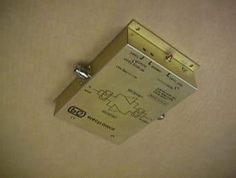
Click to zoom
Application Details
- Equipment Class
- AMP - Amplifier
- Date of Grant
- Mar 18, 2002
- Application Purpose
- Original Equipment
- Date of Application
- Jan 22, 2002
- Equipment Note
- SMR bidrectional amplifier
- Frequency Range
- 850.00000000 - 870.00000000
- Company
- PG Electronics Inc
- Country
- United States
Documents & Files
Document Text
Text extracted from the exhibit documents filed with the FCC. Open a document above to read the original.
Users Manual
P.G.TM0018AE the output signal is re-radiated and can cause interference to adjacent band users. This output power reduction is to be achieved by reduction of input power. 1-2 TABLE 1-2. Rated Power Output for Multi-tone Operation (for Intermodulation Products 50 dB down) Number ofLevel of Each Tone TonesInputOutput 1- 4.5 dBm+ 18 dBm 2- 13.5 dBm+ 9 dBm 4- 16.5 dBm+6 dBm 8- 19.5 dBm+ 3 dBm 16- 22.5 dBm0 dBm NOTE: Input level based on maximum gain limit. P.G.TM0018AE 1-3 SECTION 2. THEORY OF OPERATION 2.0 GENERAL As explained in Section 1, the A181 is a bidirectional amplifier. It provides 21 dB gain with versions available for each of the cellular, GSM, and SMR bands. The block diagram of the A181 is shown in Figure 2-1. 2.1 - The unit is composed of two band splitters or diplexers, two independent amplifiers, an alarm and voltage regulation circuit. Examine the case where the base transmit signal enters the unit via J2 (the common port of diplexer U2). The signal passes through to U2's high band output port to drive amplifier AMP 2. The output of amplifier AMP 2 is fed into the high band input of diplexer U1 and then is output at J1. 2.2 - The diplexers U1 and U2 provide isolation between the transmit and receive amplifiers. The unit's operation in the base receive band is similar to the base transmit band discussed earlier. 2.3 - The bias condition of each device in the amplifiers is monitored. If the bias changes outside certain limits a fault condition is indicated. When a fault condition occurs the standard fault reporting unit transmits the unit identification (or “Fault Code”) by two level amplitude modulation of a low frequency carrier placed on the cable center conductor. The signal is transmitted as a short burst repeated at approximately 1 to 2 minute intervals while the fault condition persists. The fault code can be programmed as described in Section 3.2. 2.4 - The voltage regulator takes 15 - 32 VDC input and provide 12 VDC output. It delivers about 250 mA during normal operation. A zener diode provides transient protection against voltage spikes on the cable. 2.5 - The bidirectional amplifier requires external DC power to be supplied through either one of the two N receptacles or from an external local power source. Internal jumpers are used to select whether DC current is drawn from J1, J2 or both. If configured to draw current from J1 or J2 then the unit will only pass RF between J1 and J2. Otherwise the unit will pass both DC and RF. When configured as a local powered unit, DC is blocked to both J1 and J2. Section 3.2 provides details on how to set up these jumpers. P.G.TM0018AE 2-1 P.G.TM0018AE Figure 2-1 A181 Bidirectional Amplifier - Block Diagram 2-2 SECTION 3. INSTALLATION, OPERATING AND MAINTENANCE INSTRUCTIONS 3.1 UNPACKING AND INSPECTION The following checks are recommended after receipt of the equipment from shipping agent: 1. Check for any external damage that could have occurred in transit. If damage is found, report to the shipping agent and to the supplier immediately. 2. Check that all items on the packing slip are present. If any are missing, report to the supplier immediately. 3.2 INSTALLATION The bidirectional amplifier is designed for mounting on a flat surface. The unit can be mounted in any orientation as desired although it is practical to select a mounting position which allows the indicators to be seen. Proceed as follows: STANDARD FAULT REPORTING UNIT: 1. Locate a suitable mounting location, allow a clearance of at least 5 inches (13 cm) to route mating cable and connectors to the unit. Drill four pilot holes on a 7.5” x 4” center for No.10 fasteners. 2. Connect J2, "BASE" to the cable leading to the base transmitter. 3. Connect J1, "ANTENNA" to the cable leading to the antenna(s). 4. If the A181 is to pass DC down the line no further action is required. Go to step 9. 5. Remove the base plate of the amplifier. 6. Locate the three removable jumpers on the PCB. These are labeled 'J1', 'DC' and 'J2'. 7. If power is drawn from J1 then remove jumper 'J2'. Go to step 9. 8. If power is drawn from J2 then remove jumper 'J1'. Go to step 9. 9. If the factory set “Fault Code” is acceptable this completed the installation. 10. If reprogramming of the fault code is required refer to Appendix A. 11. Reinstall base plate and fasten the unit to the mounting location using No.10 hardware. P.G.TM0018AE 3-1 LOCAL POWERED UNIT: 1. Locate a suitable mounting location, allow a clearance of at least 5 inches (13 cm) to route mating cable and connectors to the unit. Drill four pilot holes on a 7.5” x 4” center for No.10 fasteners. 2. Connect J2, "BASE" to the cable leading to the base transmitter. 3. Connect J1, "ANTENNA" to the cable leading to the antenna(s). 4. Connect the unit to the DC power adapter. The unit can be powered from voltages in the range 15 – 32 VDC. The connector is center positive. 3.3 OPERATING INSTRUCTIONS The A181 bidirectional amplifier has no external controls. When powered the unit will amplify signals in the transmit and receive bands. When the green light is on, current consumption of each of the active devices in the RF paths are within specifications. The red light goes on whenever (1) one or all active devices in the RF paths failed or (2) the amplifier is being driven into saturation. Corrective action for (1) is to service the amplifier and (2) is to reduce input power to the limits given in Table 1-2. P.G.TM0018AE 3-2 P.G.TM0018AE Figure 3-1. Installation Data 3-3 P.G.TM0018AE APPENDIX "A" P.G.TM0018AE FAULT CODE REPROGRAMMING If it is required to change the factory set Fault Code to the operator's custom plan then follow the following steps: 1. Remove the cover plate (ensuring that all hardware is retained). 2. Refer to the jumper field with a block of nine jumpers labeled 0 to 8 in Figure A1. 3. The code is programmable in binary with the numbers 0 to 8 representing the power of 2, i.e., the 3 jumper is 2 3 = 8. When the jumper is clo…
Text truncated - open the document above for the full version.
Cover Letter(s)
P. G. Electronics FCC ID: NKV802NKV802CL1 P. G. Electronics 501 Silverside Road, Suite 135, Wilmington, Delaware 19809 January 23, 2002 Federal Communications Commission 7435 Oakland Mills Road Columbia, Maryland 21046 Ref.: NKV802CL1 Dear Sir/Madame: RE: FCC ID: NKV802 Attached is an application for Equipment Approval for our model A181T bidirectional amplifier. The unit is a low power bidirectional amplifier for the SMR (800 MHz trunking) communications band. The unit's RF circuitry is identical to that of the A181 previously granted authorization by the FCC (FCC ID: NKV801, file number: 31010/EQU 17.9) but makes use of SMR diplexers instead of cellular diplexers. The amplifier stages are identical and thus the RF performance is identical in the applicable frequency band. The two units differ only in operating frequencies. The diplexers are fixed-tuned and neither unit requires any tuning. The unit is designed to be used for in-building signal enhancement. The unit allows operators to reduce interference problems by utilizing low power signals directed to the exact required coverage areas instead of using increased power at a distant antenna. It should be noted that even if improperly overdriven into saturation, the unit is incapable of producing spurious products above –13dBm. The attached exhibits contain technical information to assist you in reviewing our application and test data which has been taken under my supervision. If you require any further information to supplement this data, please contact me and we will provide it immediately. Yours Sincerely, P. G. Electronics Ltd. Gerry Graham, P. Eng President
Cover Letter(s)
P. G. Electronics FCC ID: NKV802NKV802CL2 P. G. Electronics 501 Silverside Road, Suite 135, Wilmington, Delaware 19809 January 23, 2002 Federal Communications Commission 7435 Oakland Mills Road Columbia, Maryland 21046 Ref.: NKV802CL2 Dear Sir/Madame: RE: FCC ID: NKV802 Request For Confidentiality P. G. Electronics requests confidentiality in accordance with FCC Regulations Section 0.459 for items submitted with the application for Type Approval of the A181T (FCC ID: NKV802). We request that the schematic and internal photos exhibits be kept confidential. These items are considered as proprietary material and Trade Secrets. They are essential to the continuing successful business of P. G. Electronics. The references for these files are NKV802SC.DOC and NKV802IP.DOC. We appreciate your assistance in this matter. Yours Sincerely, P. G. Electronics Ltd. Gerry Graham, P. Eng President
External Photos
P. G. Electronics FCC ID: NKV802NKV802EP Page 1 of 1 A181T EXTERNAL PHOTOS A181T EXTERNAL VIEW A181T EXTERNAL VIEW (FRONT)
ID Label/Location Info
P. G. Electronics FCC ID: NKV802NKV802ID A181T FCC ID DRAWING
Internal Photos
P. G. Electronics FCC ID: NKV802NKV802IP Page 1 of 1 A181T INTERNAL PHOTOS TOP VIEW OF PC BOARD ASSEMBLY BOTTOM VIEW OF PC BOARD ASSEMBLY
Operational Description
P. G. Electronics FCC ID: NKV802NKV802OD A181T OPERATIONAL DESCRIPTION Please refer to the block diagram exhibit (A181TBD) provided. The unit is composed of two SMR band diplexers, two identical independent amplifiers, alarm circuitry, and voltage regulation circuitry. The downlink signal enters the unit via J2 (the common port of diplexer U2). The signal passes through to U2's high band output port to drive amplifier AMP 2. The output of amplifier AMP 2 is fed into the high band input of diplexer U1 and then is output at J1. The diplexers U1 and U2 provide isolation between the downlink and uplink amplifiers. The unit's operation in the uplink band is similar to the downlink band discussed earlier. The amplifier uses four identical transistors which are biased to operate in a Class A mode. Total current drawn for all four devices is approximately 250 mA. The output stage transistors draw 60 mA at 12 V. Additional circuitry on the board is concerned with providing local LED fault indication in the event of RF device failure and is not involved with the RF operation. The main board connects to an alarm board mounted to the main board. This board generates a low frequency (approximately 2 KHz) encoded alarm signal which is sent to the system headend unit to indicate an alarm remotely. This circuitry is not involved with the unit RF operation. Further detailed information about the unit and its operation is contained in the Operator's Manual TM0018AE exhibit.
Test Report
P. G. Electronics FCC ID: NKV802NKV802TR Page 1 of 27 TEST REPORT FOR FCC TYPE ACCEPTANCE MODEL A181T BIDIRECTIONAL AMPLIFIER FCC ID: NKV802 P. G. Electronics FCC ID: NKV802NKV802TR Page 2 of 27 TEST REPORT P. G. Electronics, Ltd. is pleased to submit this technical report on tests performed on the Model A181T bidirectional amplifier (FCC ID: NKV802) to demonstrate compliance with the requirements for Type Acceptance by the FCC. The undersigned personnel verify that the tests were performed as described herein and the results given were measured on the production unit. Model Number__________ Serial Number _____________ ___________________________Date ______________ Paul Liber – Test Engineer ___________________________Date ______________ Gerry Graham – P. Eng. President P. G. Electronics FCC ID: NKV802NKV802TR Page 3 of 27 1.0 NAMES AND ADDRESSES 1.1 Manufacturer The Model A181T bidirectional amplifier (FCC ID: NKV802) is manufactured by: P. G. Electronics, Ltd. 800 Arrow Rd., Unit 8, Weston, Ontario M9M 2Z8 1.2 Applicant The applicant for the acceptance of the amplifier is: P. G. Electronics, Inc. 501 Silverside Road, Suite 135, Wilmington, Delaware, 19809 P. G. Electronics FCC ID: NKV802NKV802TR Page 4 of 27 2.0 COMPLIANCE The equipment has been tested in accordance with the following performance tests and the results provided below demonstrate compliance with FCC regulations. Please refer to section 3.0 for the list of test equipment used. 2.1 Gain The gain was measured using the test arrangement as shown in Figure 2.1-1 below. Measurements were made at three frequencies in the band. Network Analyzer 1 Test SetPower CouplerD.U.T.Power Coupler10 dB Attn. Power Supply (24 V) Figure 2.1-1 The unit gain was measured for both directions (uplink and downlink). These results are shown in Plot 1 and Plot 2 that follow. P. G. Electronics FCC ID: NKV802NKV802TR Page 5 of 27 Plot 1: Uplink Gain Plot 2: Downlink Gain P. G. Electronics FCC ID: NKV802NKV802TR Page 6 of 27 2.2 Intermodulation and Spurious Intermodulation and spurious products were measured with the amplifier operating at the same composite power level specified in the Operator's Manual. A three tone test was conducted using the equipment test arrangement in Figure 2.2-1 below with the input power levels adjusted to give the rated output power of 7.2 dBm for each tone (+12 dBm total composite). The Network Analyzers were used as signal sources. The 10.7 dB loss to the spectrum analyzer results in tone levels of –3.5 dBm into the instrument. Network Analyzer 1 Network Analyzer 2 Test SetPoint A CombinerPower CouplerDriver AmpD.U.T.Power Coupler Terminator 10 dB Attn. Signal Generator Power Supply (24V)Point B Spectrum Analyzer *Notes : Model A181T driver amp was used for testing. Loss from Point A (D.U.T. output) to Point B (Spectrum Analyzer input) was 10.7 dB. This includes the loss of the 10 dB attenuator, Power Coupler and cables. P. G. Electronics FCC ID: NKV802NKV802TR Page 7 of 27 Figure 2.2-1 The results of these tests are shown in Plots 3 and 4 that follow for two spectrum analyzer sweep settings with the reference level set at –3.5 dBm. For the uplink direction, in Plot 3, the narrower band setting shows in-band intermodulation products, while in Plot 4 the spectrum outside the SMR band is displayed to show harmonics and spurious. Plots 5 and 6 show the equivalent results for the downlink direction. Plot 3: Uplink 3-tone Intermodulation (Narrow Sweep) Plot 4: Uplink 3-tone Intermodulation (Broad Sweep) P. G. Electronics FCC ID: NKV802NKV802TR Page 8 of 27 Examination of the above results shows that all products are at least 40 dB below the fundamentals. Plot 6: Downlink 3-tone Intermodulation (Broad Sweep) Plot 5: Downlink 3-tone Intermodulation (Narrow Sweep) P. G. Electronics FCC ID: NKV802NKV802TR Page 9 of 27 2.3 Modulated Channel Tests These tests show a comparison of the input and output signals for operation with a single modulated signal at the maximum rated RF input drive level of the amplifier. Figure 2.3-1 below shows the test arrangement used for the tests. All the test results display the input level and the output level with sufficient attenuation to display it as an overlay on the same screen. Tests are performed for both the uplink and downlink directions for FM and two types of digital modulations. Figure 2.3-1 P. G. Electronics FCC ID: NKV802NKV802TR Page 10 of 27 The following notes apply: a. Loss 1, loss 2 and loss 3 are measured at the test frequency. Loss 1 = 0.7 dB (Cable 1 + Power Coupler 1 + Cable 2) Loss 2 = 20.7 dB (Cable 3 + Power Coupler 2 + 20 dB Attn.) Loss 3 = 10.5 dB (10 dB Attn. + Cable 4) b. Cable 1 and Cable 4 loss measured 0.6 dB each. c. Signal generator set to test frequency and desired modulation. Amplitude set to required DUT input test level plus Loss 1. Therefore, to supply -4.5 dBm at the input of the DUT requires a Generator level of: -4.5 dBm (test level) + 0.7 dB (Loss 1) = -3.8 dBm. d. The input signal is displayed on the spectrum analyzer using the reference bypass. e. The output signal is displayed on the spectrum analyzer with the equipment connected as shown. f. The DUT output level is equal to the spectrum analyzer level + Loss 2 + Loss 3; which is the spectrum analyzer level + 31.2 dB. The results of these tests are shown in Plots 7 through 12 that follow. Plots 7 and 8 show results for FM modulation (AMPS), Plots 9 and 10 show results for for Digital Modulation 1 (NADC), and Plots 11 and 12 show results for Digital Modulation 2 (GSM). P. G. Electronics FCC ID: NKV802NKV802TR Page 11 of 27 Plot 7: Uplink FM Modulated Channel Test Input Level = -4.5 dBmModulation = 1KHz Deviation = 12KHzSpan = 200 KHz Video Averaging = ON Plot 8: Downlink FM Modulated Channel Test Input Level = -4.5 dBmModulation = 1KHz Deviation = 12KHzSpan = 200 KHz Video Averaging = ON P. G. Electronics FCC ID: NKV802NKV802TR Page 12 of 27 Plot 9: Uplink NADC Modulated Channel Test Input Level = -4.5 dB…
Text truncated - open the document above for the full version.
Contact Information
Applicant
Gerry Graham
Technical Specifications
| # | Rule Parts | Frequency Range | Power Output | Emission | Tolerance |
|---|---|---|---|---|---|
| 4 | 22 | 850 MHz - 870 MHz | 63.00 mW | F1D | Amp |
Other Applications from PG Electronics Inc
NKV801
Mar 03, 1998To be used at distances greater than 20 cm from the human body.
Equipment Class
TNB - Licensed Non-Broadcast Station Transmitter