NPXWM-205BWireless Microphone
Prince Electronics Co
Click to zoom
Application Details
- Equipment Class
- TBC - Licensed Broadcast Station Transmitter
- Date of Grant
- Jan 22, 2002
- Application Purpose
- Original Equipment
- Date of Application
- Jan 22, 2002
- Equipment Note
- Wireless Microphone
- Frequency Range
- 174.00000000 - 216.00000000
- Company
- Prince Electronics Co
- Country
- South Korea
Documents & Files
Document Text
Text extracted from the exhibit documents filed with the FCC. Open a document above to read the original.
Parts List/Tune Up Info
Tune-Up Procedure 1. Input power to this device and check the voltage and the current consumption : 9V±1V, 20-25mA 2. After connecting the Antenna terminal to Spectrum Analyzer, adjust TC2 and then TC1 for maximum power of the fundamental frequency and minimum power of the spurious frequency. 3. Adjust L4 and L3 for minimum power of spurious frequency. 4. Turn the core of L2 counterclockwise to adjust the level of RF output power from low to high. 5. Connect the Antenna terminal to Frequency Counter and then adjust L1 for the proper frequency. 6. Apply 0dBm of audio at 1kHz to the terminal of this device with Audio Signal Generator and adjust VR1 to modulate to 15kHz. 7. Measure current consumption, output power and other datas and then record them. After passing for proper regulations, conduct production and labeling. PRINCE ELECTRONICS CO FCC ID : NPXWM-205B JOB : 1256K1 EXHIBIT # : 4
Test Report
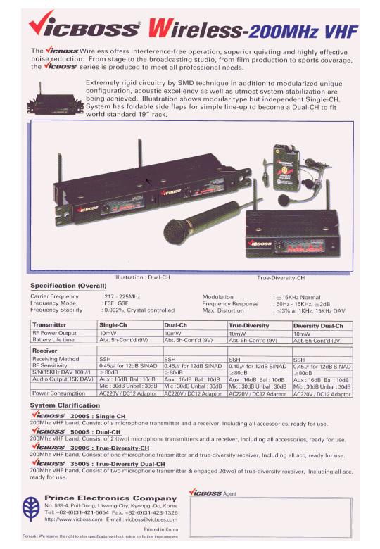
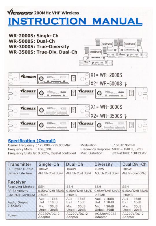
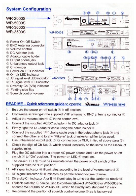
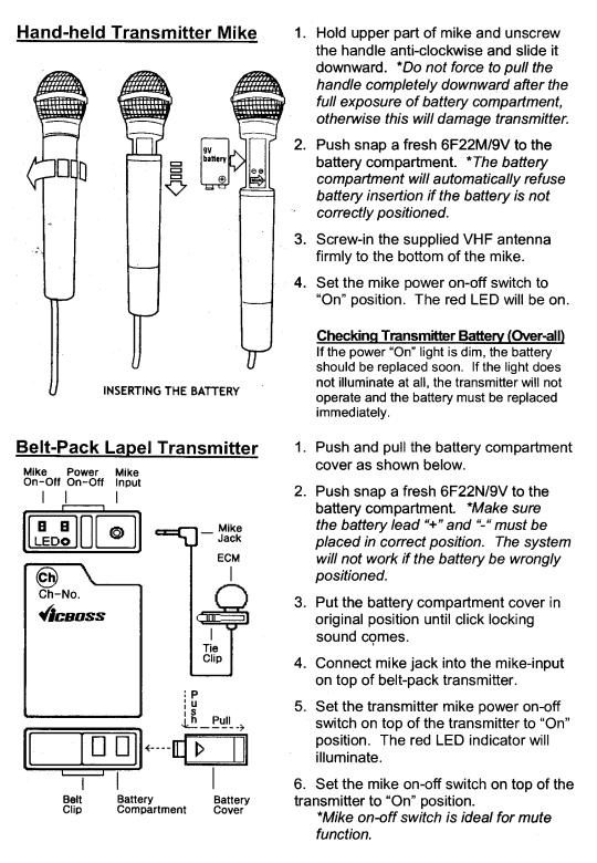
APPLICANT: PRINCE ELECTRONICS CO. FCC ID: NPXWM-205B TABLE OF CONTENTS LIST TEST REPORT CONTAINING: PAGE 1........ GENERAL INFORMATION PAGE 2.........DESCRIPTIONS PAGE 3.........R.F POWER OUTPUT PROCEDURE & MODULATION CHARACHTERISTICTS PAGE 4.........AUDIO FREQUENCY RESPONSE PAGE 5.........MODULATION LIMITING PLOT – 300Hz PAGE 6.........MODULATION LIMITING PLOT – 1000Hz PAGE 7.........MODULATION LIMITING PLOT – 15000Hz PAGE 8.........OCCUPIED BANDWIDTH PAGE 9.........OCCUPIED BANDWIDTH PLOT PAGE 10........OCCUPIED BANDWIDTH PLOT - CW PAGE 11........RADIATED EMISSIONS TEST DATA & TEST PROCEDURE PAGE 12........METHOD OF MEASURING SPURIOUS EMISSIONS PAGE 13........FREQUENCY STABILITY TEST DATA PAGE 14........EQUIPMENT LIST EXHIBITS CONTAINING: EXHIBIT 1.......FCC ID LABEL SAMPLE & ID LABEL LOCATION EXHIBIT 2.......BLOCK DIAGRAM EXHIBIT 3A-3B...SCHEMATICS EXHIBIT 4.......TUNING PROCEDURE EXHIBIT 5.......CIRCUIT DESCRIPTION EXHIBIT 6.......USER'S MANUAL EXHIBIT 7.......TEST SET UP PHOTOGRAPH EXHIBIT 8A......EXTERNAL PHOTO – FRONT VIEW EXHIBIT 8B......EXTERNAL PHOTO – REAR VIEW EXHIBIT 9A......INTERNAL PHOTO – COPPER VIEW EXHIBIT 9B......INTERNAL PHOTO – COMPONENT VIEW EXHIBIT 10......SPECIFICATION SHEET APPLICANT: PRINCE ELECTRONICS CO. FCCID: NPXWM-205B REPORT #: P\PRINCE\1256K1\1256K1RPT.doc TABLE OF CONTENTS LIST GENERAL INFORMATION REQUIRED FOR TYPE ACCEPTANCE 2.1033(c)(1) PRINCE ELECTRONICS CO. will manufacture the NPXWM-205B 2.1033(c)(2) in quantity, for use under FCC RULES PART 74.801, LOW POWER AUXILIARY STATIONS. PRINCE ELECTRONICS CO. 200-1, MAESAN-RI, MOHYON-MYON YONGIN-CITY, KYONGGI-DO 449-853 KOREA 2.1033 TECHNICAL DESCRIPTION (c)(3) Instruction book. The instruction manual is in- cluded as Exhibit 6A-6H. (c)(4) Type of Emission: 130K0F3E Bn = 2M + 2DK M = 20000 D = 45kHz(Peak Deviation) K = 1 Bn = 2(20k) + 2(45k)(1) = 130k ALLOWED AUTHORIZED BANDWIDTH = 200kHz. 74.861(e)(5) (c)(5) Frequency Range: Part 74: 174-216MHz TEST FREQ = 214.5MHz. (c)(6) Power Range and Controls:UNIT has no controls. (c)(7) Maximum Output Power Rating: 0.10mWatts into 50 ohms resistive load. (c)(8) DC Voltages and Current into Final Amplifier: FINAL AMPLIFIER ONLY 9.0V BATTERY Vce = 9.0 Volts Ice = 34 mA. (c)(9) Tune-up procedure. The tune-up procedure is given in page 4A-4B. (c)(10) Complete Circuit Diagrams: The circuit diagram is included as EXHIBIT # 3A-3C. The block diagram is included as EXHIBIT #2. APPLICANT: PRINCE ELECTRONICS CO. FCCID: NPXWM-205B REPORT #: P\PRINCE\1256K1\1256K1RPT.doc PAGE #: 1 2.1033(c)11) Photo or Drawing of Label and sketch of location: See EXHIBIT # 1. 2.1033(c)12) Photos of Equipment: See EXHIBIT #'S 8A-10B. (c)(13) Description of all circuitry and devices provided for determining and stabilizing frequency. Description of any circuits or devices employed for suppression of spurious radiation, for limit- ing modulation, and for limiting power. This circuitry is described on page 5. Limiting Modulation: The transmitter audio circuitry is contained in IC101, IC102 and IC103. Limiting Power: There is no provision for limiting power. (13) Digital modulation. This unit does not use digital modulation. 2.1033(c)(14) The data required by 2.1046 through 2.1057 is submitted below. 2.1046 RF power output. RF power measured is: OUTPUT POWER: 0.10mWATTS APPLICANT: PRINCE ELECTRONICS CO. FCCID: NPXWM-205B REPORT #: P\PRINCE\1256K1\1256K1RPT.doc PAGE #: 2 R.F. POWER OUTPUT TEST PROCEDURE Transmitter 50 ohm under test Watt Meter Audio Oscillator 2.1047(a)(b) Modulation characteristics: AUDIO FREQUENCY RESPONSE The audio frequency response was measured in accordance with TIA/EIA Specification 603. The audio frequency response curve is shown on the next page. AUDIO LOW PASS FILTER The audiolow pass filter is not required in this unit. APPLICANT: PRINCE ELECTRONICS CO. FCCID: NPXWM-205B REPORT #: P\PRINCE\1256K1\1256K1RPT.doc PAGE #: 3 Prince Electronics WM-205B -50 -49 -48 -47 -46 -45 -44 -43 -42 100100010000100000 Frequency dBmV audio response PRINCE ELECTRONICS CO. FCC ID : NPXWM-205B JOB : 1256K1 PAGE # : 4 Modulation Limiting Prince Electronics WM-205B 0 5000 10000 15000 20000 25000 -61-51-41-31 dBmV Deviation 300 Hz PRINCE ELECTRONICS CO. FCC ID : NPXWM-205B JOB : 1256K1 PAGE # : 5 Modulation Limiting Prince Electronics WM-205B 0 5000 10000 15000 20000 25000 -60.5-50.5-40.5-30.5 dBmV Deviation 1000 Hz PRINCE ELECTRONICS CO. FCC ID : NPXWM-205B JOB : 1256K1 PAGE # : 6 Modulation Limiting Prince Electronics WM-205B 0 5000 10000 15000 20000 25000 -56-46-36 dBmV Deviation 15000 Hz C PRINCE ELECTRONICS CO. FCC ID : NPXWM-205B JOB : 1256K1 PAGE # : 7 2.1049(c) Occupied Bandwidth: Data in the plots show that all sidebands between 50 & 100% for the authorized bandwidth are attenuated by at least 25dB. From 100 to 250% of the authorize3d band- width they are attenuated by at least 35dB and beyond 250% 43 log(Po) dB. The plot shows the transmitter modulated with 15000 Hz(the highest modulation frequen- cy), adjusted for 50% modulation plus 16 dB. The spectrum analyzer was set with the unmodulated carrier at the top of the screen. The test procedure diagram and occupied bandwidth plots follow. Wireless Microphone transmitter: Test procedure diagram OCCUPIED BANDWIDTH MEASUREMENT Transmitter Coupler 50 ohm under test Resistive Load Audio Spectrum Oscillator Analyzer REQUIREMENT: PART 74: 200kHz EMISSION BANDWIDTH. APPLICANT: PRINCE ELECTRONICS CO. FCCID: NPXWM-205B REPORT #: P\PRINCE\1256K1\1256K1RPT.doc PAGE #: 8 2.1051 Spurious emissions at antenna terminals(conducted): Not Applicable no antenna connector. 2.1053(a)(b) Field strength of spurious emissions: NAME OF TEST: RADIATED SPURIOUS EMISSIONS REQUIREMENTS: Emissions must be 43 +10log(Po) dB below the mean power output of the transmitter. 43 + 10 log(0.01) = 23.00dB TEST DATA: Emission Frequency MHz ATTN dBC Margin dB 214.50 00.00 00.00 429.00 44.88 21.88 1,072.50 47.70 24.70 1,501.50 44.85 21.85 1,716.00 44.18 21.18 METHOD OF MEASUREMENT: …
Text truncated - open the document above for the full version.
Contact Information
Applicant
S D Lee(Manager)
Test Firm
Timco Engineering, Inc.S Sanders
Technical Specifications
| # | Rule Parts | Frequency Range | Power Output | Emission | Tolerance |
|---|---|---|---|---|---|
| 1 | 74 | 174 MHz - 216 MHz | 10.00 mW | 130KF3E | 50.0000000000 ppm |
Other Applications from Prince Electronics Co

NPXM70H-P070H071H
Mar 28, 2006Wireless Microphone System
Equipment Class
TNF - Licensed Non-Broadcast Transmitter Held to Face
NPXM70B-P070B071B
Mar 27, 2006Wireless Microphone System
Equipment Class
TBT - Licensed Broadcast Transmitter Worn on Body
NPXWR-2000S
Jan 15, 2002Wireless Receiver
Equipment Class
CXX - Communications Rcvr for use w/ licensed Tx and CBsNPXWM201B
Feb 16, 1998TBF - Licensed Broadcast Transmitter Held to Face
Equipment Class
TBF - Licensed Broadcast Transmitter Held to FaceNPXWR101S
Jan 27, 1998CYY - Communications Receiver used w/Pt 15 Transmitter
Equipment Class
CYY - Communications Receiver used w/Pt 15 Transmitter