NTX900Frequency Hopping Transmitter
Midway Services Inc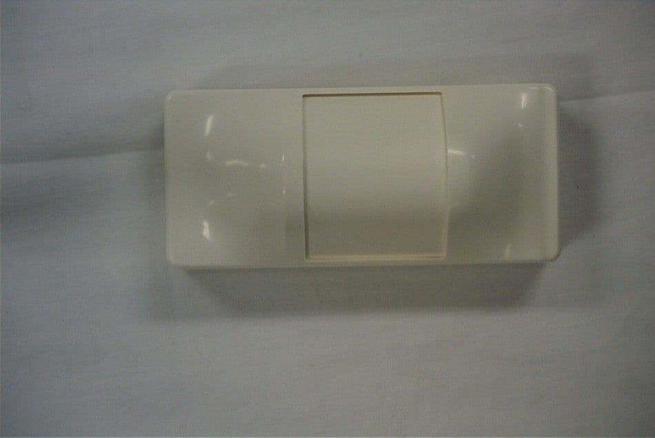
Click to zoom
Application Details
- Equipment Class
- DSS - Part 15 Spread Spectrum Transmitter
- Date of Grant
- Sep 06, 2001
- Application Purpose
- Original Equipment
- Date of Application
- Jun 10, 2001
- Equipment Note
- Frequency Hopping Transmitter
- Frequency Range
- 906.50000000 - 920.90000000
- Company
- Midway Services Inc
- Country
- United States
Documents & Files
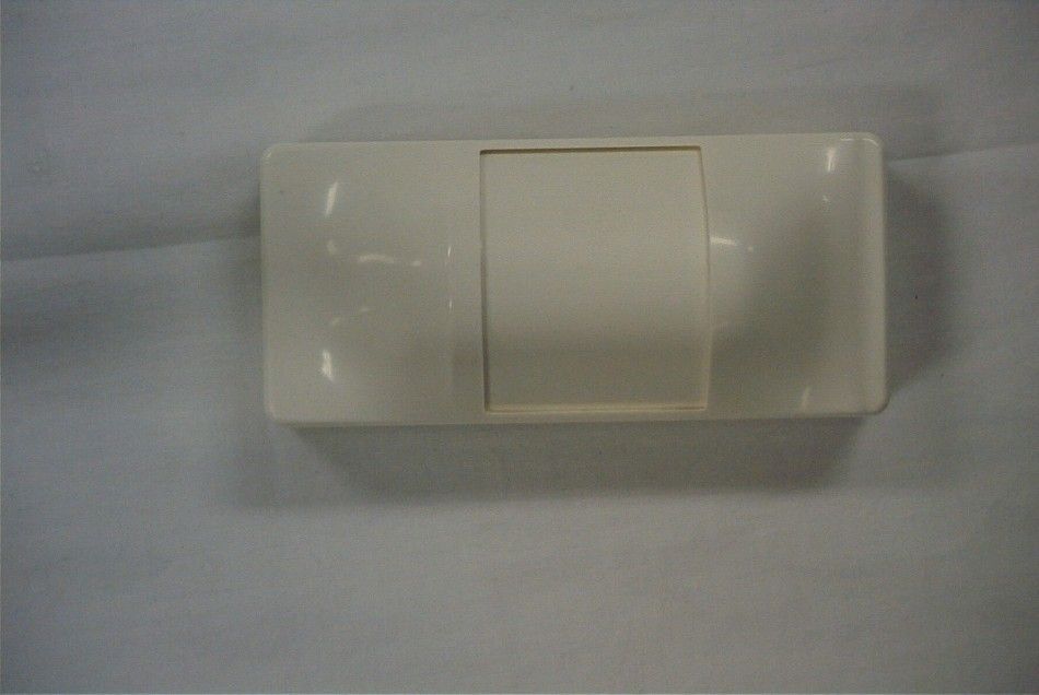
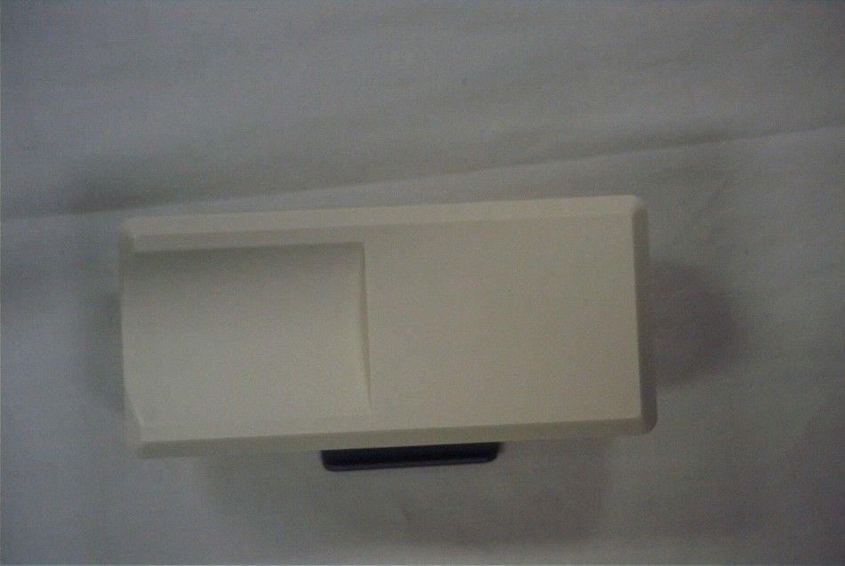
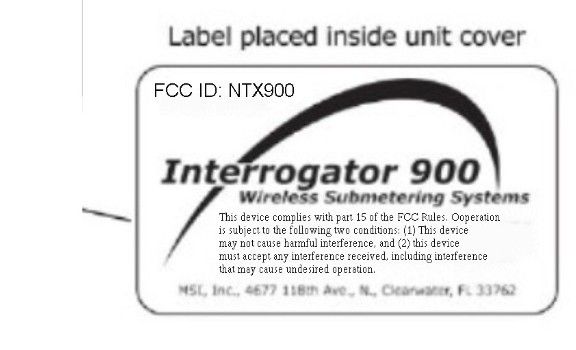
Document Text
Text extracted from the exhibit documents filed with the FCC. Open a document above to read the original.
Operational Description
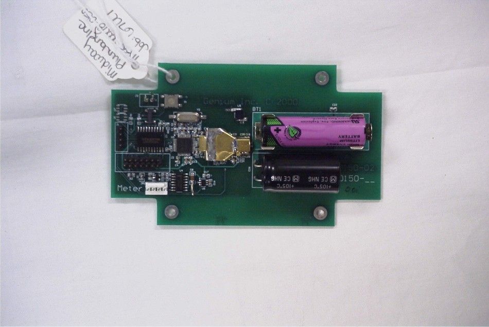
Genium Inc. 9720 131st Street N. Seminole, FL 33776 TEL: (727) 596-3052 FAX: (727) 596-9661 April 17, 2001 From:JF Stosic (Genium Inc.) and Judd Sheets (Odin Engineering) Subject:GW-900T Circuit Description for FCC Approval The GW900T transmitter circuit consists of three main functional areas: the user interface, the controller, and the RF section. User Interface. Meter data is read using a 3-wire interface on connector JP1. The clock required to interface the data is double-buffered by hex-inverter, U4. The switching regulator U5 provides the proper voltage to U4 and allows the processor to power-down the user interface during intervals when no data is schedule for transmission. Transistor Q1 is used on some interface configurations to buffer voltage pulses from "generated" type meters. Controller. The control processor, U2, reads the data from the user interface and formats the data for transmission. The control processor sends the transmit data packet to the RF section via the Tx_Data signal line. The frequency hopping algorithm is implemented in the control processor, which controls a direct digital synthesizer in the RF Section to select the current hop frequency. The processor also controls the power wake-up and power shutdown timing of the transmitter. Crystal Y1 is the processor clock and determines the transmit data rate. Switch S1 is used during installation to initiate a test sequence. Connector location J1 is used during manufacture to program the device. Connectors J2 and J3 were used during development but are unused in the manufactured device. Integrated Circuits U1 and U7 are unused in the manufactured device. RF Section. The RF section consists of a FSK exciter, a power amplifier, the battery, and an integrated antenna. The FSK exciter, U3, accepts frequency control data and transmit data from the controller to generate a modulated signal between 902 and 928 MHz. The exciter uses an integral direct digital synthesizer (DDS) to generate an internal intermediate frequency which is multiplied by an integral fixed ratio phase-lock loop (PLL) to generate the final frequency. Components C13, C15, R11, and R13 comprise the external loop filter for the PLL. C3, L1, C9 and D2 form the resonator of the PLL's voltage controlled oscillator. The modulation is digitally induced via a frequency deviation register in the DDS. Crystal Y2 provides the reference for the DDS. The power amplifier, U6, amplifies the 5 milliwatt, 900 MHz output of U3 to 250 milliwatts. The keying of the power amplifier is controlled directly from the control processor. The output filter section consists of inductors L4, L7, L14 and capacitors C19, C21, C28, C29. Geni um Inc. 2 The output of the output filter induces RF currents on the battery case to form the radiating element of the antenna. Inductor L6 blocks RF currents from entering the DC power that is supplied from the battery to the integrated circuits. Capacitor C26 is an energy storage device that maintains proper voltage levels during transmissions.
Operational Description
Genium Genium Inc.Inc.9720 131st Street N. Seminole, FL 33776 TEL: (727) 596-3052 FAX: (727) 596-9661 February 20, 2001 To:Mario de Aranzeta (Timco Engineering) From:JF Stosic (Genium Inc.) Subject:GW-900T FCC Data Modulation Parameters Modulation Type:Binary FSK Modulation Rate:10,932 bits per second Modulation Frequency Deviation:2f d = 16 kHz (peak-to-peak deviation) Pseudorandom Frequency Hopping Sequence Random Number Generator The frequency hop algorithm is generated from a maximal-length pseudo-random linear feedback shift register (LFSR). The LFSR is also known as the random number generator (RNG). In this design, the RNG shift register is 6 bits in length and generates a pseudo-random number from 1 to 63. The RNG used in the GW-900T is shown in Figure 1. The RNG taps were selected based on a well-known LFSR design with good statistical properties that is free of long sequential runs. Each new value of the RNG is generated by the following steps: 1. Logically add b 5 to b 4 and save the result in a delay register, D. 2. Shift the bits in the shift register to the left such that b 4 > b 5 , b 3 > b 4 , ... 3. Shift the delay register, D, into b 0 . DRAFT Genium Inc. 2 b 0 b 1 b 2 b 3 b 4 b 5 +D Figure 1. Random Number Generator. An example of the random number generator output is shown in Table 1. Here the initial value of R, that is R 1 , was set to 31. The second value of R, that is R 2 , is computed to be 63. The third computed value of R, R 3 , is 62. The 64 th time the RNG is updated, the value of R is computed to be 31 and the sequence starts over. Table 1. Random Number Generator Output. Number of Times R is Computed Value of R R 1 31 R 2 63 R 3 62 ...... R 62 23 R 63 47 R 64 = R 1 31 R 65 = R 2 63 Hop Frequencies Each hop period, a new value R, from 1 to 63, is computed from the RNG. The hop frequency for the current hop is computed by the following equation: f h = 905.700 + 0.100 * (N-1) + 0.300R [MHz] Here, N is a net number from 1 to 3 which is set at the time of manufacture and gives additional frequency diversity to radios nets that are deployed. Table 2 shows examples of the hop frequency calculation. DRAFT Genium Inc. 3 Table 2. Hop Frequency, f h , in MHz. Net Number, N Value of R123 R = 1906.000906.100906.200 R = 2906.300906.400906.500 ............ R = 63924.600924.700924.800 Equal Hopping Frequency Use Each message sent from a transmitter is divided into 10 separate parts. Each of the 10 parts is sent on a separate frequency (hop). The duration of a single hop is greater than 4.5 msec and less than 20 msec. There is a 10 second delay between each hop. At the beginning of each hop, a new value, R, from random number generator is computed in accordance with Figure 1. When a new message is to be sent, the process is continued where the next value of R is computed in accordance with Figure 1. The initial value of R is set only once and occurs only when the radio is installed or when the battery requires replacement. Table 3 shows an example of how the hop pattern is distributed among sequential messages. Here R 1 is the first random number computed from the RNG, R 2 is the second number computer from the RNG, etc. Note that the value of R 1 is not 1 and the value of R 2 is not 2. The values of R are determined as shown in Table 1. Table 3. Distributions of Hops Across Multiple messages. Msg Part 1 Msg Part 2 Msg Part 3 Msg Part 4 Msg Part 5 Msg Part 6 Msg Part 7 Msg Part 8 Msg Part 9 Msg Part 10 Message 1R 1 R 2 R 3 R 4 R 5 R 6 R 7 R 8 R 9 R 10 Message 2R 11 R 12 R 13 R 14 R 15 R 16 R 17 R 18 R 19 R 20 • • • Message 6R 51 R 52 R 53 R 54 R 55 R 56 R 57 R 58 R 59 R 60 Message 7R 61 R 62 R 63 R 1 R 2 R 3 R 4 R 5 R 6 R 7 DRAFT Genium Inc. 4 System Receiver Input Bandwidth The associated receiver uses a digital signal processor to implement a 3 rd order CIC i filter to match the receiver bandwidth to the transmitted signal. System Receiver Hopping Capability The associated receiver uses a digital quadrature tuner to shift frequencies in synchronization with the transmitted signal. A 32-bit unique-word synchronization sequence is used to detect initial synchronization. i CIC – Cascade-Integrator-Comb filter. This is an efficient class of finite impulse response (FIR) digital filters that operate without the use of digital multipliers. This is a common technique used in modern communication systems such as digitally implemented cell phone receivers. Reference: Hogenauer, Eugene, “An Economical Class of Digital Filters for Decimation and Interpolation”, IEEE Transactions on Acoustics, Speech and Signal Processing, Vol. ASSP-29 No. 2, April 1981.
RF Exposure Info
IMPORTANT NOTICE AND SAFETY INFORMATION This device contains a low power transmitter. When the device is in use it sends out radio frequency (RF) signals. In August 1996, the Federal Communications Commission (FCC) adopted RF exposure guidelines with safety levels for wireless devices. Use only the supplied antenna. Unauthorized antennas,modifications, or attachments could damage the transmitter and may violate FCC regulations.
RF Exposure Info
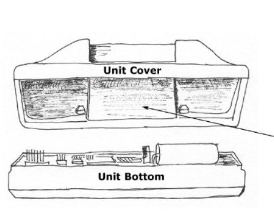
Timco Engineering 849 NW SR45 Newberry FL 32669 MPE evaluation for Midway Plumbing Model NTX900. Description of device and typical operating conditions. The RF transmitter is a frequency hopping 900 MHz device. This device is used to instrument an utility meter for remote reading. It has an RF conducted output power of 252 mW and an antenna gain of -2.67 dB. This device has a plastic cover over it that keeps the antenna a minimum distance of 1 cm away from everything. The operation cycle of this device worst case is 15 msec. ON followed by 2 seconds OFF repeated 15 times on initial startup and then one 15 msec.ON transmission every 30 minutes. This makes for a worst case ON time in 30 minutes of 240 msec.. MPE calculation based on a 20 cm separation are shown below for a 100% ON time. GdB2.67 gain of ant in dB G10 GdB 10 G0.541 = gain of antenna P252R120 P is power in mW R1 is distance in cm MPG . S1 PG . 4 π R1 2 . M136.27 = S10.027 = Power density in mW/cm^2 From Table 1 in OET 65 (page67) the general population/uncontrolled exposure limits for a 915 MHz device is 915/1500 or 0.61 mW/cm^2.
Test Report
APPLICANT: MIDWAY SERVICES, INC. FCC ID: NTX900 TABLE OF CONTENTS TEST REPORT CONTAINING: PAGE 1.............TEST PROCEDURE PAGE 2.............TEST PROCEDURE PAGE 3.............EQUIPMENT LIST PAGE 4.............GENERAL INFORMATION PAGE 5.............POWER OUTPUT PAGE 6.............RF CONDUCTED EMISSIONS PAGE 7.............RADIATION INTERFERENCE TEST DATA PAGE 8.............METHOD OF MEASURING RADIATED SPURIOUS EMISSIONS EXHIBIT ATTACHMENTS: EXHIBIT 1...........FCC ID LABEL SAMPLE EXHIBIT 2...........SKETCH OF FCC ID LABEL LOCATION EXHIBIT 3...........TEST SETUP PHOTOGRAPH EXHIBIT 4...........EXTERNAL PHOTOGRAPH – FRONT VIEW EXHIBIT 5...........EXTERNAL PHOTOGRAPH – REAR VIEW EXHIBIT 6...........INTERNAL PHOTOGRAPH – COMPONENT VIEW EXHIBIT 7...........INTERNAL PHOTOGRAPH – SOLDER VIEW EXHIBIT 8...........BLOCK DIAGRAM EXHIBIT 9...........CHANNEL SPACING EXHIBIT 10..........20 dB BANDWIDTH OF A HOPPPING CHANNEL EXHIBIT 11..........DEWLL TIME PLOT EXHIBIT 12..........BANDEDGE PLOTS – 20 dB EXHIBIT 13A-13D.....NO. OF CHANNELS PLOTS EXHIBIT 14..........CIRCUIT DESCRIPTION EXHIBIT 15..........HOPPING INFORMATION EXHIBIT 16..........SCHEMATICS EXHIBIT 17..........USERS MANUAL APPLICANT: MIDWAY SERVICES, INC. FCC ID: NTX900 REPORT NO.: M/MIDWAY\67u1\67u1TestReport.doc PAGE #: TABLE OF CONTENTS TEST PROCEDURE GENERAL: This report shall NOT be reproduced except in full without the written approval of TIMCO ENGINEERING, INC. The UUT was transmit- ting a test signal during the testing. 15.247(a)(1) CARRIER FREQUENCY SEPARATION & NUMBER OF CHANNELS: A near field probe was used to sense the signal of the UUT. The UUT was made to hop its full range. The spectrum analyzer was set to view the frequency range from 902 to 928 MHz and placed in the memory mode. A plot (Exhibit #9) was then made of the display showing the number of channels, 63 and the separation of the channels, 115 kHz. 15.247(a)(1)(i) CARRIER FREQUENCY DWELL TIME: A near field probe was used to sense the signal of the UUT. The UUT was made to hop its full range. The spectrum analyzer was set to view the frequency range from 902 to 928 MHz and the center of the HOPPING RANGE was centered on the Spectrum Analyzer. The SPAN was then set to ZERO(0) and the SWEEP TIME was set to 20 seconds. Then by analyzing the plot of the total ON TIME of the UUT during the 20 seconds it was determined the dwell time on any frequency was less than 0.4 seconds, 14.4 mseconds. See exhibit #11. 15.247(b)(2) POWER OUTPUT: The RF power output was measured at the antenna feed point by removing the permanent antenna and connecting the UUT to a peak power meter, HP Model No. 8900C. 15.247(c) ANTENNA CONDUCTED EMISSIONS: The RBW=100 kHz, VBW =1.0 MHz up to 1000 MHz and RBW=1.0MHz & VBW=3.0 MHz above 1.0 GHz. The spectrum was scanned from 30 MHz to the 10th Harmonic of the fundamental. RADIATION INTERFERENCE: The test procedure used was ANSI STANDARD C63.4-1992 using a HEWLETT PACKARD spectrum analyzer with a prese- lector. The analyzer was calibrated in dB above a microvolt at the output of the antenna. The resolution bandwidth was 100 kHz and the video bandwidth was 300 kHz up to 1.0 GHz and 1.0 MHz with a video BW of 3.0 MHz above 1.0 GHz. The ambient temperature of the UUT was 87°F, with a humidity of 29%. The hopping was stopped at the low end, middle and high end of the band in order to test the radiated emis- sions. POWER LINE CONDUCTED INTERFERENCE: The procedure used was ANSI STANDARD C63.4-1992 using a 50uH LISN. Both lines were observed. The bandwidth of the spectrum analyzer was 10 kHz with an appro- priate sweep speed. The ambient temperature of the UUT was 78°F with a humidity of 45%. APPLICANT: MIDWAY SERVICES, INC. FCC ID: NTX900 REPORT #: M/MIDWAY\67u1\67u1TestReport.doc PAGE #: 1 TEST PROCEDURES CONTINUED FORMULA OF CONVERSION FACTORS: The Field Strength at 3 m was estab- lished by adding the meter reading of the spectrum analyzer (which is set to read in units of dBuV) to the antenna correction factor supplied by the antenna manufacturer. The antenna correction factors are stated in terms of dB. The gain of the Preselector was accounted for in the Spectrum Analyzer Meter Reading. Example: Freq (MHz) METER READING + ACF = FS 33 20 dBuV + 10.36 dB = 30.36 dBuV/m @ 3m APPLICANT: MIDWAY SERVICES, INC. FCC ID: NTX900 REPORT #: M/MIDWAY\67u1\67u1TestReport.doc PAGE #: 2 TEST EQUIPMENT LIST 1._X_Spectrum Analyzer: HP 8566B-Opt 462, S/N 3138A07786, w/ preselector HP 85685A, S/N 3221A01400, Quasi-Peak Adapter HP 8565OA, S/N 3303A01690 & Preamplifier HP 8449B-OPT H02, S/N 3008A00372 2._X_Biconnical Antenna: Eaton Model 94455-1, S/N 1057, 3.___Biconnical Antenna: Electro-Metrics Model BIA-25, S/N 1171 4._X_Log-Periodic Antenna: Electro-Metrics Model EM-6950, S/N 632 5.___Log-Periodic Antenna: Electro-Metrics Model LPA-30, S/N 409 6._X_Double-Ridged Horn Antenna: Electro-Metrics Model RGA-180, 1-18 GHz, S/N 2319 7.___18-26.3GHz Systron Donner Standard Gain Horn #DBE-520-20 8.___Horn 40-60GHz: ATM Part #19-443-6R 9.___Line Impedance Stabilization Network: Electro-Metrics Model EM-7820, w/NEMA Adapter S/N 2682 10.___Temperature Chamber: Tenney Engineering Model TTRC, S/N 11717-7 11.___Frequency Counter: HP Model 5385A, S/N 3242A07460 12.___Peak Power Meter: HP Model 8900C, S/N 2131A00545, 13._X_Open Area Test Site #1-3 meters 14.___Signal Generator: HP 8640B, S/N 2308A21464 15.___Signal Generator: HP 8614A, S/N 2015A07428 16.___Passive Loop Antenna: EMCO Model 6512, 9KHz to 30MHz, S/N 9706-1211 17.___Dipole Antenna Kit: Electro-Metrics Model TDA-30/1-4, S/N 153 18.___AC Voltmeter: HP Model 400FL, S/N 2213A14499 19.___Digital Multimeter: Fluke Model 8012A, S/N 4810047 20.___Digital Multimeter: Fluke Model 77, S/N 43850817 21.___Oscilloscope: Tektronix Model 2230, S/N 300572 APPLICANT: MIDWAY SERVICES, INC. FCC ID: NTX900 REPORT #: M/MIDWAY\67u1\67u1TestReport.doc PAGE #: 3 INTRODUCTION: GENERAL INFORMATION AND DATA 15.247(a): Definition: This EUT uses a pseudo ran…
Text truncated - open the document above for the full version.
Contact Information
Applicant
Steven C. Tilka
Technical Contact
Timco Engineering, Inc.Mario R de Aranzeta
[email protected]888-472-2424
849 N.W. State Road 45 · Newberry, Florida · United States
Non-Technical Contact
Timco Engineering, Inc.Sharon A Hoffman
[email protected]888-472-2424
Test Firm
Timco Engineering, Inc.S Sanders
Technical Specifications
| # | Rule Parts | Frequency Range | Power Output |
|---|---|---|---|
| 1 | 15C | 906.5 MHz - 920.9 MHz | 252.00 mW |
Other Applications from Midway Services Inc
NTXINT900
Jul 24, 2003902-928 SPREAD SPECTRUM TRANSCEIVER UNIT
Equipment Class
DSS - Part 15 Spread Spectrum Transmitter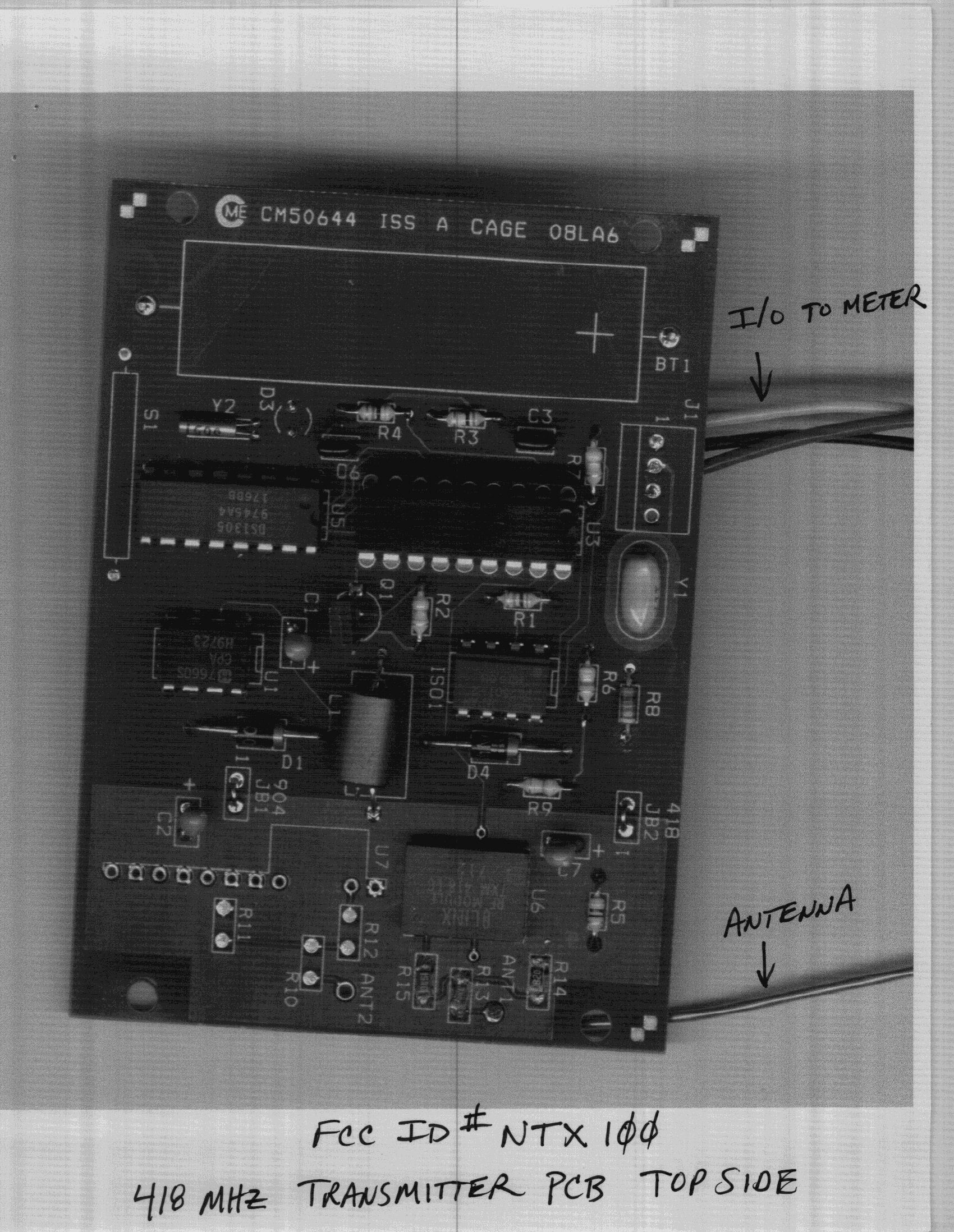
NTX100
Jun 28, 1998Water Meter Transmitter
Equipment Class
DSC - Part 15 Security/Remote Control Transmitter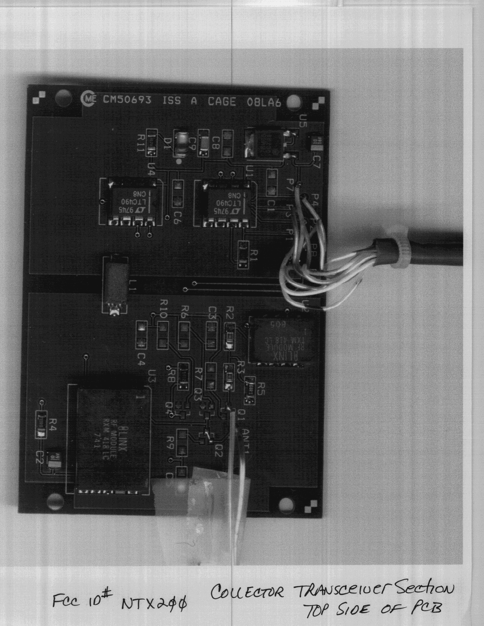
NTX200
Jun 18, 1998Meter data collector
Equipment Class
DXT - Part 15 Low Power Transceiver, Rx Verified