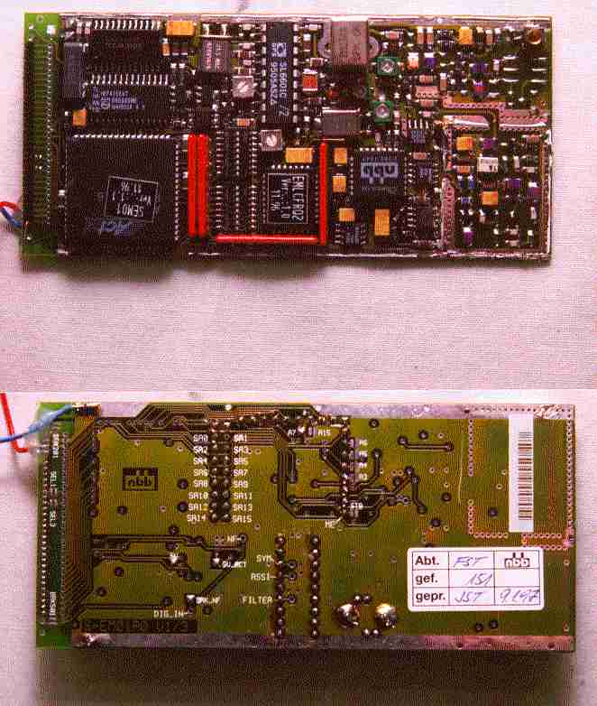
O5RS-DE96AOCrane Remote Control
NBB Nachrichtentechnik GmbH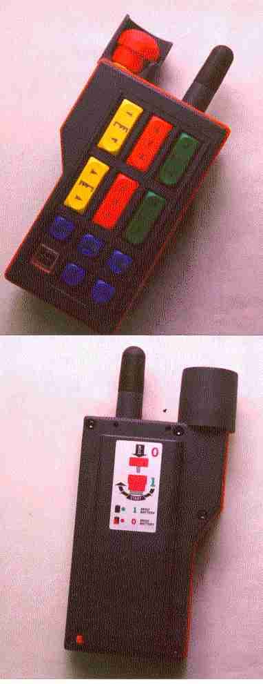
Click to zoom
Application Details
- Equipment Class
- DSC - Part 15 Security/Remote Control Transmitter
- Date of Grant
- Apr 12, 2001
- Application Purpose
- Original Equipment
- Date of Application
- Mar 26, 2001
- Equipment Note
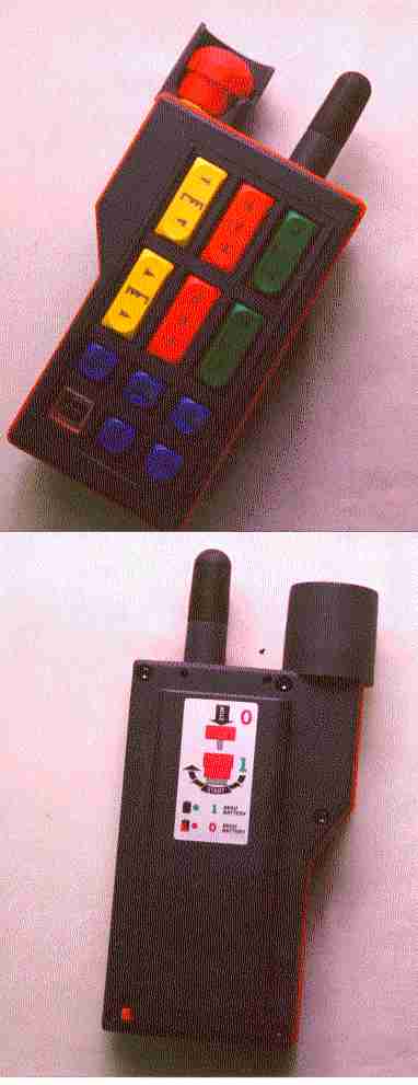
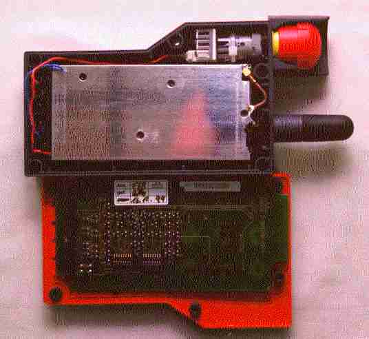
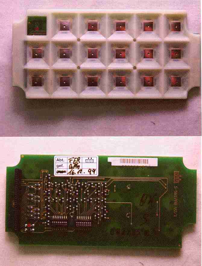
- Crane Remote Control
- Frequency Range
- 903.00000000 - 922.00000000
- Company
- NBB Nachrichtentechnik GmbH
- Country
- Germany
Documents & Files
Document Text
Text extracted from the exhibit documents filed with the FCC. Open a document above to read the original.
Block Diagram
NBB Nachrichtentechnik GmbH & Co. KG Sender 900MHz.doc Page 1 / 20 20.01.2000 Contents S-DE96A0 - Transmission module 1.Specification of the module S-DE96A0 2 1.1Description of transmission module S-DE96A0 3 1.2RF technology of the module S-DE96A0 4 1.3Circuit diagrams, component plot, layout, bill of material for module S-DE96A0 5 NBB Nachrichtentechnik GmbH & Co. KG Sender 900MHz.doc Page 2 / 20 20.01.2000 1. Specification of transmission module S-DE96A0 Frequency:902MHz - 928MHz Power supply:5.4V DC to 9 V DC Licence: Application:Radio equipment for commercial and industrial remote control and telemetering Radiated transmitter power:<10mW; 50 Ohm HF modulation:FM Type of transmission:F 1 D Channel spacing:25 kHz NBB Nachrichtentechnik GmbH & Co. KG Sender 900MHz.doc Page 3 / 20 20.01.2000 1.1 The transmission module S-DE96A0 The module S-DE96A0 is a single PCB solution, on which the RF transmitter, AF section and data processing are integrated. A data interface exists that reads in binary data via an 8-bit-wide bus. This binary data is processed in an FPGA (Field Programmable Gate Array) and passed via a D/A converter as an FSK signal to CCITT V.23 to the RF unit. After switch-on of the transmitter the FPGA reads in the frequency programmed once by NBB and thereby permits initialisation of the synthesizer. Once the latter has been initialised, data transmission commences. Fig. 1.1.1: Block diagram S-DE96A0 Signal pro- cessing unit (noise-free - coding of data) D0 . . . D7 SEL 0 . . . SEL 10 Electronic con- egel- und Steuer- trol unit D A RF part Transmitter antenna Modulation of serially arriving data 7.2V ∆ U U=const S-DE96A0 NBB Nachrichtentechnik GmbH & Co. KG Sender 900MHz.doc Page 4 / 20 20.01.2000 1.2 RF circuitry of module S-DE96A0 When the transmitter is switched on, or when there is a positive or negative pulse at the reset input of the PLL module from the FPGA ACT42MX09 or ACT42MX16, it automatically reads out 8 times 4 bits from the EEPROM 28C256. The EEPROM only remains energized until all the data has been read out (to save power). The data corresponds to a frequency and is used by the PLL module as information for programming its own scaler. Since the scaler of the PLL IC's only functions up to a maximum of 10 MHz, an RF prescaler (U3) is needed which has a division ratio of 64/128 up to approx. 1000 MHz. The RF power for the prescaler is tapped from the output of LO1 over a coupling conductor. The RF that has now been scaled down to the reference frequency of 20 kHz (= channel increment) is compared with the signal that has also been scaled down from the reference frequency of 12.8 MHz and any deviation (coarse and fine) is fed to an integrator which produces the control supply for the variable capacitance diode in the voltage-controlled RF oscillator. The RF oscillator is of the harmonic type and is isolated from the now 2-stage amplifier by an extra filter. This is necessary in order to minimize the feedback between aerial and oscillator and to suppress the remaining harmonics. And, of course, no pre-stage, mixer, SAW, LO2 or demodulator module are needed in the transmitter. The modulation, on the other hand, is produced at the duplex variable capacitance diode in the oscillator. NBB Nachrichtentechnik GmbH & Co. KG Sender 900MHz.doc Page 5 / 20 20.01.2000 1.3 Circuit diagrams, component plot, layout, bill of material for module S-DE96A0 NBB Nachrichtentechnik GmbH & Co. KG Sender 900MHz.doc Page 6 / 20 20.01.2000 1 2 1 2 1 2 1 2 1 2 1 2 1 2 1 2 12 12 12 12 1 2 1 2 1 2 1 2 1 2 1 2 3 4 56789 10111213 14 15 16 17 18 19 20 212223242526272829 30 31 32 1 2 1 2 1 2 1 2 1 2 1 2 1 2 17 12 1 2 12 1 2 12 1 2 12 1614131211109876153213231302928 7 65 84 12 12 1234 5678 1 2 12 12 12 12 23 1 12 272625242322 3 2 212019 79 45 70 46 68 78 62 61 4 77 76 75 32 31 30 40 90 29 28 27 26 72 25 24 23 21 20 19 18 15 7374822212139947511752537154559663338180 42 43 50 44 49 48 9 86 87 83 85 35 36 34 66 65 67 37 38 95 94 57 89 98 92 88 93 41 97 39 56911184 100 1459 1 6016 2 58 3 69 5 64 678 10 1 2 1854 1 2 1 2 1 2 1 2 1 2 1 2 1 2 1 2 1 2 1 2 1 2 1 2 1 2 1 2 1 2 1 2 1 2 1 2 1 2 1 2 1 2 1 2 1 2 1 2 1 2 1 2 1 2 1 2 1 2 1 2 1 2 1 2 1 2 1 2 1 2 1 2 1 23 4 1 2 1 2 12 1 2 R104R105R106R107R101 R109 R108R102 C102 C101 R111 R110 X101 C112 C114 C111 C118 U102 BRK101BRK104BRK105BRK106BRK107BRK108BRK102 ST1 C108 R119 C109 R118 C106 R117 R116 ST1ST1ST1ST1ST1ST1ST1ST1ST1ST1ST1ST1ST1ST1ST1ST1ST1ST1ST1 +- U403 C103 C104 U103 R129 R115 R113 R112 C105 Q101 R114 ST1ST1ST1ST1ST1ST1 D101 ST1ST1ST1 U101 C110 ST1ST1ST1 BRK109 R121R122R123R124R125R126R127R128R120 C120C122C124C126C128C130C132C134C136C138C140 C113 C115 C117C119C121 C123 C125 C127C129 C131C133 C135C137C139 C141 12.8MHz G N1 BRK110 R130 R131 C116 AGND AGND AGND AGND AGNDAGND AGND AGND AGND AGND AGND AGND AGND AGND AGND AGND AGND AGND AGND AGND AGND AGND AGND AGND PDB A6 A6 A7 A7 A8 A8 A9 A9 AMP PDA PB_1 PB_1 SEL13 SEL13 SEL13 D5 D5 D5 D5 D7 D7 D7 D7 TEILER A2 A2 A2 A2 Q3 Q2 Q1 Q0 T0 CE CE CECECE 12.8MHZ 12.8MHZ 12.8MHZ A0 A0 A0 A0 SEL0 SEL0 SEL0 LED1 LED1 ONRES VDAT WE WE D6 D6 D6 D6 D4 D4 D4 D4 D3 D3 D3 D3 D2 D2 D2 D2 D1 D1 D1 D1 D0 D0 D0 D0 Q4 SEL14 SEL14 SEL14 OE OE OEOE SEL3 SEL3 SEL3 SEL6 SEL6 SEL6 SEL7 SEL7 SEL7 SEL8 SEL8 SEL8 SEL9 SEL9 SEL9 SEL10 SEL10 SEL10 SEL11 SEL11 SEL11 SEL12 SEL12 SEL12 SEL2 SEL2 SEL2 ACCU ACCU LED2 LED2 Q5 A4 A4 A5 A5 SEL4 SEL4 SEL4 SEL5 SEL5 SEL5 SEL1 SEL1 SEL1 A3 A3 A3 A3 USK PA_1 PA_1 MCI MCI CONF CONF E14 E14 SW +5VB +5VB +5VB +5VB +5VB +5VB +5VB +5VB +5VB +5VB +5VB +5VB +5VB MC NC A1 A1 A1 A1 A10 A10 A10A10A10 A11 A11 A12 A12 A13 A13 A14 A14 E10 E10 E11 E11 E12 E12 E13 E13 BRK110 BRK110 28Cxx MAX907 93C46 BAT54 ACT2 Family TCXO 2.100.1099.25 S-DE96A0 V2/5 S-DE9601.SCH FILE 07.05.98 of 5 18.10.97 APPROVED UmhauUmhau c 75248 OELBRONN-DUERRN ENCODER OTTO-HAHN-STR.3 TECHNIKNACHRICHTENNBB 2 88 77 66 55 44 33 2 11 D D C C B B A A SCALE DWG. NO. FSCM NO. SIZE REV. SHEET DATE APPROVALS D CONTRACT NO.DRAWNCHECKED NC/A11 NC/A12 NC/A…
Text truncated - open the document above for the full version.
ID Label/Location Info
FCCID LABEL FORMAT AND LOCATION POCKET-S SERIAL NO. 989XXXXXXXXXXX FCCID: O5RS-DE96A0 This device complies with Part 15 of the FCC Rules. Operation of this device is subject to the following conditions: (1) This device may not cause harmful interference, and (2) this device must accept any interference received, including interference which may cause undesired operation. MADE IN GERMANY
Operational Description
NBB Nachrichtentechnik GmbH & Co. KG Sender 900MHz.doc Page 1 / 20 20.01.2000 Contents S-DE96A0 - Transmission module 1.Specification of the module S-DE96A0 2 1.1Description of transmission module S-DE96A0 3 1.2RF technology of the module S-DE96A0 4 1.3Circuit diagrams, component plot, layout, bill of material for module S-DE96A0 5 NBB Nachrichtentechnik GmbH & Co. KG Sender 900MHz.doc Page 2 / 20 20.01.2000 1. Specification of transmission module S-DE96A0 Frequency:902MHz - 928MHz Power supply:5.4V DC to 9 V DC Licence: Application:Radio equipment for commercial and industrial remote control and telemetering Radiated transmitter power:<10mW; 50 Ohm HF modulation:FM Type of transmission:F 1 D Channel spacing:25 kHz NBB Nachrichtentechnik GmbH & Co. KG Sender 900MHz.doc Page 3 / 20 20.01.2000 1.1 The transmission module S-DE96A0 The module S-DE96A0 is a single PCB solution, on which the RF transmitter, AF section and data processing are integrated. A data interface exists that reads in binary data via an 8-bit-wide bus. This binary data is processed in an FPGA (Field Programmable Gate Array) and passed via a D/A converter as an FSK signal to CCITT V.23 to the RF unit. After switch-on of the transmitter the FPGA reads in the frequency programmed once by NBB and thereby permits initialisation of the synthesizer. Once the latter has been initialised, data transmission commences. Fig. 1.1.1: Block diagram S-DE96A0 Signal pro- cessing unit (noise-free - coding of data) D0 . . . D7 SEL 0 . . . SEL 10 Electronic con- egel- und Steuer- trol unit D A RF part Transmitter antenna Modulation of serially arriving data 7.2V ∆ U U=const S-DE96A0 NBB Nachrichtentechnik GmbH & Co. KG Sender 900MHz.doc Page 4 / 20 20.01.2000 1.2 RF circuitry of module S-DE96A0 When the transmitter is switched on, or when there is a positive or negative pulse at the reset input of the PLL module from the FPGA ACT42MX09 or ACT42MX16, it automatically reads out 8 times 4 bits from the EEPROM 28C256. The EEPROM only remains energized until all the data has been read out (to save power). The data corresponds to a frequency and is used by the PLL module as information for programming its own scaler. Since the scaler of the PLL IC's only functions up to a maximum of 10 MHz, an RF prescaler (U3) is needed which has a division ratio of 64/128 up to approx. 1000 MHz. The RF power for the prescaler is tapped from the output of LO1 over a coupling conductor. The RF that has now been scaled down to the reference frequency of 20 kHz (= channel increment) is compared with the signal that has also been scaled down from the reference frequency of 12.8 MHz and any deviation (coarse and fine) is fed to an integrator which produces the control supply for the variable capacitance diode in the voltage-controlled RF oscillator. The RF oscillator is of the harmonic type and is isolated from the now 2-stage amplifier by an extra filter. This is necessary in order to minimize the feedback between aerial and oscillator and to suppress the remaining harmonics. And, of course, no pre-stage, mixer, SAW, LO2 or demodulator module are needed in the transmitter. The modulation, on the other hand, is produced at the duplex variable capacitance diode in the oscillator. NBB Nachrichtentechnik GmbH & Co. KG Sender 900MHz.doc Page 5 / 20 20.01.2000 1.3 Circuit diagrams, component plot, layout, bill of material for module S-DE96A0 NBB Nachrichtentechnik GmbH & Co. KG Sender 900MHz.doc Page 6 / 20 20.01.2000 1 2 1 2 1 2 1 2 1 2 1 2 1 2 1 2 12 12 12 12 1 2 1 2 1 2 1 2 1 2 1 2 3 4 56789 10111213 14 15 16 17 18 19 20 212223242526272829 30 31 32 1 2 1 2 1 2 1 2 1 2 1 2 1 2 17 12 1 2 12 1 2 12 1 2 12 1614131211109876153213231302928 7 65 84 12 12 1234 5678 1 2 12 12 12 12 23 1 12 272625242322 3 2 212019 79 45 70 46 68 78 62 61 4 77 76 75 32 31 30 40 90 29 28 27 26 72 25 24 23 21 20 19 18 15 7374822212139947511752537154559663338180 42 43 50 44 49 48 9 86 87 83 85 35 36 34 66 65 67 37 38 95 94 57 89 98 92 88 93 41 97 39 56911184 100 1459 1 6016 2 58 3 69 5 64 678 10 1 2 1854 1 2 1 2 1 2 1 2 1 2 1 2 1 2 1 2 1 2 1 2 1 2 1 2 1 2 1 2 1 2 1 2 1 2 1 2 1 2 1 2 1 2 1 2 1 2 1 2 1 2 1 2 1 2 1 2 1 2 1 2 1 2 1 2 1 2 1 2 1 2 1 2 1 23 4 1 2 1 2 12 1 2 R104R105R106R107R101 R109 R108R102 C102 C101 R111 R110 X101 C112 C114 C111 C118 U102 BRK101BRK104BRK105BRK106BRK107BRK108BRK102 ST1 C108 R119 C109 R118 C106 R117 R116 ST1ST1ST1ST1ST1ST1ST1ST1ST1ST1ST1ST1ST1ST1ST1ST1ST1ST1ST1 +- U403 C103 C104 U103 R129 R115 R113 R112 C105 Q101 R114 ST1ST1ST1ST1ST1ST1 D101 ST1ST1ST1 U101 C110 ST1ST1ST1 BRK109 R121R122R123R124R125R126R127R128R120 C120C122C124C126C128C130C132C134C136C138C140 C113 C115 C117C119C121 C123 C125 C127C129 C131C133 C135C137C139 C141 12.8MHz G N1 BRK110 R130 R131 C116 AGND AGND AGND AGND AGNDAGND AGND AGND AGND AGND AGND AGND AGND AGND AGND AGND AGND AGND AGND AGND AGND AGND AGND AGND PDB A6 A6 A7 A7 A8 A8 A9 A9 AMP PDA PB_1 PB_1 SEL13 SEL13 SEL13 D5 D5 D5 D5 D7 D7 D7 D7 TEILER A2 A2 A2 A2 Q3 Q2 Q1 Q0 T0 CE CE CECECE 12.8MHZ 12.8MHZ 12.8MHZ A0 A0 A0 A0 SEL0 SEL0 SEL0 LED1 LED1 ONRES VDAT WE WE D6 D6 D6 D6 D4 D4 D4 D4 D3 D3 D3 D3 D2 D2 D2 D2 D1 D1 D1 D1 D0 D0 D0 D0 Q4 SEL14 SEL14 SEL14 OE OE OEOE SEL3 SEL3 SEL3 SEL6 SEL6 SEL6 SEL7 SEL7 SEL7 SEL8 SEL8 SEL8 SEL9 SEL9 SEL9 SEL10 SEL10 SEL10 SEL11 SEL11 SEL11 SEL12 SEL12 SEL12 SEL2 SEL2 SEL2 ACCU ACCU LED2 LED2 Q5 A4 A4 A5 A5 SEL4 SEL4 SEL4 SEL5 SEL5 SEL5 SEL1 SEL1 SEL1 A3 A3 A3 A3 USK PA_1 PA_1 MCI MCI CONF CONF E14 E14 SW +5VB +5VB +5VB +5VB +5VB +5VB +5VB +5VB +5VB +5VB +5VB +5VB +5VB MC NC A1 A1 A1 A1 A10 A10 A10A10A10 A11 A11 A12 A12 A13 A13 A14 A14 E10 E10 E11 E11 E12 E12 E13 E13 BRK110 BRK110 28Cxx MAX907 93C46 BAT54 ACT2 Family TCXO 2.100.1099.25 S-DE96A0 V2/5 S-DE9601.SCH FILE 07.05.98 of 5 18.10.97 APPROVED UmhauUmhau c 75248 OELBRONN-DUERRN ENCODER OTTO-HAHN-STR.3 TECHNIKNACHRICHTENNBB 2 88 77 66 55 44 33 2 11 D D C C B B A A SCALE DWG. NO. FSCM NO. SIZE REV. SHEET DATE APPROVALS D CONTRACT NO.DRAWNCHECKED NC/A11 NC/A12 NC/A…
Text truncated - open the document above for the full version.
Schematics
NBB Nachrichtentechnik GmbH & Co. KG Sender 900MHz.doc Page 1 / 20 20.01.2000 Contents S-DE96A0 - Transmission module 1.Specification of the module S-DE96A0 2 1.1Description of transmission module S-DE96A0 3 1.2RF technology of the module S-DE96A0 4 1.3Circuit diagrams, component plot, layout, bill of material for module S-DE96A0 5 NBB Nachrichtentechnik GmbH & Co. KG Sender 900MHz.doc Page 2 / 20 20.01.2000 1. Specification of transmission module S-DE96A0 Frequency:902MHz - 928MHz Power supply:5.4V DC to 9 V DC Licence: Application:Radio equipment for commercial and industrial remote control and telemetering Radiated transmitter power:<10mW; 50 Ohm HF modulation:FM Type of transmission:F 1 D Channel spacing:25 kHz NBB Nachrichtentechnik GmbH & Co. KG Sender 900MHz.doc Page 3 / 20 20.01.2000 1.1 The transmission module S-DE96A0 The module S-DE96A0 is a single PCB solution, on which the RF transmitter, AF section and data processing are integrated. A data interface exists that reads in binary data via an 8-bit-wide bus. This binary data is processed in an FPGA (Field Programmable Gate Array) and passed via a D/A converter as an FSK signal to CCITT V.23 to the RF unit. After switch-on of the transmitter the FPGA reads in the frequency programmed once by NBB and thereby permits initialisation of the synthesizer. Once the latter has been initialised, data transmission commences. Fig. 1.1.1: Block diagram S-DE96A0 Signal pro- cessing unit (noise-free - coding of data) D0 . . . D7 SEL 0 . . . SEL 10 Electronic con- egel- und Steuer- trol unit D A RF part Transmitter antenna Modulation of serially arriving data 7.2V ∆ U U=const S-DE96A0 NBB Nachrichtentechnik GmbH & Co. KG Sender 900MHz.doc Page 4 / 20 20.01.2000 1.2 RF circuitry of module S-DE96A0 When the transmitter is switched on, or when there is a positive or negative pulse at the reset input of the PLL module from the FPGA ACT42MX09 or ACT42MX16, it automatically reads out 8 times 4 bits from the EEPROM 28C256. The EEPROM only remains energized until all the data has been read out (to save power). The data corresponds to a frequency and is used by the PLL module as information for programming its own scaler. Since the scaler of the PLL IC's only functions up to a maximum of 10 MHz, an RF prescaler (U3) is needed which has a division ratio of 64/128 up to approx. 1000 MHz. The RF power for the prescaler is tapped from the output of LO1 over a coupling conductor. The RF that has now been scaled down to the reference frequency of 20 kHz (= channel increment) is compared with the signal that has also been scaled down from the reference frequency of 12.8 MHz and any deviation (coarse and fine) is fed to an integrator which produces the control supply for the variable capacitance diode in the voltage-controlled RF oscillator. The RF oscillator is of the harmonic type and is isolated from the now 2-stage amplifier by an extra filter. This is necessary in order to minimize the feedback between aerial and oscillator and to suppress the remaining harmonics. And, of course, no pre-stage, mixer, SAW, LO2 or demodulator module are needed in the transmitter. The modulation, on the other hand, is produced at the duplex variable capacitance diode in the oscillator. NBB Nachrichtentechnik GmbH & Co. KG Sender 900MHz.doc Page 5 / 20 20.01.2000 1.3 Circuit diagrams, component plot, layout, bill of material for module S-DE96A0 NBB Nachrichtentechnik GmbH & Co. KG Sender 900MHz.doc Page 6 / 20 20.01.2000 1 2 1 2 1 2 1 2 1 2 1 2 1 2 1 2 12 12 12 12 1 2 1 2 1 2 1 2 1 2 1 2 3 4 56789 10111213 14 15 16 17 18 19 20 212223242526272829 30 31 32 1 2 1 2 1 2 1 2 1 2 1 2 1 2 17 12 1 2 12 1 2 12 1 2 12 1614131211109876153213231302928 7 65 84 12 12 1234 5678 1 2 12 12 12 12 23 1 12 272625242322 3 2 212019 79 45 70 46 68 78 62 61 4 77 76 75 32 31 30 40 90 29 28 27 26 72 25 24 23 21 20 19 18 15 7374822212139947511752537154559663338180 42 43 50 44 49 48 9 86 87 83 85 35 36 34 66 65 67 37 38 95 94 57 89 98 92 88 93 41 97 39 56911184 100 1459 1 6016 2 58 3 69 5 64 678 10 1 2 1854 1 2 1 2 1 2 1 2 1 2 1 2 1 2 1 2 1 2 1 2 1 2 1 2 1 2 1 2 1 2 1 2 1 2 1 2 1 2 1 2 1 2 1 2 1 2 1 2 1 2 1 2 1 2 1 2 1 2 1 2 1 2 1 2 1 2 1 2 1 2 1 2 1 23 4 1 2 1 2 12 1 2 R104R105R106R107R101 R109 R108R102 C102 C101 R111 R110 X101 C112 C114 C111 C118 U102 BRK101BRK104BRK105BRK106BRK107BRK108BRK102 ST1 C108 R119 C109 R118 C106 R117 R116 ST1ST1ST1ST1ST1ST1ST1ST1ST1ST1ST1ST1ST1ST1ST1ST1ST1ST1ST1 +- U403 C103 C104 U103 R129 R115 R113 R112 C105 Q101 R114 ST1ST1ST1ST1ST1ST1 D101 ST1ST1ST1 U101 C110 ST1ST1ST1 BRK109 R121R122R123R124R125R126R127R128R120 C120C122C124C126C128C130C132C134C136C138C140 C113 C115 C117C119C121 C123 C125 C127C129 C131C133 C135C137C139 C141 12.8MHz G N1 BRK110 R130 R131 C116 AGND AGND AGND AGND AGNDAGND AGND AGND AGND AGND AGND AGND AGND AGND AGND AGND AGND AGND AGND AGND AGND AGND AGND AGND PDB A6 A6 A7 A7 A8 A8 A9 A9 AMP PDA PB_1 PB_1 SEL13 SEL13 SEL13 D5 D5 D5 D5 D7 D7 D7 D7 TEILER A2 A2 A2 A2 Q3 Q2 Q1 Q0 T0 CE CE CECECE 12.8MHZ 12.8MHZ 12.8MHZ A0 A0 A0 A0 SEL0 SEL0 SEL0 LED1 LED1 ONRES VDAT WE WE D6 D6 D6 D6 D4 D4 D4 D4 D3 D3 D3 D3 D2 D2 D2 D2 D1 D1 D1 D1 D0 D0 D0 D0 Q4 SEL14 SEL14 SEL14 OE OE OEOE SEL3 SEL3 SEL3 SEL6 SEL6 SEL6 SEL7 SEL7 SEL7 SEL8 SEL8 SEL8 SEL9 SEL9 SEL9 SEL10 SEL10 SEL10 SEL11 SEL11 SEL11 SEL12 SEL12 SEL12 SEL2 SEL2 SEL2 ACCU ACCU LED2 LED2 Q5 A4 A4 A5 A5 SEL4 SEL4 SEL4 SEL5 SEL5 SEL5 SEL1 SEL1 SEL1 A3 A3 A3 A3 USK PA_1 PA_1 MCI MCI CONF CONF E14 E14 SW +5VB +5VB +5VB +5VB +5VB +5VB +5VB +5VB +5VB +5VB +5VB +5VB +5VB MC NC A1 A1 A1 A1 A10 A10 A10A10A10 A11 A11 A12 A12 A13 A13 A14 A14 E10 E10 E11 E11 E12 E12 E13 E13 BRK110 BRK110 28Cxx MAX907 93C46 BAT54 ACT2 Family TCXO 2.100.1099.25 S-DE96A0 V2/5 S-DE9601.SCH FILE 07.05.98 of 5 18.10.97 APPROVED UmhauUmhau c 75248 OELBRONN-DUERRN ENCODER OTTO-HAHN-STR.3 TECHNIKNACHRICHTENNBB 2 88 77 66 55 44 33 2 11 D D C C B B A A SCALE DWG. NO. FSCM NO. SIZE REV. SHEET DATE APPROVALS D CONTRACT NO.DRAWNCHECKED NC/A11 NC/A12 NC/A…
Text truncated - open the document above for the full version.
Test Report
NATIONAL CERTIFICATION LABORATORY 8370 Court Avenue, Suite B-1 Ellicott City MD 21043 (410) 461-5548 FCC REPORT OF RADIO INTERFERENCE for NBB Nachrichtentechnik GmbH Otto-Hahn-Strasse 1-3 Oelbronn-Duerrn Germany D-75248 FCC ID: O5RS-DE96AO July 11, 2000 TABLE OF CONTENTS Application Form 731 Label Format 1.0 Introduction 1.1 Summary 2.0 Description of Equipment Under Test (EUT) 3.0Test Configuration 4.0 Conducted Emissions Scheme 5.0 Radiated Emissions Scheme TABLES Table 1.Support Equipment Table 2.Measurement Equipment EXHIBITS Exhibit 1.EUT Photographs Exhibit 2. User Manual Exhibit 3.Schematics NCL PROJ.# NBB0532-TX FCC ID #: O5RS-DE96AO 2 1.0 Introduction This report has been prepared on behalf of NBB to support the attached Application for Certification of a Part 15 intentional Radiator. The Equipment Under Test was the NBB Pocket Series radio transmitter. Radio-Noise Emissions tests were performed according to ANSI C63.4-1992 "Methods of Measurement of RFI from Low-Voltage Electronic Equipment in the Range of 9 KHz - 40 GHz". The measuring equipment conforms to ANSI C63.2 Specifications for Electromagnetic Noise and Field Strength Instrumentation. Testing was performed at National Certification Laboratory in Ellicott City, MD. Site description and site attenuation data have been placed on file with the FCC's Sampling and Measurements Branch. FCC acceptance was granted on May 26, 1993. 1.1 Summary The NBB Pocket Series radio transmitter complies with the Part 15.249 Radio Limits for operation within the band 902-928 MHz of an Intentional Radiator. 2.0 Description of Equipment Under Test (EUT) The EUT Features: FEATURESFREQUENCY LED Indicators 903.00 – 922.00 MHz RF Module Design FSK Encoding (1200 bps) Batttery Powered Only Crane Arm Control Function Permanent External Stub Antenna FCC ID #: O5RS-DE96AO 3 3.0 Test Configuration The EUT was setup on the test table in a manner which follows the general guidelines of ANSI C63.4, Section 6 "General Operating Conditions and Configurations". The EUT was configured in 3 orthogonal positions to determine the maximum RF level at each emission frequency. The data tables give the EUT postion designation that produces worst-case field strength, in an X, Y, Z system. This is described below: 4.0 Conducted Emissions Scheme The EUT is powered by battery only. FCC ID #: O5RS-DE96AO 4 5.0 Radiated Emissions Scheme The EUT was initially scanned in the frequency range 30 to 9280 MHz indoors, at a distance of 1 meter to determine its emissions profile. The EUT was then placed on an 80 cm high 1 X 1.5 meter non-conductive motorized turntable for radiated testing on the 3-meter open area test site. The emissions from the EUT are measured continuously at every azimuth by rotating the turntable. Waveguide horn and log periodic broadband antennas are mounted on an antenna mast to determine the height of maximum emissions. The height of the antenna is varied between 1 and 4 meters. Cables are varied in position to produce maximum emissions. Both the horizontal and vertical field components are measured. The output from the antenna is connected to the input of the spectrum analyzer. The detector function is set to PEAK as required. The resolution bandwidth of the spectrum analyzer system is set at 120 kHz, for measurements in the range 30 MHz – 960 MHz, and 1 MHz for measurements in the range of 960 MHz – 9 GHz, with all post-detector filtering no less than 10 times the resolution bandwidth. All emissions within 20 dB of the limit are recorded in the data tables. To convert the spectrum analyzer reading into a quantified E-field level to allow comparison with the FCC limits, it is necessary to account for various calibration factors. These factors include cable loss (CL) and antenna factors (AF). The AF/CL in dB/m is algebraically added to the Spectrum Analyzer Voltage in db μ V to obtain the Radiated Electric Field in dB μ V/m. This level is then compared with the FCC limit. Example: Spectrum Analyzer Volt: VdBuV Composite Factor: AF/CLdB/m Electric Field: EdB μ V/m = VdB μ V + AF/CLdB/m Linear Conversion: EuV/m = Antilog (EdB μ V/m/20) FCC ID #: O5RS-DE96AO 5 FCC RADIATED EMISSIONS DATA CLIENT:NBB EUT:POCKET TX TUNING FREQ:921.30 MHZ 3-METER TEST PEAK PEAK PEAK AVG FREQPOL SPEC A AF/CLAMPE-FIELDE-FIELDLIMITMRGN MHzdBuVdB/mGAINdBuV/muV/muV/mdB 921.30 H 61.024.0085.017782.850000.0-9.0 1842.60 H 51.027.0-3048.0251.2500.0-6.0 2763.90 V 43.031.0-3044.0158.5500.0-10.0 3685.20 H 42.033.0-3045.0177.8500.0-9.0 4606.50 V 43.034.0-3047.0223.9500.0-7.0 5527.80 V 40.035.0-3045.0177.8500.0-9.0 6449.10 V 42.036.0-3048.0251.2500.0-6.0 7370.40 H 38.037.0-3045.0177.8500.0-9.0 8291.70 H 35.037.0-3042.0125.9500.0-12.0 9213.00 V 36.038.0-3044.0158.5500.0-10.0 TEST ENGINEER __________________________DATE__7/02/00______ BRIAN HAGHTALAB FCC ID #: O5RS-DE96AO 6 FCC RADIATED EMISSIONS DATA CLIENT:NBB EUT:POCKET TX TUNING FREQ:912.30 MHZ 3-METER TEST PEAK PEAK PEAK AVG FREQPOL SPEC A AF/CLAMPE-FIELDE-FIELDLIMITMRG N MHzdBuVdB/mGAINdBuV/muV/muV/mdB 912.30 H 62.024.0086.019952.650000.0-8.0 1824.60 H 50.027.0-3047.0223.9500.0-7.0 2736.90 V 45.031.0-3046.0199.5500.0-8.0 3649.20 H 41.033.0-3044.0158.5500.0-10.0 4561.50 V 44.034.0-3048.0251.2500.0-6.0 5473.80 V 39.035.0-3044.0158.5500.0-10.0 6386.10 V 40.036.0-3046.0199.5500.0-8.0 7298.40 H 37.037.0-3044.0158.5500.0-10.0 8210.70 H 34.037.0-3041.0112.2500.0-13.0 9123.00 V 35.038.0-3043.0141.3500.0-11.0 TEST ENGINEER __________________________DATE__07/02/00______ BRIAN HAGHTALAB FCC ID #: O5RS-DE96AO 7 FCC RADIATED EMISSIONS DATA CLIENT:NBB EUT:POCKET TX TUNING FREQ:903.30 MHZ 3-METER TEST PEAK PEAK PEAK AVG FREQPOL SPEC A AF/CLAMPE-FIELDE-FIELDLIMITMRGN MHzdBuVdB/mGAINdBuV/muV/muV/mdB 903.30 H 62.024.0086.019952.650000.0-8.0 1806.60 H 52.027.0-3049.0281.8500.0-5.0 2709.90 V 45.031.0-3046.0199.5500.0-8.0 3613.20 H 43.033.0-3046.0199.5500.0-8.0 4516.50 V 43.034.0-3047.0223.9500.0-7.0 5419.80 V 38.035.0-3043.0141.3500.0-11.0 6323.10 V 40.036.…
Text truncated - open the document above for the full version.
Contact Information
Applicant
Thomas Burchard(Manager, R&D Dept.)
Technical Contact
National Certification LabBrian Haghtalab
[email protected]410 461 5548
8370 Court Ave. · Ellicott City, Maryland · United States
Non-Technical Contact
National Certification LabBrian Haghtalab
[email protected]410 461 5548
Test Firm
National Certification LaboratoryBrian Haghtalab
Technical Specifications
| # | Rule Parts | Frequency Range | Power Output |
|---|---|---|---|
| 1 | 15C | 903 MHz - 922 MHz | - |