O7KSD161VHF Radio Transmitter
Midland Radio Corporation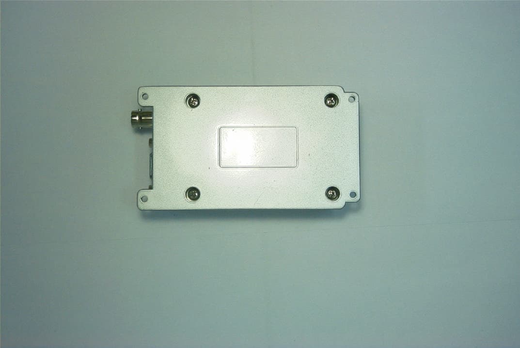
Click to zoom
Application Details
- Equipment Class
- TNB - Licensed Non-Broadcast Station Transmitter
- Date of Grant
- Jun 12, 2003
- Application Purpose
- Original Equipment
- Date of Application
- Jun 12, 2003
- Equipment Note
- VHF Radio Transmitter
- Frequency Range
- 148.00000000 - 174.00000000
- Company
- Midland Radio Corporation
- Country
- United States
Documents & Files
Document Text
Text extracted from the exhibit documents filed with the FCC. Open a document above to read the original.
Users Manual
SD-161 / SD-164 Data Radio User Instruction Manual 2 FCC RF Exposure Compliance Requirements The Federal Communications Commission (FCC), with its action in General Docket 93-62, November 7, 1997, has adopted a safety standard for human exposure to Radio Frequency (RF) electromagnetic energy emitted by FCC regulated equipment. Topaz3 / Maxon subscribes to the same safety standard for the use of its products. Proper operation of this radio will result in user exposure far below the Occupational Safety and Health Act (OSHA) and Federal Communications Commission limits. Power listed is conducted. This device must not exceed a maximum transmitting duty factor of 50%. The antenna(s) used for this transmitter must be installed to provide a separation distance of at least 49cm (19 inches) from all persons, must not be co-located or operating in conjunction with any other antenna or transmitter, and must not exceed a gain of 5 dBd for SD-161 and 7 dBd for SD-164. Failure to observe these restrictions will result in exceeding the FCC RF exposure limits. About your SD-160 Series Data Radio The SD-160 Series of RF Link Modules from Topaz3 utilize the latest technology in their designs and manufacturing. SD- 160 models are Phase Lock Loop Synthesizer (PLL) / microprocessor controlled and offer two (2) watts of power with 16- channel capability. Multiple functions including 1200 to 9600 baud rates, AC and/or DC audio coupling, GMSK, FFSK and FSK modulation are standard in these fully programmable RF Link Module units. Programmable sub-audio squelch system (CTCSS & DCS) and two-tone squelch system are added to the signal level detect squelch system (RSSI). GPS Data handling is provided to interface and control an internal GPS receiver. To assure satisfaction from the radio, we urge you to thoroughly read the operation and function information in this manual before operating your SD-161/SD-164. Applications of some of the functions described in this manual are determined by the system you use. Your Topaz3 dealer will program your radio so that you have the greatest number of functions possible relative to your needs. Should you have questions regarding the operation of the radio, please consult your Topaz3 Dealer. 3 Specifications GENERAL Equipment Type ............................................................... Data radio Performance Specifications ................................................TIA / EIA-603 Band .............................................................................. VHF(SD-161) / UHF(SD-164) Channel Spacings ............................................................ 25 kHz, 12.5 kHz programmable RF Output Power ............................................................ 2 watt only Modulation Type ............................................................ F2D, F3E Intermediate Frequency ................................................... 45.1 MHz & 455 kHz Number of Channels ......................................................... 16 Frequency Source ............................................................ Synthesizer Operation Rating ............................................................ Intermittent 90 : 5 : 5 (Standby: RX: TX) Power Supply .................................................................. Ext. Power Supply(12 VDC Nominal) 7.2V - 18.0V DC EXTREME Temperature Range Storage ........................................................................... from - 40°C to + 80°C Operating ........................................................................ from - 30°C to + 60°C Current Consumption Standby (Muted) ............................................................... < 65 mA Transmit 2 Watt RF power ................................................ < 1.0 A Frequency Bands: RX TX VHF : V2 148.000 - 174.000 MHz 148.000 - 174.000 MHz UHF : U2 450.000 - 490.000 MHz 450.000 - 490.000 MHz Lock Time ........................................................................ < 10 mS TX to RX attack time ......................................................... < 20 mS (No Power Saving) RX to TX attack time ......................................................... < 20 mS Dimensions..................................................................... (32 mm)H x (58 mm)W x (125 mm)D Weight ........................................................................... 253 grams 4 TRANSMITTER Specification Carrier Power: .................................................................. Nom. Max. Min. 2W < 3W > 1.5W Sustained Transmission ................................................... Nominal conditions Time : 5 10 30 Sec. Power: >90% >85% >80% Frequency Error ............................................................... < 0.75 kHz Nominal condition for UHF ±5.0 ppm Extreme condition for UHF Frequency Deviation: 25 kHz Channel Spacing ................................................... Peak ±5.0, Min. ±3.8 12.5 kHz Channel Spacing................................................ Peak ±2.5, Min. ±1.9 Audio Frequency Response................................................ Within +1/-3dB of 6dB octave @ 300 Hz to 2.55 kHz for 12.5 kHz C.S. @ 300 Hz to 3.0 kHz for 25 kHz C.S. Adjacent Channel Power 25 kHz ........................................................................... < 70 dBc @ Nominal Condition < 65 dBc @ Extreme Condition 12.5 kHz ........................................................................ < 60 dBc @ Nominal Condition < 55 dBc @ Extreme Condition Conducted Spurious Emission .......................................... < -60 dBc Modulation Sensitivity ...................................................... 100mV RMS @ 60 % Peak Dev. Hum & Noise: 25 kHz Channel Spacing ................................................... > 40 dB (with no PSOPH) 12.5 kHz Channel Spacing ................................................ > 40 dB (with PSOPH) Modulation Symmetry ...................................................... < 10 % Peak Dev @ …
Text truncated - open the document above for the full version.
Internal Photos
Page 1 of 1 6/6/03file://T:\T\Topaz3LLC_O7J\566UT3\566UT3_Int1.JPG Page 1 of 1 6/6/03file://T:\T\Topaz3LLC_O7J\566UT3\566UT3_Int2.JPG Page 1 of 1 6/6/03file://T:\T\Topaz3LLC_O7J\566UT3\566UT3_Int3.JPG Page 1 of 1 6/6/03file://T:\T\Topaz3LLC_O7J\566UT3\566UT3_Int4.JPG Page 1 of 1 6/6/03file://T:\T\Topaz3LLC_O7J\566UT3\566UT3_Int5.JPG Page 1 of 1 6/6/03file://T:\T\Topaz3LLC_O7J\566UT3\566UT3_Int6.JPG Page 1 of 1 6/6/03file://T:\T\Topaz3LLC_O7J\566UT3\566UT3_Int7.JPG Page 1 of 1 6/6/03file://T:\T\Topaz3LLC_O7J\566UT3\566UT3_Int8.JPG Page 1 of 1 6/6/03file://T:\T\Topaz3LLC_O7J\566UT3\566UT3_Int9.JPG Page 1 of 1 6/6/03file://T:\T\Topaz3LLC_O7J\566UT3\566UT3_Int10.JPG
Operational Description
1 BRIEF CIRCUIT DESCRIPTION INTRODUCTION The VHF and UHF radio comprise two PCBs (RF and digital PCB). These boards are connected by 18- pin female and male connector. The digital board which controls radio and data receiving and sending is interfaced with external data equipment through the 15-pin d-sub female (DB-15) connector. DIGITAL CIRCUITS The Digital circuit contains the CPU, the channel select switch, and associated digital circuits. TX-SIGNAL CIRCUIT Generally, there are two signal paths in the TX-signal circuit. One is FSK data signal path and the other is audio signal path. In case of FSK data signal from Pin 1 of DB-15 connector (CON401) goes through IC406-C. That is amplified by IC404-C and then its amplitude is limited by IC404-D. After that, this signal is filtered by 8th order low pass filter (IC405) in order to reduce the required transmission bandwidth. First one stages of 8th order LPF consist of Gaussian filter for the improvement of ramp function response and last three stages use Butterworth filter to have enough attenuation. The output of LPF is then fed to the RF board for TX modulation. Audio signal from Pin 7 of DB-15 connector is fed into the 300Hz High pass filter (IC408) through the IC406-B and IC409. HPF removes sub-audible voice products for application of Sub-audio (Tone) squelch system (CTCSS, DCS) and then the output from IC408 is fed into IC404-A&B with associated parts forming a mic amplifier and pre-emphasis circuit. After that, the pre-emphasized TX-audio signal is inputted to the RF board for TX modulation through FSK data signal path. RX-SIGNAL CIRCUIT The RX signal circuit also has two signal paths. One is data signal path and the other is audio signal path. The RX signal comes from the pin 10 of CON405 of Digital board connected with pin 10 of CON1 in RF board. In case of data signal, switched in IC406-D by Busy signal which is activated when radio receives valid RF signal, it is filtered by IC416-A and then its amplitude level is adjusted (amplified) by IC416-B. The amplitude-adjusted signal goes to pin 2 of DB-15 connector (CON401). In the meantime, audio signal is inputted to the 300Hz High pass filter (IC408) to eliminate sub-audible voice products via IC409. The output of HPF is switched by IC406-A and de-emphasized by resister R471 and C452. After that, its level is adjusted by RV401 and then amplified by IC412 (LM386: Audio 2 amplifier). The amplified signal flows into pin 9 of CON401 (DB-15). ANALOG SWITCH IC409 (MC14053B) is a digitally controlled analog switch which internally consists of three single poles and double throw switches. Besides, there are three control lines, A, B, and C set a high at 5V or low at 0V respectively. The A controls the X ports, the B controls the Y ports, and the C controls the Z ports. Example: A high on control A would connect X to X1.Alow on control A would connect X to X0. HIGH PASS FILTER The 300Hz high pass filter is an 8-pole 1dB Chebeyshev active filter that comprises IC410 and peripheral components. Received audio passes to IC408 from Pin 4 of IC409 where sub-audible tones below 300Hz are removed. TX (Mic)audio is also fed into IC408 via IC409 (Pin 4) where sub-audible voice products below 300Hz are also removed. CTCSS/DCS DECODE CIRCUITS Discriminated audio from Pin 9 of IC6 is fed into IC411-B and associated parts which are the first 2 poles part of a 6th order 250 Hz Chebeyshev low pass filter. The output from pin 1 (IC411-B) is fed into IC409 (Pin 2) and out at pin 15 (IC409). The output signal is then fed to Pin 8 on IC410 which is a 6th order low pass Butterworth switched capacitor filter. The output from the Butterworth filter (Pin 3 of IC410) is then fed to the remaining second 4 poles part of the 6th order Chebeyshev filter, which consist of IC411-D and one of the two internal operational amplifiers of IC410 (MSNBLPS) along with associated components. Both the Chebeyshev and the Butterworth filter are combined to make a 4dB ripple low pass filter when programmed for 250Hz. The output of IC411-D (Pin 14) is fed into the remaining internal operational amplifier of IC410 (MSNBLPS) which forms the squaring circuit for the signal decode. The signal is out from Pin 2 of IC411 (MSNBLPS) and fed into IC401 (MCU) where it is compared whether that is matched with a preprogrammed data or not. If matched, a valid data is decoded and shown by a green L.E.D. on the top panel of the SD-160 data radio, and audio is released through pin 9 of DB-15 Connector. If unmatched, the busy Yellow L.E.D. would be shown. CTCSS/DCS ENCODE CIRCUITS During TX encode, the tone squelch digital signal is produced as a 3-bit parallel word at Pins 33, 34, and 35 of the micro controller (IC401). The 3-bit digital signal is converted to an analog signal by resistors 3 R481, 482 and 483. The analog signal is fed into Pin 1of IC409 and out on Pin 15 (IC409) and again flowed into Pin 8 of IC410 (6th order Butterworth clock tuned low pass filter). The filtered encode output from Pin 3 (IC410) is fed to IC411-A and RV402 (sub-audible gain control), the output at IC411-A is then fed to the audio mixer circuit of RF board. TWO TONE DECODE CIRCUITS Two tone uses same frequency with audio. Discriminated audio from the RF board is inputted to the comparator (two tone decoder: IC403-B) which forms the squaring circuit for the decode signal. The signal is out from Pin 7 of IC403-B and fed into IC401 (MCU) where it is compared whether that is matched with a preprogrammed data or not. If matched, a valid data is decoded, which is shown by a green L.E.D. on the top panel of the SD-160 data radio and audio is released through pin 9 of DB-15 Connector. If unmatched, the busy Yellow L.E.D. would be shown. RSSI DETECTOR From the RF board, the RSSI (Received Signal Strength Indicator) signal flows to Pin 31 of IC401(MCU) through R513. Micro controller unit (IC401) detects received signal level using the inner 8-bit ADC(Analog to Digital Converter)…
Text truncated - open the document above for the full version.
Parts List/Tune Up Info
TUNING PROCEDURE The SD-160 series UHF/VHF Transceiver have broad band covering range, UHF(400-440 MHz & 450- 490 MHz) and VHF(148-174 MHz) and should require no special alignment, unless repairs are performed on the transceiver portion. Should repairs be necessary, use the "Test Equipment Diagram" and the Alignment Points Diagram", in conjunction with the following procedures: • An Extender Board(ACC-516) is required in order to separate the Digital and RF PCB’s to allow access to the alignment points. Installation instructions are provided with the Extender Board Assembly. RECEIVER RX VCO RX VCO is pre-tuned at factory and no more adjustment is required. To identify existence of defect of RX VCO, check the VCO Control voltage. 1. Set the unit to the highest receive frequency, 490MHz(UHF2), 174MHz(VHF) and check the VCO control voltage is under 10.0 Volts. If it’s over 10.0 Volts, adjust C308 of RX VCO to 10.0 Volts 2. Set the unit to the lowest receive frequency 450MHz(UHF2), 148MHz(VHF) and check that the VCO voltage is above 1.5 Volts. Adjust C308 to 1.5 Volts • Note: Use TP1 to measure the voltage. AUDIO OUTPUT LEVEL Adjustment 1. Select a receiver channel that is programmed for Standard band (25kHz) operation. 2. Prepare standard test signal as follows. Set the RF signal generator to the receiver frequency. And then set the AF modulation signal to 1 kHz at 3kH deviation. Adjust the RF output level of the RF signal generator to –47dBm. 3. Apply a standard test signal to the receiver antenna terminals. 4. Adjust RV401 for the specific audio output level. LEVEL SHIFTER for Modem option Board (ACC-513, ACC-514) 1. Select a receiver channel which is programmed for Standard band (25kHz) operation. 2. After Preparing standard test signal for Standard band, apply that signal to the antenna terminals of receiver. 3. Adjust RV403 until the center voltage of demodulated signal (1KHz sine wave) of TP401 is 2.5 Volts. 4. Select a receiver channel which is programmed for Narrow band (12.5kHz) operation. 5. After Preparing standard test signal for Narrow band (only decrease deviation of AF modulation signal as 1.5K from standard test signal for Standard band), apply that signal to the antenna terminals of receiver. 6. Check the center voltage of demodulated signal of TP401 is 2.5 Volts. If different, Adjust RV403 until the center voltage is near 2.5 Volts for each band (25KHz / 12.5KHz). TRANSMITTER Connect the unit to a Service Monitor with the power meter set to the 10W scale (or Autorange) TCXO Set the channel selector to the mid-range frequency 470 MHz, adjust TCXO1 for a reading of 470MHz ±200Hz (155 MHz VHF models). TX VCO TX VCO is pre-tuned at factory and no more adjustment is required. To identify existence of defect of TX VCO, check the VCO Control voltage. 1. Set the unit to the highest transmit frequency, 490MHz(UHF2), 174MHz(VHF) key the transmitter and check the VCO control voltage is under 10.0 Volts. If it’s over 10.0 Volts, adjust C208 of TX VCO to 10.0 Volts. 2. Set the unit to the lowest transmit frequency 450MHz(UHF2), 148(VHF) key the transmitter and check that the VCO voltage is above 1.5 Volts. Adjust C208 to 1.5Volts • Note: use TP1 to measure the voltage. CTCSS, DCS & TX Deviation and Balance Adjustment 1a. Set the unit to a mid-frequency range and a CTCSS of 67Hz. Push PTT and adjust RV402 for desired CTCSS tone deviation. 1b. Switch to a channel with the same frequency and CTCSS of 250.3Hz. Push PTT and adjust RV1 to desired CTCSS tone deviation, same as above step. 1c. Switch between the 67Hz channel and the 250.3Hz channel and adjust RV1 until the deviation is the same on both channels. It may be necessary to readjust RV402 to get the desired deviation. 2. Set the unit to a mid-frequency and input the TX data with 400 Hz standard audio level. 3. Increase the signal level to 20 dB from standard level. 4. Monitor the demodulated signal from service monitor. Adjust RV1 to make the monitored signal to be a balanced square wave. 5. Reduce input signal to the standard level and adjust RV2 for the standard deviation. APC 1. Adjust RV4 for High Power (2W, SD-161 & SD-164), (5W, SD-160) 2. Adjust RV3 for Low Power (1W) (SD-160 only) 3. This completes the transmitter alignment procedures. SQUELCH ADJUSTMENT Before squelch adjustment, user should select SQ type. With new SD-160 series, squelch level to open or close (un-mute or mute) is set up by not only software control but also hardware control. It’s programmed by system option of ACC-916. SQUELCH Adjustment (Noise SQ only) 1. Select a receiver channel which is programmed for narrow band (12.5kHz) operation. 2. Set the RF signal generator to the receiver frequency. Set the AF modulation signal to 1 kHz at 1.5kH deviation. 3. Adjust the RF output level of the RF signal generator until the 1kHz signal is heard. 4. Adjust the RF signal to the desired level for squelch sensitivity as you monitor SINAD. This is usually 8 to 12 dB SINAD. 5. On the RF board, adjust RV5 until the squelch is justly un-muted (open). 6. Switch off the RF generator (squelch should be closed). 7. Switch on the RF generator, Squelch should be opened at the SINAD point where RV5 was adjusted. 8. Select a receiver channel that is programmed for wide band operation (25kHz). 9. Set the RF signal generator to the receiver frequency. Set the AF modulation signal to 1 kHz at 3kH deviation. 10. Adjust the RF output level of the RF signal generator until the 1kHz signal is heard. 11. Adjust the RF signal to the desired level for squelch sensitivity as you monitor SINAD. This is usually 8 to 12 dB SINAD. 12. On the RF board, adjust RV6 until the squelch is justly un-muted (open). 13. Switch off the RF generator (squelch should be closed). 14. Switch on the RF generator, Squelch should be opened at the SINAD point where RV6 was adjusted. 15. Disconnect the test equipment. SQUELCH Adjustment (RSSI SQ only) using ACC-2016 & ACC-916 Default setting of squelch level for …
Text truncated - open the document above for the full version.
Test Report
APPLICANT: TOPAZ3, LLC FCC ID: O7KSD161 REPORT #: T/Topaz3LLC_O7J\566UT3\566UT3TestReport.doc TABLE OF CONTENTS TABLE OF CONTENTS LIST FOR PART 90 VHF DEVICE APPLICANT: TOPAZ3, LLC FCC ID: O7KSD161 TEST REPORT: PAGE 1...........GENERAL INFORMATION & TECHNICAL DESCRIPTION PAGE 2...........TECHNICAL DESCRIPTION CONTINUED & RF POWER OUTPUT PAGE 3-5.........VOICE MODULATION CHARACTERISTICS PAGE 6...........AUDIO LOW PASS FILTER AND AUDIO FREQUENCY RESPONSE PAGE 7-8.........OCCUPIED BANDWIDTH PAGE 9-13........OCCUPIED BANDWIDTH PLOTS PAGE 14-15.......SPURIOUS EMISSIONS AT ANTENNA TERMINALS PAGE 15..........METHOD OF MEASURING SPURIOUS EMISSIONS AT ANTENNA TERM. PAGE 16..........FIELD STRENGTH OF SPURIOUS EMISSIONS PAGE 17..........METHOD OF MEASURING RADIATED SPURIOUS EMISSIONS PAGE 18..........FREQUENCY STABILITY PAGE 19-20.......TRANSIENT FREQUENCY STABILITY PAGE 21-22.......TRANSIENT FREQUENCY RESPONSE PLOTS PAGE 23..........MPE CALCULATION PAGE 24-27.......LIST OF TEST EQUIPMENT EXHIBITS CONTAINING: EXHIBIT 1.........FCC ID LABEL SAMPLE & LOCATION EXHIBIT 2.........SCHEMATIC EXHIBIT 3.........BLOCK DIAGRAM EXHIBIT 4.........USERS MANUAL EXHIBIT 5.........OPERATIONAL DESCRIPTION EXHIBIT 6.........EXTERNAL PHOTOGRAPHS EXHIBIT 7.........INTERNAL PHOTOGRAPHS EXHIBIT 8.........TUNING PROCEDURE EXHIBIT 9.........PARTS LIST EXHIBIT 10........TEST SET UP PHOTOGRAPH APPLICANT: TOPAZ3, LLC FCC ID: O7KSD161 REPORT #: T/Topaz3LLC_O7J\566UT3\566UT3TestReport.doc Page 1 of 27 GENERAL INFORMATION REQUIRED FOR TYPE ACCEPTANCE 2.1033 TOPAZ3, LLC will sell the (c)(1)(2) FCC ID: O7KSD161 VHF transceiver in quantity, for use under FCC RULES PART 90. 2.1033 (c) TECHNICAL DESCRIPTION 2.1033 (3) User Manual See Exhibit 4 2.1033 (4) Type of Emission: 11K25F2D F2D emission: ALLOWED AUTHORIZED BANDWIDTH = 11.25 kHz. Bn = 2M + 2DK M = 9600 Bits per second D = 825 Hz (Peak Deviation) K = 1 Bn = 2(9600/2) + 2(825)(1) = 9.6k + 1.65k = 11.25k Type of Emission: 11K0F3E F3E emission and 12.5 kHz channel spacing: ALLOWED AUTHORIZED BANDWIDTH = 11.25 kHz. Bn = 2M + 2DK M = 3 kHz D = 2.5kHz (Peak Deviation) K = 1 Bn = 2(3) + 2(2.5)(1) = 11k Type of Emission: 14K7F3E F3E emission and 25 kHz channel spacing: ALLOWED AUTHORIZED BANDWIDTH = 20 kHz. Bn = 2M + 2DK M = 3 kHz D = 4.35 kHz (Peak Deviation) K = 1 Bn = 2(3) + 2(4.35)(1) = 14.7k 90.209(b)(5) 2.1033 (5) Frequency Range: 148-174 MHz (6) Power Range and Controls: There are NO user Power controls. (7) Maximum Output Power Rating: See Next Page. (8) DC Voltages and Current into Final Amplifier: Maximum POWER INPUT for 2 Watt rated output power FINAL AMPLIFIER ONLY Vce = 12.0 Volts IC = .42 A P = 5.04 Watt APPLICANT: TOPAZ3, LLC FCC ID: O7KSD161 REPORT #: T/Topaz3LLC_O7J\566UT3\566UT3TestReport.doc Page 2 of 27 (9) Tune-up procedure. The tune-up procedure is given in EXHIBIT 8. 2.1033 (10) Complete Circuit Diagrams: The circuit diagram is included as EXHIBIT 2. The block diagram is included as EXHIBIT 3. (11) Function of each electron tube or semiconductor device or other active circuit device: -SEE EXHIBIT 9. (8) Instruction book. The instruction manual is included as EXHIBIT 4. (10) Description of all circuitry and devices provided for determining and stabilizing frequency is included in the circuit description in EXHIBIT 5. 2.1033(c)(11) A photograph or drawing of the equipment identification label is shown in EXHIBIT 1. 2.1033(c)(12) Photographs of the equipment of sufficient clarity to reveal equipment construction and layout and label location are shown in Exhibit 6-7. 2.1033(c)(13) For equipment employing digital modulation, a detail description of the modulation technique. This UUT uses FSK to modulate the transmitter. 2.1033(c)(14) data required for 2.1046 to 2.1057 See Below 2.1046(a) RF power output . RF power is measured by connecting a 50 ohm, re- sistive wattmeter to the RF output connector. With a nominal battery voltage of 12.0 VDC, and the transmitter properly adjusted the RF output measures: POWER OUTPUT HIGH – 2 Watts METHOD OF MEASURING RF POWER OUTPUT Transmitter 50 ohm under test Resistive Wattmeter Power Supply APPLICANT: TOPAZ3, LLC FCC ID: O7KSD161 REPORT #: T/Topaz3LLC_O7J\566UT3\566UT3TestReport.doc Page 3 of 27 2.1047(a) Voice Modulation characteristics: MODULATION LIMITING PLOT – 300 Hz – NARROW BAND Modulation Limiting 300Hz 0 500 1000 1500 2000 2500 3000 -90-80-70-60-50-40-30-20-10010 dBm deviation MODULATION LIMITING PLOT – 300 Hz – WIDE BAND Modulation Limiting 300 Hz 0 500 1000 1500 2000 2500 3000 3500 4000 4500 dBm dBm deviation deviation APPLICANT: TOPAZ3, LLC FCC ID: O7KSD161 REPORT #: T/Topaz3LLC_O7J\566UT3\566UT3TestReport.doc Page 4 of 27 MODULATION LIMITING PLOT – 1000 Hz – NARROW BAND Modulation Limiting 1kHz 0 500 1000 1500 2000 2500 3000 -90 -80 -70 -60 -50 -40 -30 -20 -10010 dBm deviatio n MODULATION LIMITING PLOT – 1000 Hz – WIDE BAND Modulation Limiting 1000 Hz 0 500 1000 1500 2000 2500 3000 3500 4000 4500 dBm dBm deviation deviation APPLICANT: TOPAZ3, LLC FCC ID: O7KSD161 REPORT #: T/Topaz3LLC_O7J\566UT3\566UT3TestReport.doc Page 5 of 27 MODULATION LIMITING PLOT – 2.5 kHz – NARROW BAND Modulation Limiting 2.5 kHz 0 500 1000 1500 2000 2500 3000 -90-80-70-60-50-40-30-20-10010 dBm deviation MODULATION LIMITING PLOT – 2.5 k – WIDE BAND Modulation Limiting 2500 Hz 0 500 1000 1500 2000 2500 3000 3500 4000 4500 dBm dBm deviation deviation APPLICANT: TOPAZ3, LLC FCC ID: O7KSD161 REPORT #: T/Topaz3LLC_O7J\566UT3\566UT3TestReport.doc Page 6 of 27 2.1049 Audio Low Pass Filter Post Limite r Plot -60 -50 -40 -30 -20 -10 0 10 100010000100000 Fr e q . Hz Att. dB Audio Frequency response Audio Frequency Repons e -15 -10 -5 0 5 10 0123 456 Frequency (kHz) Level in dB APPLICANT: TOPAZ3, LLC FCC ID: O7KSD161 REPORT #: T/Topaz3LLC_O7J\566UT3\566UT3TestReport.doc Page 7 of 27 2.1049 Occupied bandwidth: 90.210(c,) For transmitters that are not equipped with an audio low pass filter pursuant to S90.211(b), the power of any emission must be attenuated…
Text truncated - open the document above for the full version.
Contact Information
Applicant
Jeff Brame(Director of Engineering)
Test Firm
Timco Engineering, Inc.S Sanders
Technical Specifications
| # | Rule Parts | Frequency Range | Power Output | Emission | Tolerance |
|---|---|---|---|---|---|
| 3 | 9 | 148 MHz - 174 MHz | 2.4 W | 14K7F3E | 2.5 ppm |
Other Applications from Midland Radio Corporation
O7KSD164
Jun 02, 2003UHF Data Transceiver - Transmitter
Equipment Class
TNB - Licensed Non-Broadcast Station Transmitter
O7KML3245
Jan 27, 2003UHF 32 Channel Mobile Radios
Equipment Class
TNB - Licensed Non-Broadcast Station Transmitter
O7KML3215
Jan 09, 200332 Channel Mobile Radio
Equipment Class
TNB - Licensed Non-Broadcast Station Transmitter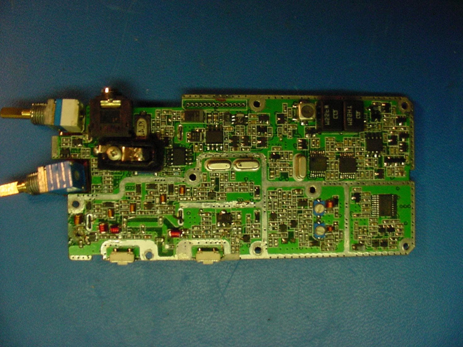
O7KPL5164
May 29, 2002PL5164 Portable Radio
Equipment Class
TNF - Licensed Non-Broadcast Transmitter Held to Face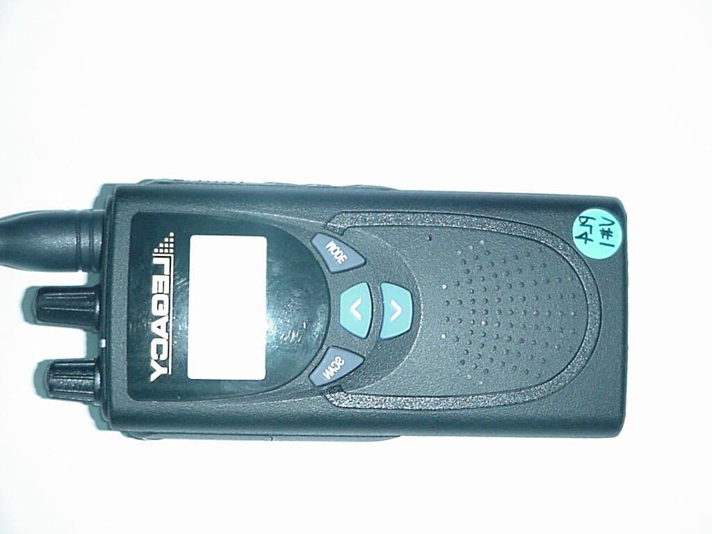
O7KPL5161
Apr 14, 2002PL5161 Portable Radio
Equipment Class
TNF - Licensed Non-Broadcast Transmitter Held to Face