O9TMTX2100Audio/Video Transmitter
M & G Technology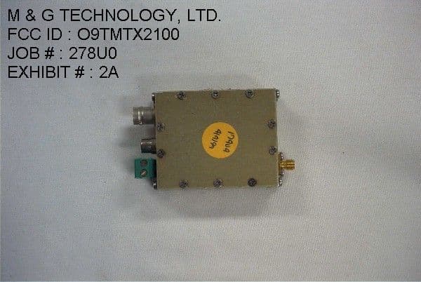
Click to zoom
Application Details
- Equipment Class
- TNB - Licensed Non-Broadcast Station Transmitter
- Date of Grant
- Oct 15, 2000
- Application Purpose
- Original Equipment
- Date of Application
- Oct 15, 2000
- Equipment Note
- Audio/Video Transmitter
- Frequency Range
- 2450.00000000 - 2450.00000000
- Company
- M & G Technology
- Country
- United Kingdom
Documents & Files
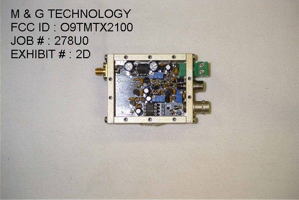
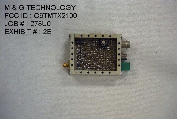
Document Text
Text extracted from the exhibit documents filed with the FCC. Open a document above to read the original.
Test Report
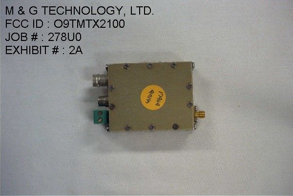
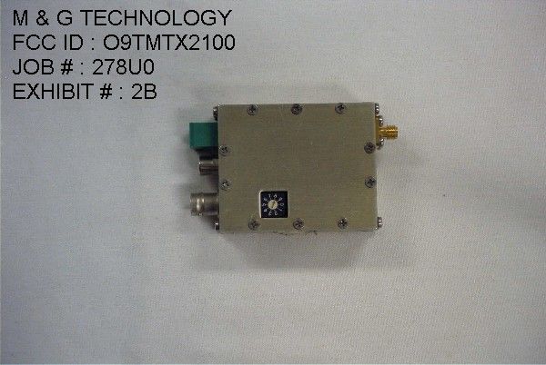
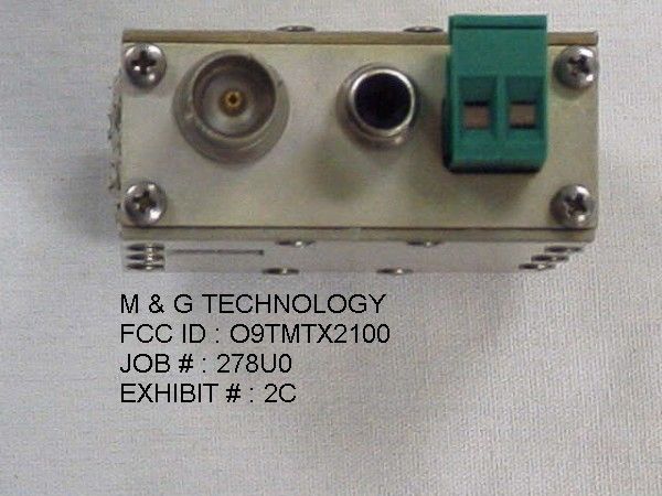
Applicant: M & G Technology, LTD. Report #: T:\cus\M\MGT\278u0-report.doc FCC ID: O9TMTX2100 TABLE OF CONTENTS Date: 3 June 2000 TABLE OF CONTENTS LIST APPLICANT: M&G TECHNOLOGY, LTD. FCC ID: O9TMTX2100 TEST REPORT: PAGE 1......COVER SHEET - GENERAL INFORMATION & TECHNICAL DESCR. PAGE 2......TECHNICAL DESCRIPTION CONTD. & RF POWER OUTPUT AND MODULATION CHARACTERISTICS PAGE 3......OCCUPIED BANDWIDTH PAGE 4......SPURIOUS EMISSIONS AT ANTENNA TERMINALS PAGE 5......FIELD STRENGTH OF SPURIOUS EMISSIONS PAGE 6......METHOD OF MEASURING RADIATED SPURIOUS EMISSIONS PAGE 7......FREQUENCY STABILITY PAGE 8......LIST OF TEST EQUIPMENT EXHIBITS CONTAINING: EXHIBIT 1.........FCC ID LABEL SAMPLE AND SKETCH OF LOCATION EXHIBIT 2A........EXTERNAL FRONT VIEW PHOTOGRAPHS EXHIBIT 2B........EXTERNAL REAR VIEW PHOTOGRAPHS EXHIBIT 2C........EXTERNAL TOP VIEW PHOTOGRAPH EXHIBIT 2D........INTERNAL COMPONENT SIDE PHOTOGRAPH EXHIBIT 2E........INTERNAL SOLDER SIDE PHOTOGRAPH EXHIBIT 3.........BLOCK DIAGRAM EXHIBIT 4.........SCHEMATIC EXHIBIT 5A-5B.....USER'S MANUAL EXHIBIT 6A........OCCUPIED BANDWIDTH PLOT - CW EXHIBIT 6B........OCCUPIED BANDWIDTH PLOT - EXHIBIT 7.........AUDIO FREQUENCY RESPONSE GRAPH Applicant: M & G Technology, LTD. Report #: T:\cus\M\MGT\278u0-report.doc FCC ID: O9TMTX2100 Page Number 1 Date: 3 June 2000 GENERAL INFORMATION REQUIRED FOR TYPE ACCEPTANCE 2.1033(C)(1)(2) M & G TECHNOLOGY, LTD. will sell the FCC ID: O9TMTX2100 transmitter in quantity, for use under FCC RULES PART 90. M & G TECHNOLOGY, LTD. 262 Chamberlayne Road London England NW103LN 2.1033 (C) TECHNICAL DESCRIPTION Type of Emission: 9M5F8F 21033(C)(5) Frequency Range: 2 channels 2425 and 2450 MHz (6) Power Range and Controls: This UUT has a power output of 100 mW (7) 2,1033(c)(b) Maximum Output Power Rating: 100 mWatts into a 50 ohm resistive load. (8) DC Voltages and Current into Final Amplifier: 12 Volts and 0.150 Amperes POWER INPUT FINAL AMPLIFIER ONLY POWER INPUT 1.80 Watts Vce Volts 12 Volts Ice Amps 0.15 Amps 2.1033(c)(9) The tune-up procedure is included in the service manual. 2.1033(c)(10) A schematic in included as in Exhibit 4. Applicant: M & G Technology, LTD. Report #: T:\cus\M\MGT\278u0-report.doc FCC ID: O9TMTX2100 Page Number 2 Date: 3 June 2000 2.1033(c)(11) Photograph or drawing of the label showing the FCC ID and the location of the label – See Exhibit # 1. 2.1033(c)(12) Photographs completely documenting the radio – See Exhibit #’s 2A-2E. 2.1033(c)(13) N/A This is for devices that use digital modulation. 2.1033(c)(14) The data required by 2.1046 through 2.1057 follows; 2.1046(a) RF power output. The test procedure used was TIA/EIA-603 S2.2.1. RF power is measured by connecting a 50 ohm, resistive wattmeter to the RF output connec- tor. With a nominal battery voltage of 12.0V, and the transmitter properly adjusted the RF output measures: INPUT POWER: (12V)(A) = 1.80 Watts OUTPUT POWER: 100 mWatts Efficiency: 5.50% 2.1046(a) RF power output. The test procedure used was TIA/EIA-603 S2.2.1. 2.1047(a) Modulation characteristics: AUDIO FREQUENCY RESPONSE The audio frequency response was measured in accordance with TIA/EIA Specification TIA/EIA-603 S2.2.6.2.1. The audio frequency response curve is shown in Exhibit # 7. 2.1049 AUDIO LOW PASS FILTER Transmitters utilizing analog emissions and meets the requirements of paragraph 90.210(c) therefore no low-pass filter response in included. Applicant: M & G Technology, LTD. Report #: T:\cus\M\MGT\278u0-report.doc FCC ID: O9TMTX2100 Page Number 3 Date: 3 June 2000 2.1049 Occupied bandwidth: 90.210 (c) (1) On any frequency removed from the center of the author- ize bandwidth by a displacement of (fd in kHz) of more than 5kHz but not more than 10kHz At least 83log(fd/5)dB. (2) On any frequency removed from the center of the author- ized bandwidth by a displacement of (fd in kHz) of more than 10kHz but not more than 250%of the authorized bandwidth: At least 29log(fd2/11)dB. (3) On any frequency removed from the center of the author ized bandwidth by a displacement of (fd in kHz) of more than 250% of the authorized bandwidth: At least 43+ 10log(P) dB. See Exhibit 14. 2.1049 Occupied bandwidth: Using TIA/EIA 2.2.11 Spectrum TIA/EIA-603 S2.2.11 was used to measure the occupied bandwidth. Plots were made of the spectrum modulated by an NTSC generator with a full video pattern. Data in the plots show that all sidebands beyond the authorized bandwidth are less than 0.5% of the unmodulated carrier. The plots show the transmitter modulation with; The spectrum analyzer was set with the unmodulated carrier at the top of the screen. The test procedure diagram and occupied bandwidth plots follow. Applicant: M & G Technology, LTD. Report #: T:\cus\M\MGT\278u0-report.doc FCC ID: O9TMTX2100 Page Number 4 Date: 3 June 2000 2.1051 Spurious emissions at antenna terminals(conducted): The following data shows the level of conducted spuri- ous responses at the antenna terminal. The test proce- dure used was TIA/EIA 603 S2.2.13 with the exception that the emissions were recorded in dBc. The spectrum was scanned from 0.4 to at least the 10th harmonic of the fundamental. NAME OF TEST: SPURIOUS EMISSIONS AT ANTENNA TERMINALS REQUIREMENTS: Emissions must be 43 +10log(Po) dB below the mean power output of the transmitter. POWER OUTPUT 43 + 10log(0.1) = 33.0dB Frequency dB below MHz carrier 24250 485050.4 727550.7 970067.1 1212562.7 1455053.7 16975>80 19400>80 21825>80 24250>80 Applicant: M & G Technology, LTD. Report #: T:\cus\M\MGT\278u0-report.doc FCC ID: O9TMTX2100 Page Number 5 Date: 3 June 2000 2.1053 (b) Field strength of spurious emissions: The tabulated Data shows the results of the radiat- ed field strength emissions test. The spectrum was scanned from 30 to the 10 th harmonic. This test was conducted per ANSI C63.4-1992 with the exception of briefly connecting the transmitter to a half wave dipole for the purpose of establishing a reference. NAME OF TEST: RADIATED SPURIOUS EMISSIONS REQUIREMENT…
Text truncated - open the document above for the full version.
Test Report
M & G Technology., LTD. O49MTX2100 4 4.2 4.4 4.6 4.8 5 5.2 5.4 5.6 5.8 6 100100010000100000 Frequency rms mVolts audio response M&G TECHNOLOGY FCC ID: O9TMTX2100 M & G TECHNOLOGY FCC ID : O9TMTX2100 JOB # : 278U0 EXHIBIT # : 7
Contact Information
Applicant
Giovanni Luongo(President)
Test Firm
Timco Engineering, Inc.S Sanders
Technical Specifications
| # | Rule Parts | Frequency Range | Power Output | Emission | Tolerance |
|---|---|---|---|---|---|
| 2 | 9 | 2.45 GHz - 2.45 GHz | 100.00 mW | 9M5F8F | 0.00025 % |